
Shape-Controlled Crystal Growth of Y3Al5O12:Ce Single Crystals with Application of Micro-Pulling-Down Method and Mo Crucibles, and Their Scintillation Properties

 ,
,  ,
,
Abstract
:1. Introduction
2. Materials and Methods
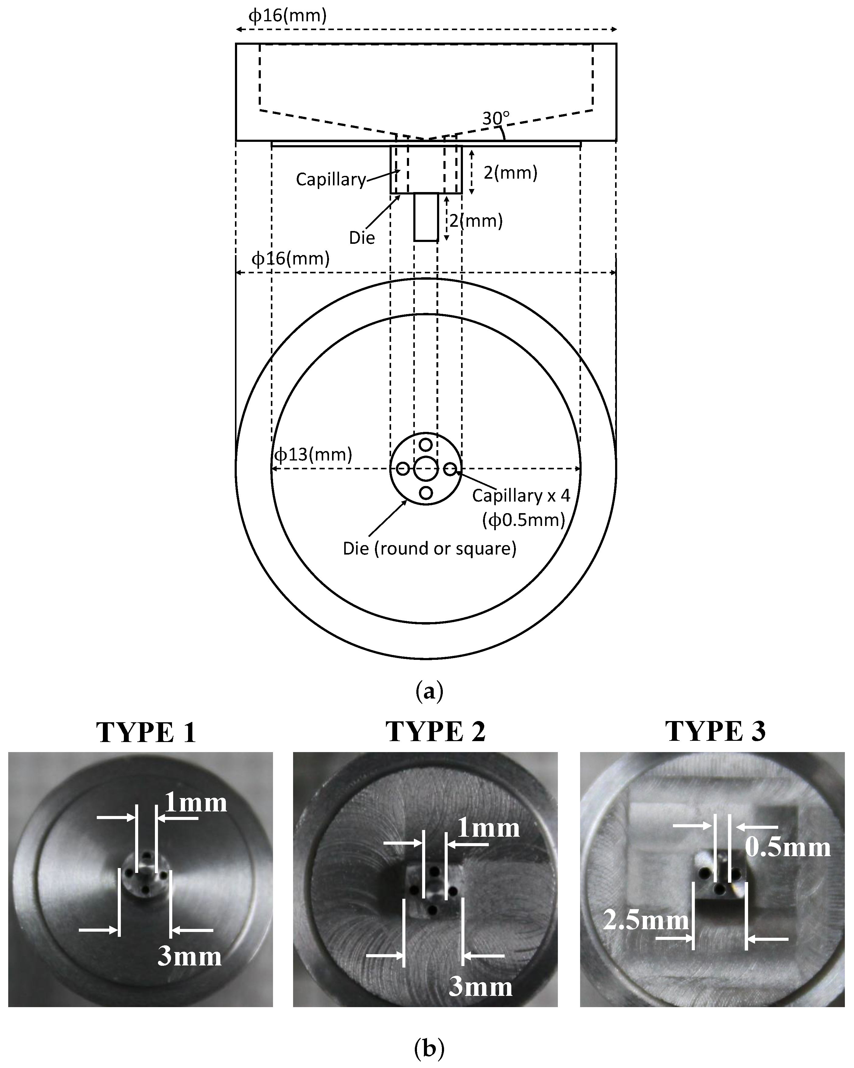
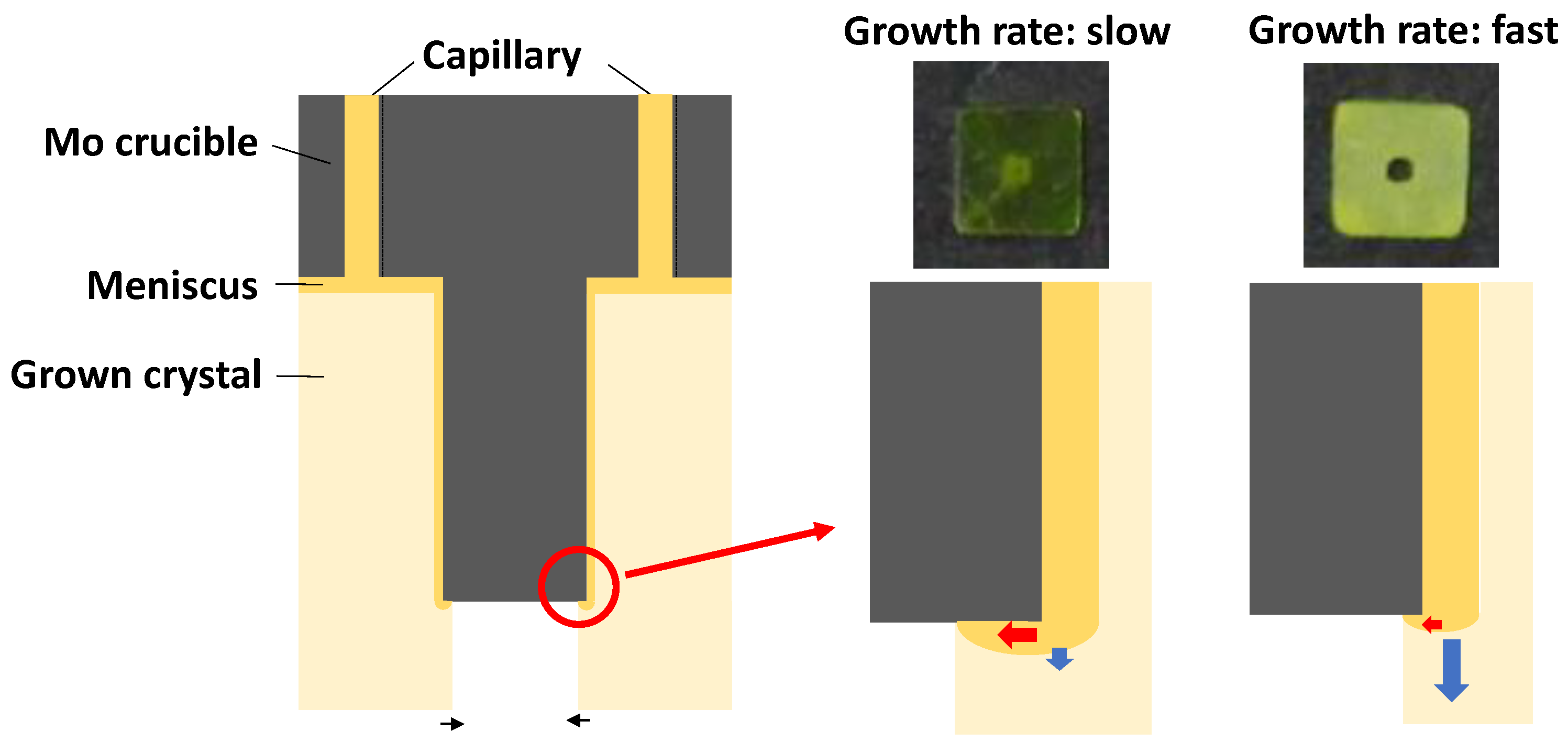
2.1. Mo Crucible with a Tube-Shaped Die
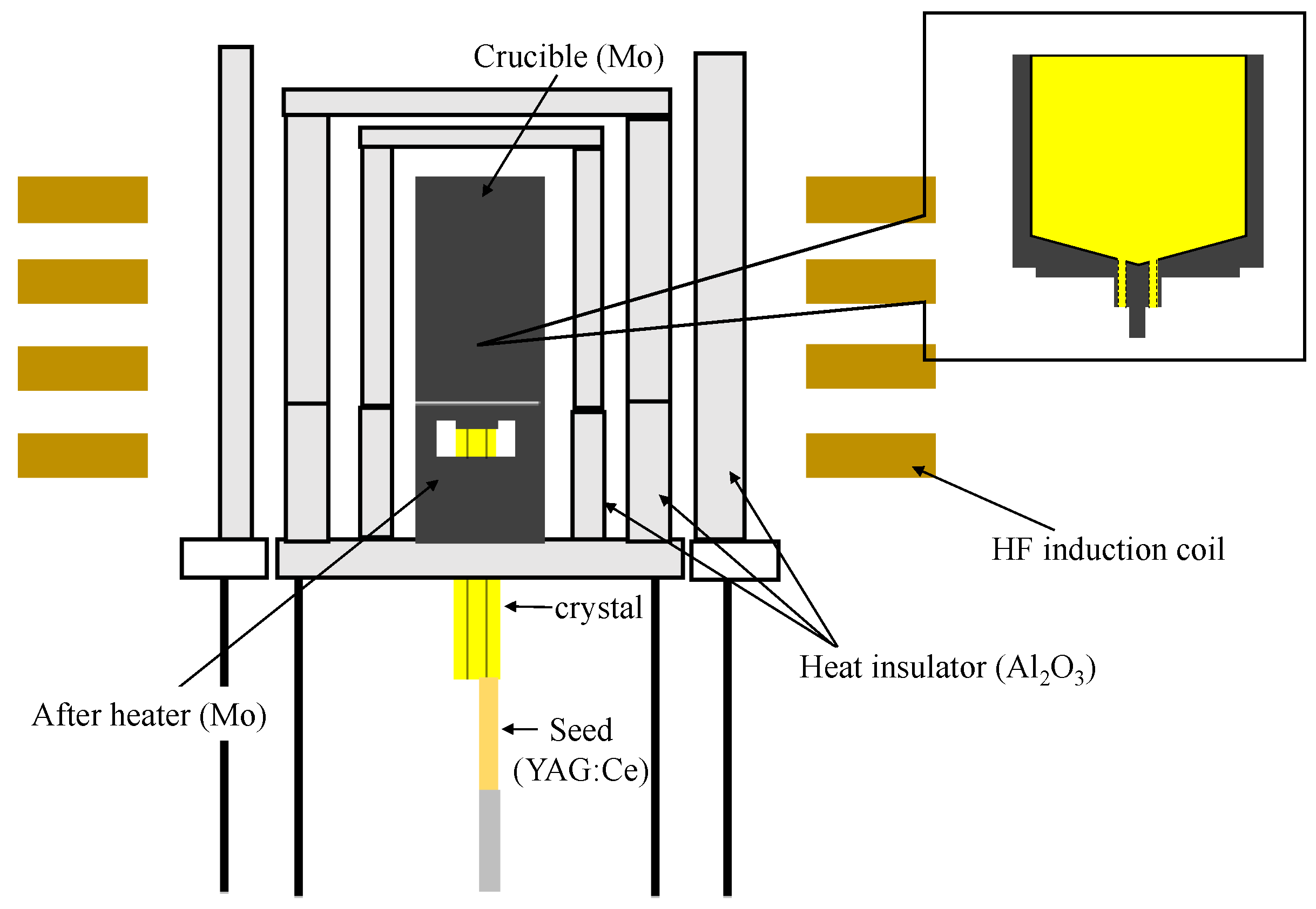
2.2. Crystal Growth Setup
2.3. Characterization
3. Results
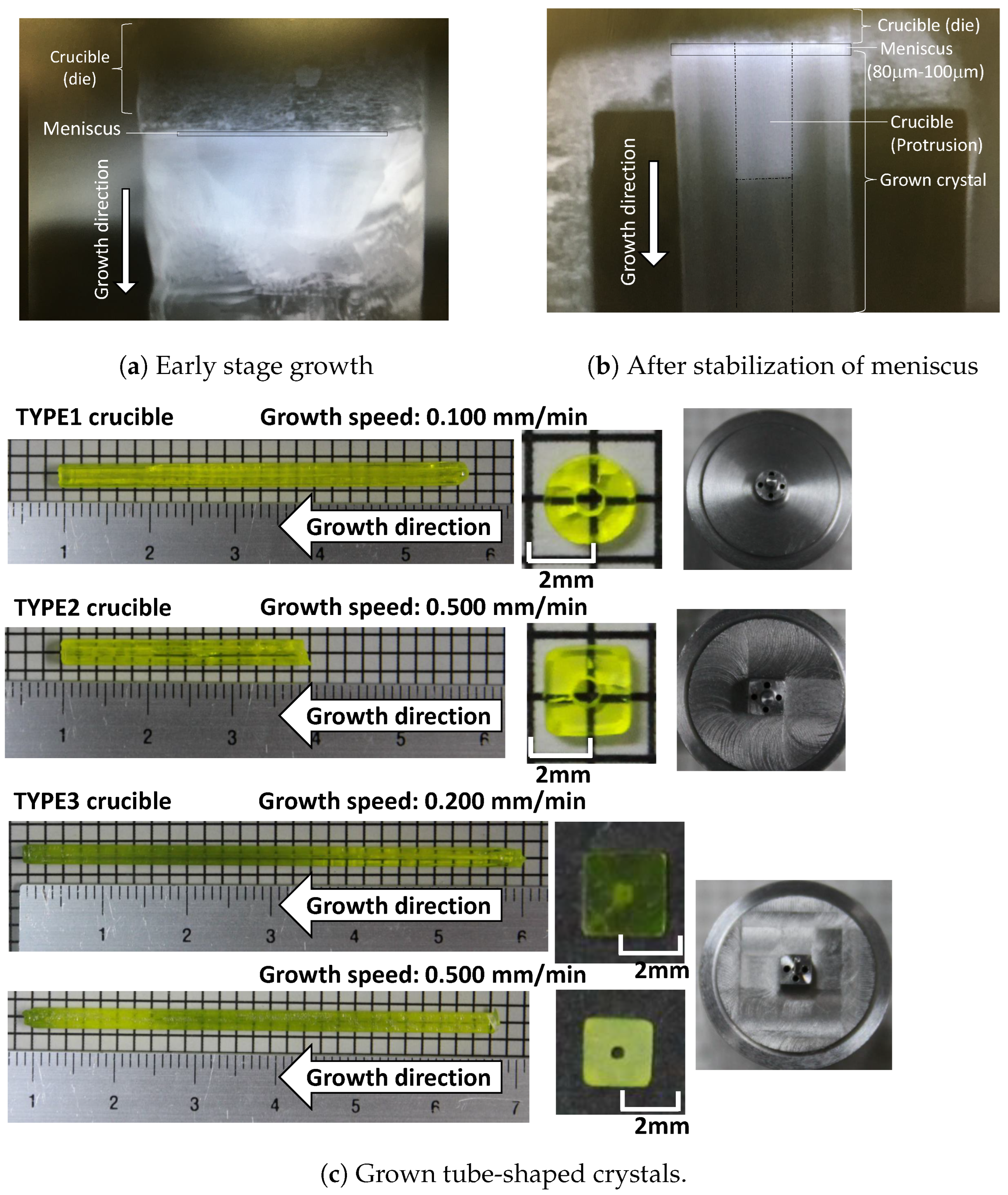
3.1. Crystal Growth
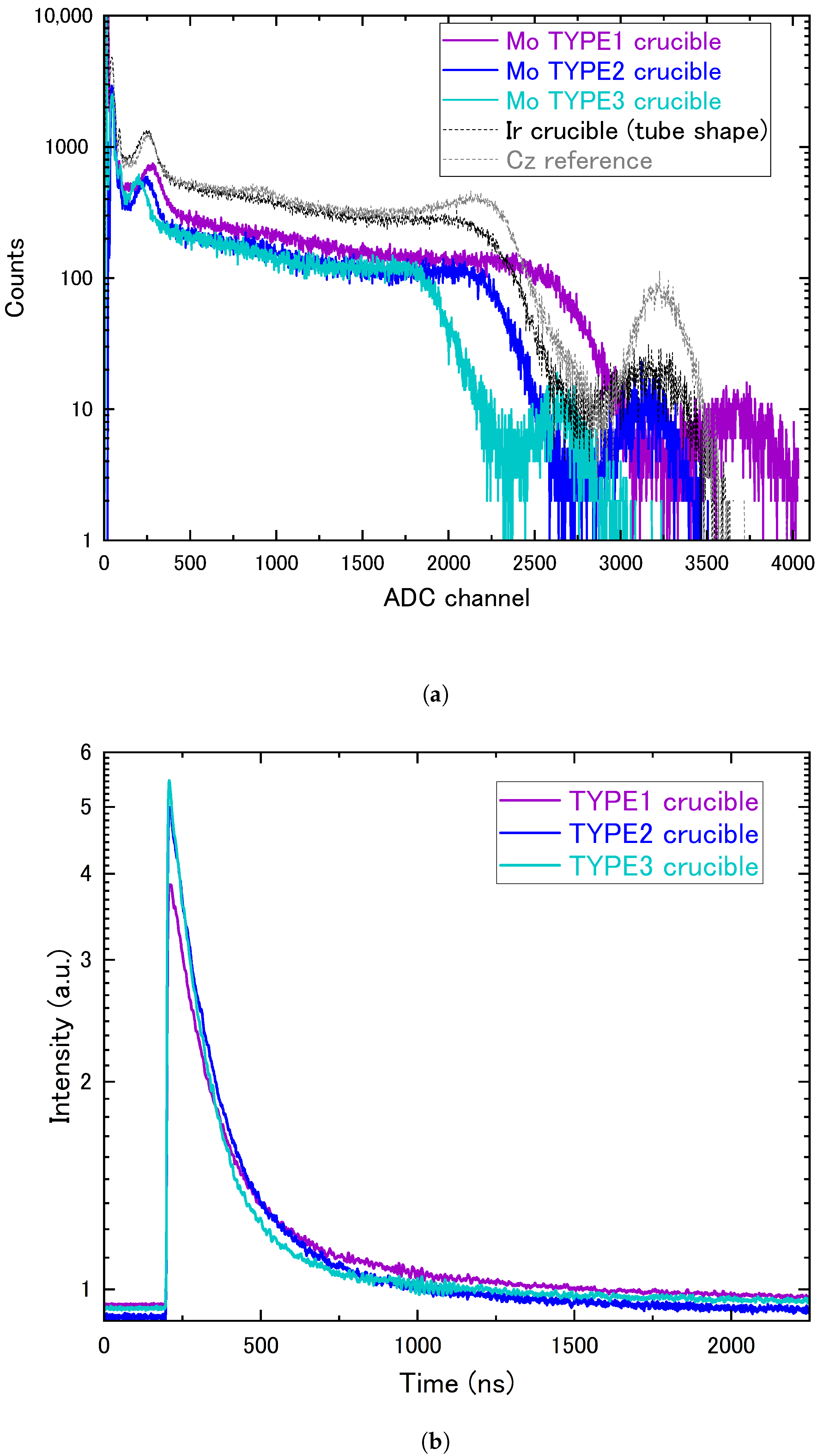
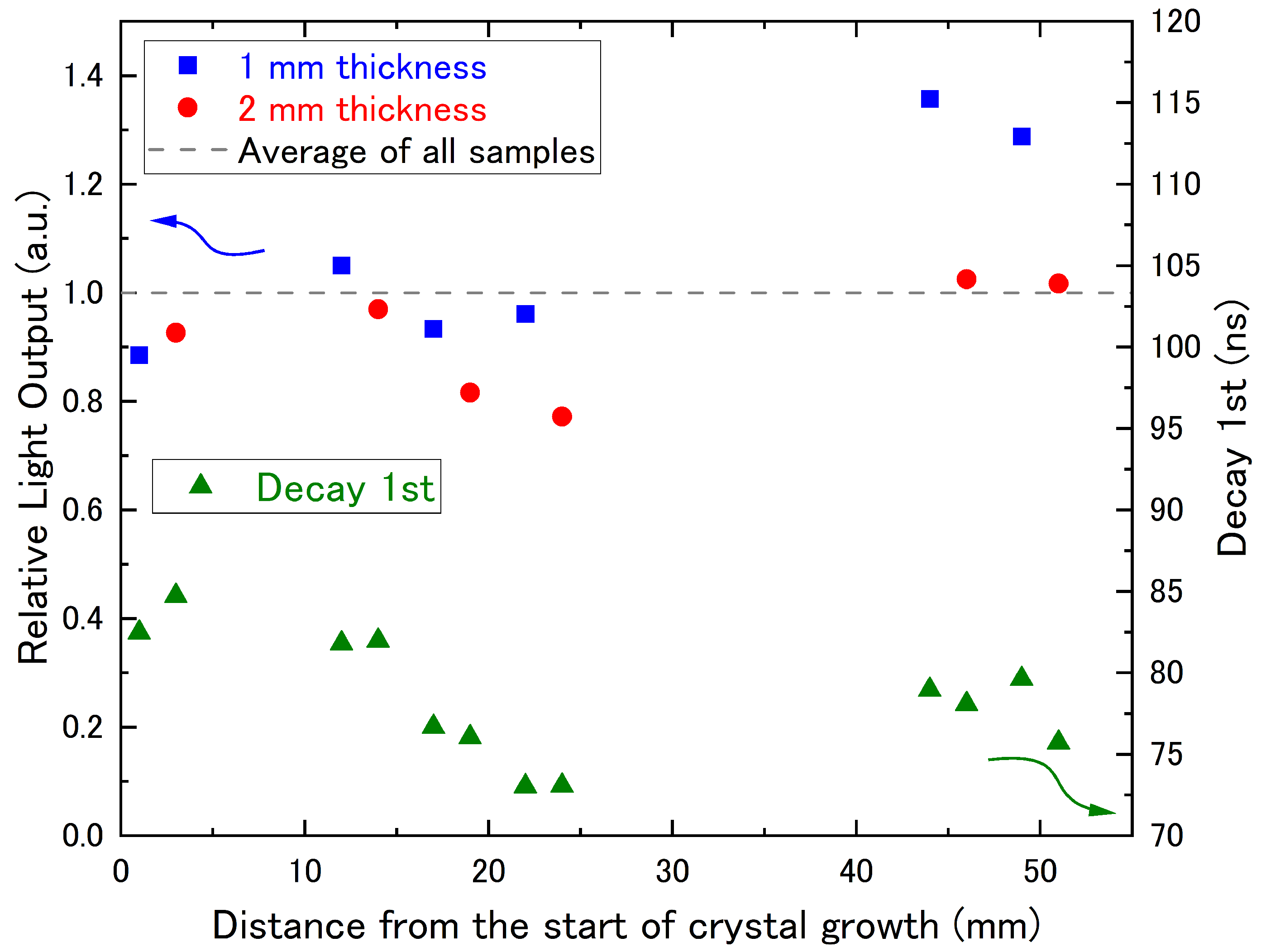
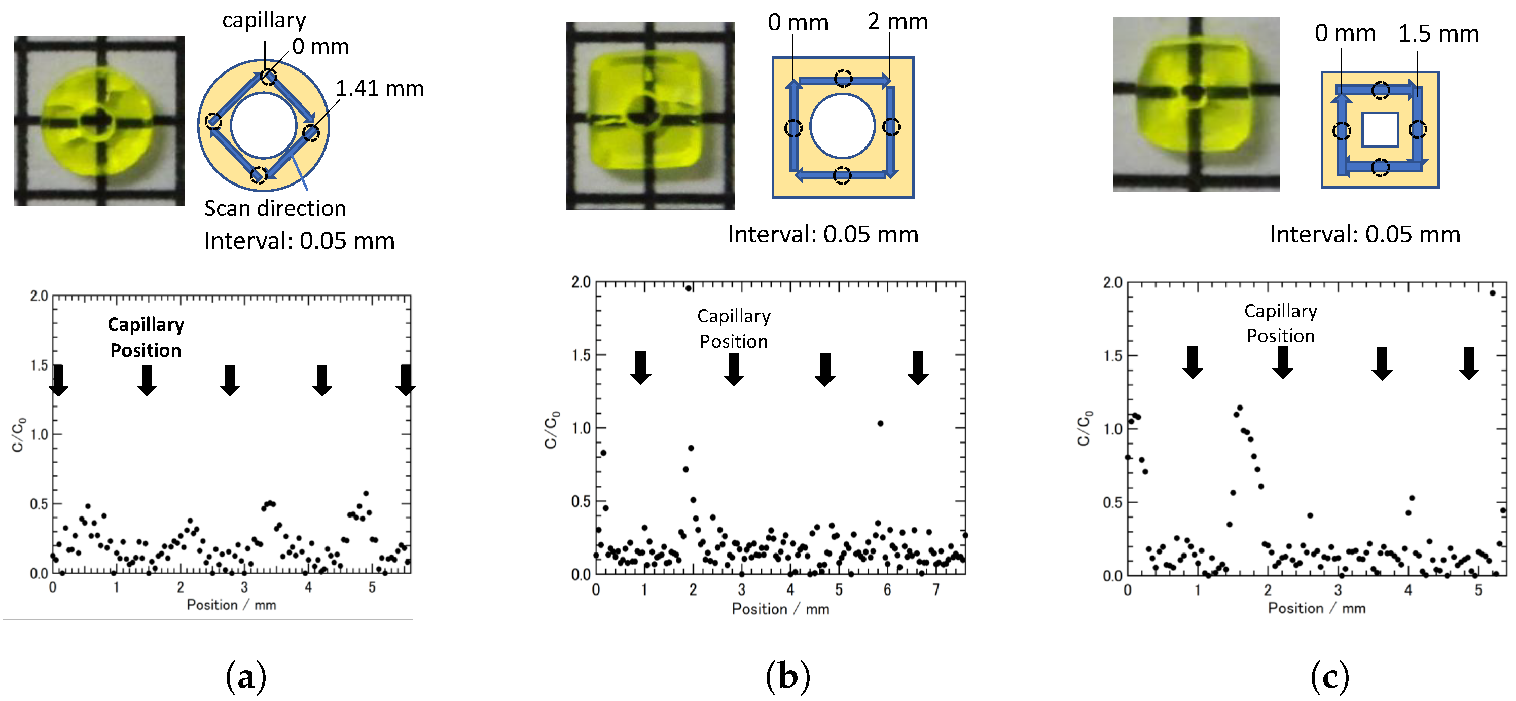
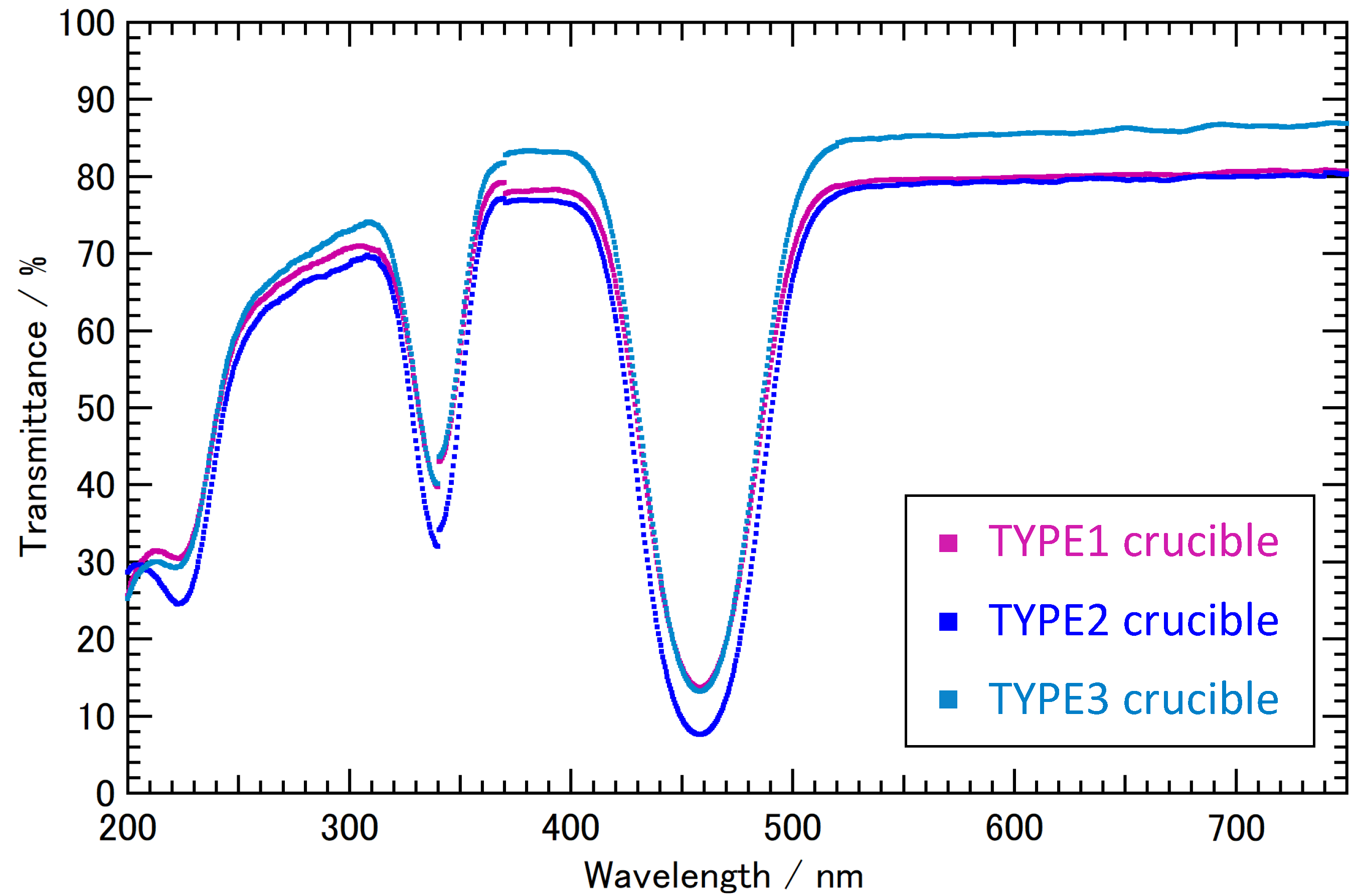
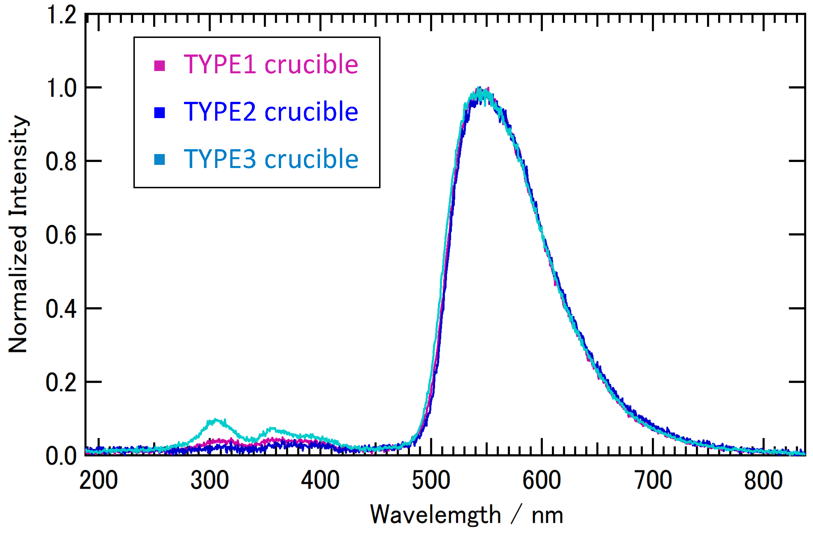
3.2. Optical and Scintillation Properties
4. Conclusions
Author Contributions
Funding
Institutional Review Board Statement
Informed Consent Statement
Data Availability Statement
Acknowledgments
Conflicts of Interest
References
- Nikl, M.; Yoshikawa, A. Recent R&D Trends in Inorganic Single-Crystal Scintillator Materials for Radiation Detection. Adv. Opt. Mater. 2015, 3, 463–481. [Google Scholar] [CrossRef]
- Shimazoe, K.; Yoshino, M.; Ohshima, Y.; Uenomachi, M.; Oogane, K.; Orita, T.; Takahashi, H.; Kamada, K.; Yoshikawa, A.; Takahashi, M. Development of simultaneous PET and Compton imaging using GAGG-SiPM based pixel detectors. Nucl. Instruments Methods Phys. Res. Sect. A Accel. Spectrometers, Detect. Assoc. Equip. 2020, 954, 161499. [Google Scholar] [CrossRef]
- Kodama, S.; Kurosawa, S.; Ohno, M.; Morishita, Y.; Usami, H.; Hayashi, M.; Sasano, M.; Azuma, T.; Tanaka, H.; Kochurikhin, V.; et al. Fiber-read radiation monitoring system using an optical fiber and red-emitting scintillator for ultra-high-dose conditions. Appl. Phys. Express 2020, 13, 047002. [Google Scholar] [CrossRef]
- Lee, T.; Lee, W. A cubic gamma camera with an active collimator. Appl. Radiat. Isot. 2014, 90, 102–108. [Google Scholar] [CrossRef] [PubMed]
- Omata, A.; Kataoka, J.; Fujieda, K.; Sato, S.; Kuriyama, E.; Kato, H.; Toyoshima, A.; Teramoto, T.; Ooe, K.; Liu, Y.; et al. Performance demonstration of a hybrid Compton camera with an active pinhole for wide-band X-ray and gamma-ray imaging. Sci. Rep. 2020, 10, 14064. [Google Scholar] [CrossRef] [PubMed]
- Kamada, K.; Yanagida, T.; Endo, T.; Tsutumi, K.; Usuki, Y.; Nikl, M.; Fujimoto, Y.; Fukabori, A.; Yoshikawa, A. 2inch diameter single crystal growth and scintillation properties of Ce:Gd3Al2Ga3O12. J. Cryst. Growth 2012, 352, 88–90. [Google Scholar] [CrossRef]
- Kochurikhin, V.; Kamada, K.; Kim, K.J.; Ivanov, M.; Gushchina, L.; Shoji, Y.; Yoshino, M.; Yoshikawa, A. Czochralski growth of 4-inch diameter Ce:Gd3Al2Ga3O12 single crystals for scintillator applications. J. Cryst. Growth 2019, 531, 125384. [Google Scholar] [CrossRef]
- Yoshikawa, A.; Shoji, Y.; Yokota, Y.; Kurosawa, S.; Hayasaka, S.; Chani, V.I.; Ito, T.; Kamada, K.; Ohashi, Y.; Kochurikhin, V. Growth of 2Inch Eu-doped SrI2 single crystals for scintillator applications. J. Cryst. Growth 2016, 452, 73–80. [Google Scholar] [CrossRef]
- Yokota, Y.; Shimoyama, J.i.; Ogata, T.; Horii, S.; Kishio, K. Dramatic effects of excess oxygen on physical properties and crystal structure of La0.95Sr0.05MnOy single crystal. Solid State Commun. 2007, 142, 429–433. [Google Scholar] [CrossRef]
- Kamada, K.; Nikl, M.; Kotaki, T.; Saito, H.; Horikoshi, F.; Miyazaki, M.; Kim, K.J.; Murakami, R.; Yoshino, M.; Yamaji, A.; et al. Multiple shaped-crystal growth of oxide scintillators using Mo crucible and die by the edge defined film fed growth method. J. Cryst. Growth 2020, 535, 125510. [Google Scholar] [CrossRef]
- Kurlov, V.; Epelbaum, B. EFG growth of sapphire tubes upto 85mm in diameter. J. Cryst. Growth 1998, 187, 107–110. [Google Scholar] [CrossRef]
- Yoshikawa, A.; Chani, V. Growth of Optical Crystals by the Micro-Pulling-Down Method. MRS Bull. 2009, 34, 266–270. [Google Scholar] [CrossRef]
- Yoshikawa, A.; Satonaga, T.; Kamada, K.; Sato, H.; Nikl, M.; Solovieva, N.; Fukuda, T. Crystal growth of Ce: PrF3 by micro-pulling-down method. J. Cryst. Growth 2004, 270, 427–432. [Google Scholar] [CrossRef]
- Lebbou, K.; Perrodin, D.; Chani, V.I.; Brenier, A.; Tillement, O.; Aloui, O.; Fourmigue, J.M.; Didierjean, J.; Balembois, F.; Gorges, P. Fiber single-crystal growth from the melt for optical applications. J. Am. Ceram. Soc. 2006, 89, 75–80. [Google Scholar] [CrossRef]
- Yoshikawa, A.; Nikl, M.; Boulon, G.; Fukuda, T. Challenge and study for developing of novel single crystalline optical materials using micro-pulling-down method. Opt. Mater. 2007, 30, 6–10. [Google Scholar] [CrossRef]
- Lebbou, K. Single crystals fiber technology design. Where we are today? Opt. Mater. 2017, 63, 13–18. [Google Scholar] [CrossRef]
- Kotaki, A.; Yoshino, M.; Yokota, Y.; Hanada, T.; Yamaji, A.; Toyoda, S.; Sato, H.; Ohashi, Y.; Kurosawa, S.; Kamada, K.; et al. Crystal growth and scintillation properties of tube shape-controlled Ce-doped Y3Al5O12 single crystals grown by micro-pulling-down method. Appl. Phys. Express 2020, 13, 125503. [Google Scholar] [CrossRef]
- Sidletskiy, O.; Lebbou, K.; Kofanov, D. Micro-pulling-down growth of long YAG- and LuAG-based garnet fibres: Advances and bottlenecks. CrystEngComm 2021, 23, 2633–2643. [Google Scholar] [CrossRef]
- Tkachenko, S.; Arhipov, P.; Gerasymov, I.; Kurtsev, D.; Vasyukov, S.; Nesterkina, V.; Shiran, N.; Mateichenko, P.; Sidletskiy, O. Control of optical properties of YAG crystals by thermal annealing. J. Cryst. Growth 2018, 483, 195–199. [Google Scholar] [CrossRef]
- Babin, V.; Blazek, K.; Krasnikov, A.; Nejezchleb, K.; Nikl, M.; Savikhina, T.; Zazubovich, S. Luminescence of undoped LuAG and YAG crystals. Phys. Status Solidi 2005, 2, 97–100. [Google Scholar] [CrossRef] [Green Version]


| Position | Light Output | Primary Decay | Secondary Decay |
|---|---|---|---|
| TYPE1 | 20,000 ph/MeV | 87 ns | 370 ns |
| TYPE2 | 22,000 ph/MeV | 94 ns | 500 ns |
| TYPE3 | 16,000 ph/MeV | 79 ns | 410 ns |
Publisher’s Note: MDPI stays neutral with regard to jurisdictional claims in published maps and institutional affiliations. |
© 2022 by the authors. Licensee MDPI, Basel, Switzerland. This article is an open access article distributed under the terms and conditions of the Creative Commons Attribution (CC BY) license (https://creativecommons.org/licenses/by/4.0/).
Share and Cite
Yoshino, M.; Kotaki, A.; Yokota, Y.; Horiai, T.; Yoshikawa, A. Shape-Controlled Crystal Growth of Y3Al5O12:Ce Single Crystals with Application of Micro-Pulling-Down Method and Mo Crucibles, and Their Scintillation Properties. Crystals 2022, 12, 1215. https://doi.org/10.3390/cryst12091215
Yoshino M, Kotaki A, Yokota Y, Horiai T, Yoshikawa A. Shape-Controlled Crystal Growth of Y3Al5O12:Ce Single Crystals with Application of Micro-Pulling-Down Method and Mo Crucibles, and Their Scintillation Properties. Crystals. 2022; 12(9):1215. https://doi.org/10.3390/cryst12091215
Chicago/Turabian StyleYoshino, Masao, Atsushi Kotaki, Yuui Yokota, Takahiko Horiai, and Akira Yoshikawa. 2022. "Shape-Controlled Crystal Growth of Y3Al5O12:Ce Single Crystals with Application of Micro-Pulling-Down Method and Mo Crucibles, and Their Scintillation Properties" Crystals 12, no. 9: 1215. https://doi.org/10.3390/cryst12091215
APA StyleYoshino, M., Kotaki, A., Yokota, Y., Horiai, T., & Yoshikawa, A. (2022). Shape-Controlled Crystal Growth of Y3Al5O12:Ce Single Crystals with Application of Micro-Pulling-Down Method and Mo Crucibles, and Their Scintillation Properties. Crystals, 12(9), 1215. https://doi.org/10.3390/cryst12091215