Abstract
Lately, metasurface has become an essential and promising component in implementing Intelligent Reflecting Surface (IRS) for 5G and 6G. A novel method that simplifies the ability to reconfigure the metasurface is presented in this paper. The suggested technology uses a PIN photodiode as a tuning element. The desired image is projected on the metasurface’s backside, where the PIN photodiodes are placed and reconfigures the metasurface. The projected image’s color and intensity pattern influence the PIN photodiode’s junction capacitance, which leads to local reflection phase control. This enables the required pattern reflection phase distribution to manipulate the reflection beam, for example, 2D beam steering or focusing, and any other beam forming combination, instead of wiring many digital-to-analog converters (DACs) or FPGA outputs, which bias the standard tuning element such as PIN diode or varactor using a complex RF circuit. Using a PIN photodiode as a tunable element instead of a varactor diode, PIN diode, Liquid Crystal and MEMS allows the changing of the internal junction capacitance without direct contact and thus continuously controlling the reflection phase. In addition, an open circuit work mode with negligible energy consumption can be obtained. This technology can be used to implement metasurface based on discrete or continuous phases and is called Steer by Image (SBI). A full description of the SBI technology using PIN photodiode is presented in this paper.
1. Introduction
Metamaterials are materials with unique electromagnetic properties not found in nature. Vesselago first suggested the idea of the metamaterial. In his paper, Vesselago described the phenomenon of material with a negative index of refraction [1]. This theory was proven experimentally by David R. Smith et al. [2]. The name metamaterial (MM) was suggested by Walser, who defined MM as a combination of metals and dielectric arranged in a unique cyclic geometric structure, which defines the unique electromagnetic properties of the designed MM [3]. The unique interaction between the unit cells and the incident electromagnetic wave helps to design innovative components that pave the way to new concepts. Metasurface is a private case of flat 2D metamaterials. The list of metasurface applications is long and includes a metasurface perfect absorber [4], cloaks [5], MMW flat 2D parabolic mirror surfaces (FLAPS) [6], dielectrics lenses [7,8] and vortex beams [9,10].
Intelligent Reflecting Surface (IRS) using a reconfigurable metasurface reflector is a novel concept suggested for 5G and 6G communication [11]. It will reconfigure the reflection propagation via software control. This surface will consist of low-cost components that can reflect electromagnetic waves in any required direction. This would increase the signal at the receiver with no added hardware cost. In this paper, a new technology, named Steer by Image (SBI), is presented. Using SBI technology, the control over the metasurface in the IRS regarding the reflected beam direction and shape is determined by an image projected onto the backside of the metasurface. The projected image’s color and intensity pattern influence the PIN photodiodes’ junction capacitance, which leads to local reflection phase control. The projected image pattern determines the metasurface’s reflected phase and leads to beamforming such as 2D beam steering and/or focusing. Using SBI technology, almost no wiring of DC biasing or RF circuit is required inside the IRS, significantly simplifying the design and the manufacturing process. Additional use of a photodiode as a tunable element for the metasurface is shown in [12,13]. In [12,13], light-controlled digital coding metasurface is demonstrated. It is shown that by remotely changing the illumination light intensity, the voltage generated by the photodiodes can be dynamically controlled and therefore be used for biasing the metasurface tunable elements, that is, in that case, a varactor. The concept suggested here further simplifies this by using the photodiodes instead of varactor as the tunable metasurface elements. The photodiodes in this concept are placed on the metasurface’s backside, allowing light projection from an external source placed on the backside of the metasurface and thus lower scan loss can be achieved [14].
2. Reconfigurable Metasurface
The electromagnetic properties of the metasurface are a function of the structure. This includes size, shape and the inter meta-atomic distances, as well as the electromagnetic property of the materials. However, traditional metasurfaces have a complicated circuit and are limited to be tuned after being fabricated. Thus, it is highly desirable to realize a reconfigurable metasurface whose functionalities can be actively tunable with simplified control and almost no RF circuits or components. The SBI technology proposed here is shown to address those goals.
Reconfigurable metasurface includes an active tunable element that changes the electromagnetic properties of the metasurface unit cell [12,13,14,15,16,17]. There are four methods to realize reconfigurable metasurface. The first is a mechanical tuning of the unit cell geometry using piezoelectric crystal components that can change the electromagnetic properties of the metasurface [17,18]. The second method is the electronic tuning in which a varactor diode, PIN diode or MEMS are used to change the resonance frequency of the unit cells [19]. The third method is material property tuning using, for example, Liquid Crystal to change the dielectric constant of the unit cells composing the metasurface [20,21], and the fourth is optical tuning [22,23].
The ability to control and reconfigure the reflected phase from each unit cell throughout the whole metasurface reflector manipulates the reflected beam steering angle, θ, according to (1) [6].
where λ is the beam wavelength, Δφx is the phase gradient on the X-axis and ΔX is the periodicity on the X-axis. The same principle is valid to Y-axis for ΔY and Δφy. This approach is called phase-gradient and is divided into two sub-approaches: continuous and discrete (digital coding) tuning. Components for continuous tuning of the metasurface, such as Liquid Crystal materials [24], piezoelectric materials and MEMS [25,26] and varactor diodes [19,27,28,29,30,31], require complicated wiring of DC bias, control boards and RF circuits. In addition, the control system and the attached biasing circuit (see Figure 1) on the back of the metasurface may degrade the steering performance of the IRS.
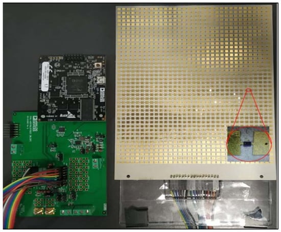
Figure 1.
The IRS prototype with 40 × 33 unit cells allows a tunable one-dimensional control of the reflected beam in the X-Band and Ku-band [29]. Control of the reflected beam in 1D was achieved with 32 D/A voltages applied to each of its 33 columns.
For example, in [29], a metasurface with 40 × 33-unit cells that allow a tunable one-dimensional control of the reflected beam in the X-Band and Ku-Band is demonstrated. A varactor diode model of MACOM MAVR–011020-11411 was used as a tunable component. By using 32 channels of D/A for each of the 32 columns of varactors in this metasurface, the metasurface is controlled in 1D mode. A photo of this IRS is shown in Figure 1.
In the above example, 32 digital-to-analog converters (DACs) varying from 0 to 20 V were wired to each column independently, yielding a capacitance gradient only along the X-axis. Thus, the steering is only possible on the X-axis. Simulation results at 11 GHz, 12 GHz and 13.5 GHz of this design for steering angles of 10°, 30° and 50° are given in [29]. By varying the bias voltages of the varactor diodes between the 33 columns of the metasurface, different Δφx (see Equation (1)) can be applied along the X-direction. Such operation allows the steering of the reflected beam to different angles, θ, at the same frequency. The reflected wavefronts are shown in Figure 2.
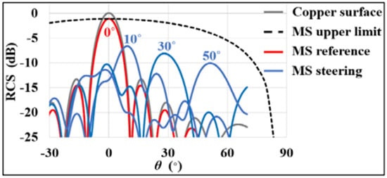
Figure 2.
Far-field simulation results for metasurface reflector at 11 GH [29].
Two-dimensional beam steering requires, in the above case, a total number of 40 × 32 DACs, one DAC for each varactor on the metasurface. This significantly complicated the wiring and the design of the control system of that IRS. Furthermore, such a complicated design may degrade the steering performance and an RF circuit should be added, increasing the manufacturing cost.
On the other hand, the discrete or “digital coding” method can be implemented for IRS beam steering based on the metasurface [32,33,34,35,36,37]. A common component for implementing a digital coding metasurface is the PIN switch diode since it is very inexpensive and can be easily placed on surfaces of standard PCB manufacturing. Each unit cell of the metasurface, integrated with one PIN switch, enables two different phase modes (1-bit resolution) 0° and 180°. If two PIN switches per unit cell are used, four different phase modes (2-bit resolution), 45°, 135°, 225° and 315°, can be realized. In those cases, each PIN diode can be modeled as a lumped element with two or four fixed capacitance values. For example, in [34,35], a 1-bit resolution metasurface for X-band is demonstrated. Each unit cell is integrated with one PIN switch operating in two reflected phases (states) with a difference of 180° between the states, realizing a 1-bit digital unit cell.
According to [32], a phase difference of 180° was obtained at 8.6 GHz. A unit cell with the desired reflection phase value of 0° up to 180° will be set to digital value ‘0’, and a unit cell with desired reflection phase value between 180° to 360° will be set to digital value ‘1’. The unit cell state of each column of the metasurface was defined independently, and 1D beam steering was achieved.
Implementing a 1-bit phase control metasurface is easier than a continuous phase control metasurface. The latter improves the beam steering performance by about 3.5 dB compared to the 1-bit phase control [14]. In addition, there is a disadvantage in the context of energy consumption is the DC bias for the ‘ON’ state in the PIN switch, which is not negligible for a metasurface with many unit cells, given the statistical assumption that half of the unit cells on the surface are in the ‘ON’ state [36].
In the above examples, a complicated control system is needed for DC biasing, whether using a continuous or discrete phase control metasurface. This system can be based on an FPGA, microcontroller board, connectors, RF chokes, radial stubs and parallel DACs [14,34,35]. Additionally, additional PCB layers are needed for the DC biasing of the metasurface. For a larger metasurface, those difficulties become dominant and may degrade the RF performance due to the density of the electric circuit on the backside of the metasurface [14]. The complexity of using wires and circuits to achieve beam steering has been shown in many studies. References for some of those studies are given in [14,15,16,27,28,29,30,31,32,33,34,35,36,37,38,39]. For the case of discrete phase control, this leads to the degeneration of the implementation to only 1-bit phase control due to the cost and complexity of using a high number of DACs. Examples of those complex control circuits for the 1-bit phase control metasurface are given in [34] for 10 × 10 unit cells and in [35] for 14 × 14 unit cells. In those examples, only a relatively small-sized metasurface with up to several hundreds of unit cells is demonstrated. In addition, the margins are added to the effective metasurface area for the placements of the connectors used for DC bias control. This decreases the aperture efficiency of the metasurface.
In the next section, we suggest a new and very promising technology in which no wires nor RF circuits are required, namely SBI. As the number of unit cells required to implement a metasurface increase, the more complex and expensive it becomes. A 2D beam steering using the standard DC biasing technology becomes more complex and expensive. It requires many controlled DC sources, RF chokes and a complex board. This paper demonstrates 1D and 2D continuous reflection phase beam steering with a large metasurface composed of 14 × 120 unit cells and 60 × 60 unit cells. Implementing such an IRS is arduous to design, manufacture and control. The SBI technology suggested here significantly simplifies the metasurface control design by replacing it with a standard image projector. The SBI technology is shown here to solve the limitation of implementing a larger area metasurface with many unit cells. In the next section. The SBI technology presented here significantly simplifies the metasurface control design by replacing it with a standard image projector. The SBI technology is shown here to solve the limitation of implementing a larger area metasurface with many unit cells.
3. Steer by Image Technology
The tunable component that is suggested to be embedded in the design of the metasurface unit cell, realizing the SBI technology, is a PIN photodiode. PIN diodes in general [40] and PIN photodiodes are used extensively in RF and microwave photonic communication applications [41]. Discrete or digital metasurfaces based on a PIN diode were designed and experimentally tested, and a two-state 1-bit control [34,35] and four-state 2-bit control metasurface was also demonstrated [42].
Here, we design a reconfigurable discrete or continuous unit cell based on a PIN photodiode. Using a PIN photodiode as a tunable component in the unit cell has the following advantages: (1) It can operate in an open circuit mode with very low energy consumption relative to PIN diode; (2) High-speed response; (3) High sensitivity to light; (4) Very inexpensive; (5) Long lifetime; (6) Its internal junction capacitance, Cj, is controlled by the incident light intensity impinging onto the PIN photodiode [41]. Experimental results of a commercial PIN photodiode (Vishay Semiconductors BVP10 [43]) showing the influence of the projection light color and intensity on the PIN photodiode’s junction capacitance are given in Figure 3 [43].
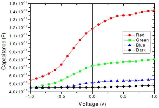
Figure 3.
Capacitance–voltage characteristics of a commercial PIN photodiode (Vishay Semiconductors BVP10), under dark conditions and under illumination with different wavelengths (red, green and blue) which is analog to three different intensities due to high quantum efficiency at red light compared to green light and blue light, respectively [44].
In an open circuit PIN photodiode (I = 0) operation, the projected light generates electrons and holes flowing to the n- and p-type sides of the junction, narrowing the depletion region and increasing the junction capacitance Cj. Figure 3 gives the total photodiode capacitance, Cpd depending on the color of the light incident on the photodiode. In this case, the dynamic range of the total photodiode capacitance Cpd is 4.5–12 pF without DC biasing (I = 0).
To realize an IRS based on a reconfigurable metasurface with a PIN photodiode as a tunable element, the PIN photodiode must be located on the backside of the metasurface. This will enable a convenient and flexible projection of the light onto each PIN photodiode changing its junction capacitance, Cj, as required. A similar geometry, in which the tunable element is located on the backside of an entire Ku-band metasurface board, was suggested by us in [28]. In this study, a varactor diode was located on the backside of such a metasurface, demonstrating a very good beam reflection performance compared to typical geometry in which the varactor diode is located on the frontside of the metasurface. This new geometry design in which the varactor diodes are located on the backside of the reflector eliminates the absorbance and scattering by the varactor diode on the reflected radiation. The alternative solution of using larger unit cells and diodes on the frontside [45] suffers from low resolution and limited performance due to scan loss which increases for large-sized unit cells [46]. In the new geometry, shown in Figure 4, improved performances of the reflected beam were achieved.
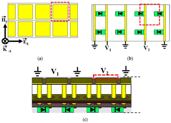
Figure 4.
Design of the metasurface reflector structure with varactor diodes DC stimulations circuit. (a) Frontside with the structure of rectangular metal patches array; (b) Backside with DC voltage and diode polarization; (c) Three-dimensional inside view of the electrical circuit for each diode [28].
The design of the SBI metasurface is based on the geometry and structure shown in Figure 4, but with PIN photodiodes instead of the varactor. As explained, the design of the SBI metasurface is based on PIN photodiodes as tunable elements operating in open circuit mode. No DC stimulation is required in this operating mode, simplifying the design and eliminating the need for an FPGA board and wire connections. Figure 5 illustrates the concept of SBI technology.
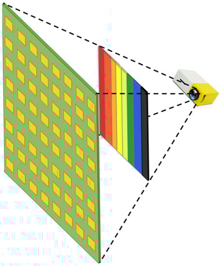
Figure 5.
The proposed concept of Steer by Image technology (SBI). In this concept, a projector illuminates the backside of the metasurface with the desired color patterns, which changes the capacitance of the photodiodes and steers the beam in the desired direction.
The SBI configuration suggested in Figure 5 requires an image to be projected on the backside of the metasurface. One- or two-dimensional beam steering or other beam manipulation such as focus can be realized by a projection image with appropriate light and color levels on the metasurface backside, as shown in Figure 5. The color pixel changes between the columns and rows determine the beam steering angle or other beam manipulation of the IRS. No FPGA board nor DC biasing circuit are required in SBI technology IRS. A simple and compact image projector [47] is needed to project an image on the metasurface backside of such IRS.
Using SBI technology, a 2D beam steering for a variety of wavefronts can be implemented. Additionally, discrete or digital coding patterns can be easily projected on the backside of the metasurface, creating any required beam steering, θ, and for any incidence, wavefront beam demonstrated in [36,37].
4. Unit Cell and Metasurface Design
The unit cell configuration suggested for SBI technology where the tunable element, a photodiode, is located on the backside of the metasurface [28] is shown in Figure 6. The photodiode used is AMS OSRAM SFH2704 [48] which has very similar properties to Vishay Semiconductors BVP10 [43] and offers a good capacitance response to the light color as shown in Figure 3.
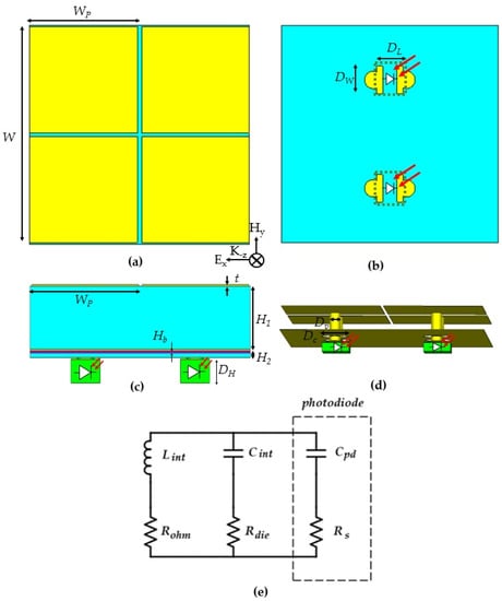
Figure 6.
Design of the unit cell: (a) Frontside; (b) Backside; (c) Side view of the layers’ structure; (d) Three-dimensional view of the inner unit cell; (e) Cell equivalent circuit configuration suggested for SBI technology.
In Figure 6b, the PIN photodiode is connected between two adjacent patches on the backside of the metasurface. Two PIN photodiodes are used in each unit cell for more capacitance uniformity throughout the unit cell. Figure 6e shows the electrical equivalent circuit for the unit cell. The losses of the metasurface are a result of the resistances of the dielectric substrate () and Cooper’s (). The unit cell parameter values are determined by the unit cell’s material, dimensions and geometry. As a rule of thumb, Cint is proportional to the metal area of the unit cell and Lint to its thickness [28].
A simplified illustration of a small-sized metasurface in the SBI technology is shown in Figure 7.
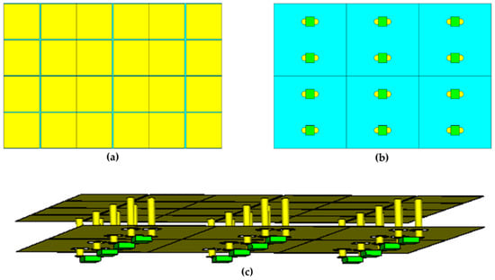
Figure 7.
Three-dimensional structure of the SBI metasurface: (a) Frontside; (b) Back side; (c) Side view of the layers’ structure.
The PIN photodiode of Figure 3 has a capacitance dynamic range contribution in zero bias. The unit cell parameters and the metasurface parameters are given in Table 1.

Table 1.
Unit cell dimension parameters.
The simulated photodiode parameters for the unit cell reflection are shown in Table 2.
Table 2.
Simulated photodiode parameters.
The unit cell simulation results were based on CST simulation code. The magnitude and phase reflection as a function of frequency for three capacitance values are shown in Figure 8 for min= 4.5 pF, max = 12 pF and for = 5.45 pF, which leads to resonance frequency at 1 GHz.
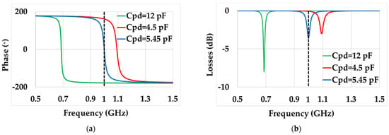
Figure 8.
Unit cell results. (a) Phase. (b) Magnitude.
The results in Figure 8a show a dynamic phase range of about 340°. The maximum unit cell loss at the operation frequency is for the capacitance of and is about 4 dB.
Investigating the capacitance as a function of a reflected phase at 1 GHz will provide beam steering using SBI technology (see Figure 3). The capacitance between min and max can be converted to light color.
Figure 9 shows that by using the PIN photodiode of AMS OSRAM SFH2704, a high tunning of the reflection phase can be achieved. The data shown in Figure 8 were used to plan the phase distribution on the metasurface, thus reconfiguring the metasurface for 1D and 2D beam steering at 1 GHz. Higher frequencies can also be accomplished using PIN photodiodes with lower capacitance [28].
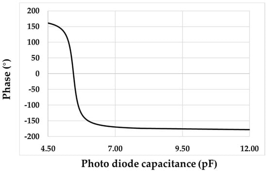
Figure 9.
Reflected phase at 1 GHz as a function of the photodiode capacitance, Cpd.
5. One-Dimensional and Two-Dimensional Far-Field Results
The far-field results were simulated for a metasurface with 14 × 120 cells. The 1D beam steering results are shown in Figure 10a and the 2D color pattern with column change only is shown in Figure 10b, respectively.
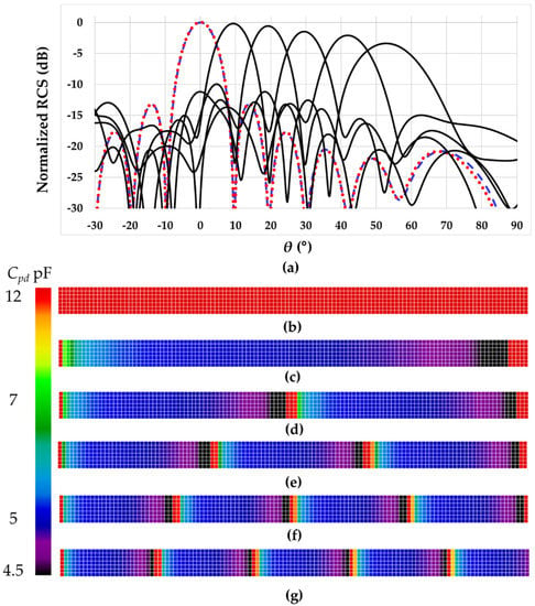
Figure 10.
The IRS far-field simulation results. The beam steering angles of about 10°, 20°, 30°, 40° and 50° degrees and the reference cases for 0° are shown in (a), and the corresponding projection patterns that were used for the beam steering are shown in (b–g). The metasurface simulations were carried out with a metasurface size of 14 × 120 cells. In (a), the red line is for constant photodiodes capacitance and the blue graph is for a metal copper plate as a reference.
As shown in Figure 10 to demonstrate beam steering ability in the X-axis direction, the number of rows (Y-axis) was decreased significantly to save on simulation execution time.
The 2D beam steering was also simulated with 60 × 60 cells for symmetry in both dimensions and the far-field result is shown in Figure 11.
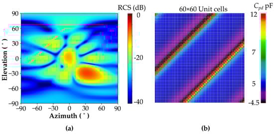
Figure 11.
(a) shows a 2D beam steering with an angle of 30° in the azimuth direction and −30° in the elevation direction. (b) shows the projection pattern used for this 2D beam steering.
As shown in Figure 11, the simulation result is a steering angle of 30°and −30° in the azimuth and elevation directions, with high-quality 2D beam steering obtained. The beam steering result is according to the desired angle when the phase gradient is on both the X-axis and Y-axis, as seen in Figure 11b. In addition, as shown in Figure 9 and Figure 10, in all the projection patterns, the dominant pixel color is blue, representing the Cpd value of around 5 pF. This is because the dynamic reflection phase mostly concentrates about 5 pF, making the blue color dominant (see Figure 3 and Figure 10). The greater the beam steering is to a larger angle, the denser and more cyclic the pixel pattern is, as shown in Figure 10b–g.
6. Conclusions
The complexity of using wires and circuits to achieve beam steering has been shown in many studies. References for some of those studies are given in [14,15,16,27,28,29,30,31,32,33,34,35,36,37,38,39]. This paper demonstrated 1D and 2D continuous reflection phase beam steering with a metasurface size of 14 × 120 and 60 × 60 unit cells. The SBI technology suggested here significantly simplifies the metasurface control design by replacing it with a standard image projector. For a traditional 60 × 60 unit cell metasurface to operate in 2D, 3600 different DC analog outputs are required. Thus, it is a very complex and very impractical circuit. SBI technology eliminates the need for many DACs cards, digital output and other components used in other studies [14,15,16,27,28,29,30,31,32,33,34,35,36,37,38]. Instead, an image can be projected to the backside of the metasurface, where the PIN photodiodes are located (see Figure 5). The projected image controls the junction capacitance of the PIN photodiode, which changes the reflected beam phase accordingly (see Figure 8).
Furthermore, a complete unit cell design for an operating frequency of 1 GHz was carried out. Finally, a far-field beam steering simulation of a large metasurface of 14 × 120 unit cells for 1D and 60 × 60 unit cells for 2D was demonstrated. Quality beam steering results with up to 50° for 1D and 30° in the azimuth and −30° in the elevation for 2D were shown. The simulations performed in this case were very heavy and required a long calculation time. Beam steering at higher frequencies can also be achieved if the PIN photodiode has lower total capacitance.
Author Contributions
Conceptualization, D.R. (David Rotshild), A.A.; Methodology, D.R. (David Rotshild); software, D.R. (David Rotshild), D.R. (Daniel Rozban), E.R., A.B., R.Y. and L.B.; validation, D.R. (David Rotshild), D.R. (Daniel Rozban), E.R., A.B., R.Y. and L.B.; formal analysis, D.R. (David Rotshild), D.R. (Daniel Rozban); investigation, D.R. (David Rotshild), D.R. (Daniel Rozban); resources, D.R. (David Rotshild), D.R. (Daniel Rozban); data curation, D.R. (David Rotshild), E.R., A.B., R.Y. and L.B.; writing—D.R. (David Rotshild), D.R. (Daniel Rozban) and A.A.; writing—review and editing, D.R. (David Rotshild), D.R. (Daniel Rozban) and A.A.; visualization, D.R. (David Rotshild), D.R. (Daniel Rozban); supervision, D.R. (David Rotshild), D.R. (Daniel Rozban) and A.A.; project administration, D.R. (David Rotshild), D.R. (Daniel Rozban) and A.A.; funding acquisition, D.R. (Daniel Rozban) and A.A. All authors have read and agreed to the published version of the manuscript.
Funding
This research received no external funding.
Institutional Review Board Statement
Not applicable.
Informed Consent Statement
Not applicable.
Data Availability Statement
Not applicable.
Conflicts of Interest
The authors declare no conflict of interest.
References
- Vesselago, V.G. The electrodynamics of substances with simultaneously negative values of permittivity and permeability. Sov. Phys. Usp. 1968, 10, 509–514. [Google Scholar] [CrossRef]
- Shelby, R.A.; Smith, D.R.; Schultz, S. Experimental verification of a negative index of refraction. Science 2001, 292, 77–79. [Google Scholar] [CrossRef] [PubMed] [Green Version]
- Caloz, C.; Itoh, T. Application of the transmission line theory of left-handed (LH) materials to the realization of a microstrip “LH line”. In Proceedings of the IEEE Antennas and Propagation Society International Symposium (IEEE Cat. No. 02CH37313), San Antonio, TX, USA, 16–21 June 2002; Volume 2, pp. 412–415. [Google Scholar]
- Tao, H.; Landy, N.I.; Bingham, C.M.; Zhang, X.; Averitt, R.D.; Padilla, W.J. A metamaterial absorber for the terahertz regime: Design, fabrication and characterization. Opt. Express 2008, 16, 7181–7188. [Google Scholar] [CrossRef] [PubMed]
- Landy, N.; Smith, D.R. A full-parameter unidirectional metamaterial cloak for microwaves. Nat. Mater. 2013, 12, 25–28. [Google Scholar] [CrossRef]
- Gil, L.; David, R.; Amir, A. Flat mirror for millimeter-wave and terahertz imaging systems using an inexpensive metasurface. Chin. Opt. Lett. 2017, 15, 011101. [Google Scholar]
- Ma, Q.; Shi, C.B.; Chen, T.Y.; Qi, M.Q.; Li, Y.; Cui, T.J. Broadband metamaterial lens antennas with special properties by controlling both refractive-index distribution and feed directivity. J. Opt. 2018, 20, 045101. [Google Scholar] [CrossRef]
- Zou, X.; Zheng, G.; Yuan, Q.; Zang, W.; Zhu, S. Imaging based on metalenses. PhotoniX 2020, 1, 2. [Google Scholar] [CrossRef] [Green Version]
- Ma, Q.; Shi, C.B.; Bai, G.D.; Chen, T.Y.; Noor, A.; Cui, T.J. Beam-Editing Coding Metasurfaces Based on Polarization Bit and Orbital-Angular-Momentum-Mode Bit. Adv. Opt. Mater. 2017, 5, 1700548. [Google Scholar] [CrossRef]
- Qiao, Z.; Wan, Z.; Xie, G.; Wang, J.; Fan, D. Multi-vortex laser enabling spatial and temporal encoding. PhotoniX 2020, 1, 13. [Google Scholar] [CrossRef]
- Wu, Q.; Zhang, R. Intelligent Reflecting Surface Enhanced Wireless Network via Joint Active and Passive Beamforming. IEEE Trans. Wirel. Commun. 2019, 18, 5394–5409. [Google Scholar] [CrossRef] [Green Version]
- Zhang, X.G.; Tang, W.X.; Jiang, W.X.; Bai, G.D.; Tang, J.; Bai, L.; Qiu, C.; Cui, T.J. Light-Controllable Digital Coding Metasurfaces. Adv. Sci. 2018, 5, 1801028. [Google Scholar] [CrossRef] [PubMed]
- Zhang, X.G.; Jiang, W.X.; Jiang, H.L.; Wang, Q.; Tian, H.W.; Bai, L.; Luo, Z.J.; Sun, S.; Luo, Y.; Qiu, C.; et al. An optically driven digital metasurface for programming electromagnetic functions. Nat. Electron. 2020, 3, 165–171. [Google Scholar] [CrossRef]
- Han, J.; Li, L.; Liu, G.; Wu, Z.; Shi, Y. A Wideband 1 bit 12 × 12 Reconfigurable Beam-Scanning Reflectarray: Design, Fabrication, and Measurement. IEEE Antennas Wirel. Propag. Lett. 2019, 18, 1268–1272. [Google Scholar] [CrossRef]
- Turpin, J.P.; Bossard, J.A.; Morgan, K.L.; Werner, D.H.; Werner, P.L. Reconfigurable and Tunable Metamaterials: A Review of the Theory and Applications. Int. J. Antennas Propag. 2014, 2014, 429837. [Google Scholar] [CrossRef]
- Bao, L.; Cui, T.J. Tunable, reconfigurable, and programmable metamaterials. Microw. Opt. Technol. Lett. 2019, 62, 9–32. [Google Scholar] [CrossRef]
- Palma, L.D.; Clemente, A.; Dussopt, L.; Sauleau, R.; Potier, P.; Pouliguen, P. Circularly-Polarized Reconfigurable Transmitarray in Ka-Band with Beam Scanning and Polarization Switching Capabilities. IEEE Trans. Antennas Propag. 2017, 65, 529–540. [Google Scholar] [CrossRef]
- Chen, L.; Ma, H.L.; Cui, H.Y. Wavefront manipulation based on mechanically reconfigurable coding metasurface. J. Appl. Phys. 2018, 124, 043101. [Google Scholar] [CrossRef]
- Rotshild, D.; Rahamim, E.; Abramovich, A. Innovative reconfigurable metasurface 2-D Beam-Steerable reflector for 5G wireless communication. Electronics 2020, 9, 1191. [Google Scholar] [CrossRef]
- Savo, S.; Shrekenhamer, D.; Padilla, W.J. Liquid Crystal Metamaterial Absorber Spatial Light Modulator for THz Applications. Adv. Opt. Mater. 2014, 2, 275–279. [Google Scholar] [CrossRef]
- Foo, S. Liquid-crystal-tunable metasurface antennas. In Proceedings of the 2017 11th European Conference on Antennas and Propagation (EUCAP), Paris, France, 19–24 March 2017. [Google Scholar]
- Deng, L.; Teng, J.; Liu, H.; Wu, Q.Y.; Tang, J.; Zhang, X. Direct Optical Tuning of the Terahertz Plasmonic Response of InSb Subwavelength Gratings. Adv. Opt. Mater. 2013, 1, 128–132. [Google Scholar] [CrossRef]
- Singh, R.; Plum, E.; Zhang, W.; Zheludev, N.I. Highly tunable optical activity in planar achiral terahertz metamaterials. Opt. Express 2010, 18, 13425–13430. [Google Scholar] [CrossRef] [PubMed]
- Yaghmaee, P.; Karabey, O.H.; Bates, B.; Fumeaux, C.; Jakoby, R. Electrically Tuned Microwave Devices Using Liquid Crystal Technology. Int. J. Antennas Propag. 2013, 2013, 824214. [Google Scholar] [CrossRef] [Green Version]
- Momeni Hasan Abadi, S.M.A.; Booske, J.H.; Behdad, N. MAcro-Electro-Mechanical Systems (MÆMS) based concept for microwave beam steering in reflectarray antennas. J. Appl. Phys. 2016, 120, 054901. [Google Scholar] [CrossRef]
- Vassos, E.; Churm, J. Alexandros Feresidis Ultra-low-loss tunable piezoelectric-actuated metasurfaces achieving 360° or 180° dynamic phase shift at millimeter-waves. Sci. Rep. 2020, 10, 15679. [Google Scholar] [CrossRef]
- Rotshild, D.; Abramovich, A. Realization and validation of continuous tunable metasurface for high resolution beam steering reflector at K-band frequency. Int. J. RF Microw. Comput. Aided Eng. 2021, 31, e22559. [Google Scholar] [CrossRef]
- Rotshild, D.; Abramovich, A. Wideband reconfigurable entire Ku-band metasurface beam-steerable reflector for satellite communications, IET Microw. Antennas Propag. 2019, 13, 334–339. [Google Scholar]
- Rotshild, D.; Abramovich, A. Ultra-Wideband reconfigurable X-band and Ku-band metasurface beam-steerable reflector for satellite communications. Electronics 2021, 10, 2165. [Google Scholar] [CrossRef]
- Rotshild, D.; Abramovich, A. Polarization consideration of 2-D beam-steering metasurface reflector at Ka-band for wireless communication. In Proceedings of the 2021 IEEE International Conference on Microwaves, Antennas, Communications and Electronic Systems (COMCAS), Tel Aviv, Israel, 1–3 November 2021; pp. 486–490. [Google Scholar]
- Rahamim, E.; Rotshild, D.; Abramovich, A. Performance Enhancement of Reconfigurable Metamaterial Reflector Antenna by Decreasing the Absorption of the Reflected Beam. Appl. Sci. 2021, 11, 8999. [Google Scholar] [CrossRef]
- Cui, T.J.; Qi, M.Q.; Wan, X.; Zhao, J.; Cheng, Q. Coding metamaterials, digital metamaterials and programmable metamaterials. Light Sci. Appl. 2014, 3, e218. [Google Scholar] [CrossRef]
- Du, B. Analysis and Design of Simple, Low Loss and Low Cost Reconfigurable Reflect Arrays. Doctoral Dissertation, University of Toronto, Toronto, ON, Canada, 2017. [Google Scholar]
- Yang, H.; Yang, F.; Xu, S.; Mao, Y.; Li, M.; Cao, X.; Gao, J. A 1-Bit 10 × 10 Reconfigurable Reflect array Antenna: Design, Optimization, and Experiment. IEEE Trans. Antennas Propag. 2016, 64, 2246–2254. [Google Scholar] [CrossRef]
- Zhang, H.; Chen, X.; Wang, Z.; Ge, Y.; Pu, J. A 1-Bit Electronically Reconfigurable Reflect array Antenna in X Band. IEEE Access 2019, 7, 66567–66575. [Google Scholar] [CrossRef]
- Yang, H.; Cao, X.; Yang, F.; Gao, J.; Xu, S.; Li, M.; Chen, X.; Zhao, Y.; Zheng, Y.; Li, S. A programmable metasurface with dynamic polarization, scattering and focusing control. Sci. Rep. 2016, 6, 35692. [Google Scholar] [CrossRef] [PubMed] [Green Version]
- Amri, M.M.; Tran, N.M.; Park, J.H.; Kim, D.I.; Choi, K.W. A Programmable Binary Metasurface for Wireless Power Transfer Application. In Proceedings of the 2020 IEEE Wireless Power Transfer Conference (WPTC), Seoul, Korea, 15–19 November 2020; pp. 334–337. [Google Scholar]
- Ran, N.M.; Amri, M.M.; Park, J.H.; Hwang, S.I.; Kim, D.I.; Choi, K.W. A Novel Coding Metasurface for Wireless Power Transfer Applications. Energies 2019, 12, 4488. [Google Scholar]
- Ratni, B.; de Lustrac, A.; Piau, G.P.; Burokur, S.N. Active metasurface for reconfigurable reflectors. Appl. Phys. A 2018, 124, 104. [Google Scholar] [CrossRef]
- Microsemi-Watertown Company. The PIN Diode Circuit Designers’ Handbook; Microsemi Corporation: Watertown, MA, USA, 1998. [Google Scholar]
- Sun, K.; Beling, A. High-Speed Photodetectors for Microwave Photonics. Appl. Sci. 2019, 9, 623. [Google Scholar] [CrossRef] [Green Version]
- Huang, C.; Sun, B.; Pan, W.; Cui, J.; Wu, X.; Luo, X. Dynamical beam manipulation based on 2-bit digitally-controlled coding metasurface. Sci. Rep. 2017, 7, 42302. [Google Scholar] [CrossRef] [Green Version]
- PIN Photo Diode BVP 10 Datasheets. Available online: https://www.vishay.com/ppg?81502 (accessed on 31 December 2021).
- Dora Gonçalves, L.; Fernandes, M.; Louro, P.; Vieira, M.; Fantoni, A. Measurement of Photo Capacitance in Amorphous Silicon Photodiodes. In Proceedings of the 4th Doctoral Conference on Computing, Electrical and Industrial Systems (DoCEIS), Costa de Caparica, Portugal, 15–17 April 2013; pp. 547–554. [Google Scholar] [CrossRef]
- Nie, J.; Tan, Y.Q.; Ji, C.L.; Liu, R. Analysis of Ku-band steerable metamaterials reflectarray with tunable varactor diodes. In Proceedings of the Electromagnetic Research Symposium (PIERS), Shanghai, China, 8–11 August 2022; pp. 709–713. [Google Scholar]
- Bhattacharyya, A.K. Phased Array Antennas: Floquet Analysis, Synthesis, BFNs and Active Array Systems; John Wiley & Sons Press: New York, NY, USA, 2006; pp. 13–14, 18–21. [Google Scholar]
- A Commercial Compact Projector. Available online: https://projectorninja.com/aaxa-p7-hd-projector-review/ (accessed on 31 December 2021).
- Osram Chip LED, SFH 2704 Datasheet. Available online: https://www.osram.com/ecat/com/en/class_pim_web_catalog_103489/prd_pim_device_6230418/#62a1fdff42f13778e2055fdc87c50fcb (accessed on 31 December 2021).
Publisher’s Note: MDPI stays neutral with regard to jurisdictional claims in published maps and institutional affiliations. |
© 2022 by the authors. Licensee MDPI, Basel, Switzerland. This article is an open access article distributed under the terms and conditions of the Creative Commons Attribution (CC BY) license (https://creativecommons.org/licenses/by/4.0/).