Article

A Facile Centrifuge Coating Method for High-Performance CsPbBr3 Compact and Crack-Free Nanocrystal Thin Film Photodetector

International Training Institute for Materials Science (ITIMS), Hanoi University of Science and Technology (HUST), Hanoi 10000, Vietnam
*
Author to whom correspondence should be addressed.
Crystals 2022, 12(5), 587; https://doi.org/10.3390/cryst12050587
Submission received: 23 March 2022 / Revised: 18 April 2022 / Accepted: 20 April 2022 / Published: 22 April 2022
(This article belongs to the Special Issue Metal–Semiconductor Photodetector)

Abstract

:
All-inorganic perovskite quantum dots (QDs), a promising semiconductor material, is suitable for new generation optoelectronic application. While there are many kinds of coating procedures for producing perovskite QDs peorovskite film, those methods require post-treatments and an additional dispersion support agent while still retaining pinholes and cracks. In this work, we report a facile method to produce CsPbBr3 film on a pre-patterned Pt electrode using a centrifuge coating method for photodetector (PD) application. Compact and crack-free films with ~500 nm thick from various particle sizes of 8 nm, 12 nm, and >30 nm were achieved with a suitable ratio of toluene/ethyl acetate solvent for visible light photodetector application. The optimized device has an on/off ratio of 103, detectivity of 3 × 10¹² Jones, and responsivity of 6 A/W. In comparison, the on/off ratio of the device fabricated by the centrifuge coating method was 102 times higher than by the drop-coating method. The PD performance exhibited considerable moisture stability at mild high ambient temperature with no encapsulation for more than two weeks. The results suggest that this is a potential method for fabricating all inorganic perovskite nano-semiconductor films for further optoelectronic application in photodetectors, LEDs, and solar cells.

1. Introduction

The rapid improvement of the fabricating methods of all-inorganic pervovskite has led to a remarkable improvement of its optoelectronic applications such as solar cell, light emitting diode, photodetector, and so on [1,2,3]. For example, in solar cell application, a variety of photovoltaic technologies for light harvesting have been employed to date. They are classified based on photoactive layers, including silicon solar cell, thin film solar cell (e.g., gallium arsenide and copper indium gallium selenide), and some emerging PV tecnologies, such as organic photovoltaic (OPV) [4,5], sensitization-based solar cells [6], and perovskite solar cells [7]. Among these, perovskite solar cell is a promising candidate due to the high light-absorption coefficient, long carrier diffusion length, and solution processibility of metal halide perovskite materials [7]. Because the bulk perovskite crystals exhibit poor phase stability due to the weak ion bonding nature easily leading to phase separation [8,9], by reducing the size of crystals, the performance of perovskite nanocrystal (PVK NC)-based devices was largely improved due to reduced crystal strain resulting in their good phase stability, narrow PL emission, tunable light absorption spectrum, and high photoluminescence quantum yield (PLQY) in comparison with bulk counterparts [10,11,12]. The all-inorganic perovskite quantum dots are one of next generation semiconductor materials which are currently of great interest for solar cell application because they are more durable than other hybrid perovskite materials. The power conversion efficiency of PQDSCs was significantly increased from 10.77% to 17.39% (certified 16.6%) by the control fine surface chemistry of PQDs and the device physics of PQDSCs [13,14]. Despite extensive research efforts, the efficiency of the PSCQSC device is still below that of other hybrid perovskite materials with the highest conversion efficiency of 25.17% [15]. Therefore, there is an important interest in further boosting the performance of fully inorganic PQDSCs through optimizing the synergies of films and device interfaces. Generally, the as-prepared PVK NCs using a solution process are usually coated with an insulating nature of long chain-ligand which makes it difficult to directly apply in optoelectronic devices. Thus, after fabrication, it requires a purification procedure for removing excess ligands and enhancing the opto-electronic performance [16,17]. Various PVK NC films have been successfully prepared by diverse coating methods, including spin coating, spray coating, dip-coating, and so on [18,19,20,21]. Several studies have reported on CsPbBr3 NC film-based optoelectronic devices [21,22,23,24,25]. A large amount of residual solvent, problems adjusting viscosity, retaining pinholes, and cracks are major drawbacks of these methods. Lack of electrical connectivity within NC film, poor adhesion of the NC film to the substrate, and the requirement for post-treatment methods to provide conductive networks are further limitations of the above-mentioned approaches.
Recently, a high-speed centrifuge coating process was introduced for CNT, Ag nanowires, as well as CsPbBr3 PVK NC film with long-term stability optoelectronic devices [25,26,27,28]. This technique relies on centrifugal force to form a uniform layer on the substrate surface perpendicular to the force, resulting in a closely packed nanomaterial film. Here, we demonstrate the fabrication of various particle size films of CsPbBr3 NCs via the centrifuge coating method with a suitable ratio of toluene/ethyl acetate solvent for visible light photodetector application. The structural, photoluminescence properties and I–V performance of the CsPbBr3 NC film photodetectors are also presented.

2. Materials and Methods

Materials: All reagents were used without further purification. Lead bromide (PbBr2, 99.9% metal basis), cesium carbonate (Cs2CO3, 99.9% metal basis), oleylamine (OAm, 80–90%), oleic acid (OA, analytical grade), octandecene, ethyl acetate, and toluene (>99%, analytical grade) were bought from Macklin Chemical.
CsPbBr3 NCs fabrication by hot injection method: Firstly, the Cs Oleate precusor was prepared by mixing 120 mg of Cs2CO3, 0.5 mL OA, and 5 mL ODE in a 50 mL three-necked flask, and heated at 120 °C until Cs2CO3 powder was completely dissolved. The precursor solution was maintained at 120 °C before use. Next, 70 mg PbBr2 with 0.5 mL OA, 0.5 mL OLA, and 5 mL ODE was heated at 140 °C with magnetic stirring until completely dissolved. For CsPbBr3 fabrication, there was rapid injection of 0.5 mL of Cs-oleate precursor remains at 120 °C into the PbBr2 precursor at 120, 140, and 160 °C and stirring continued for 1 min. The solution after stirring was immediately soaked in ice water.
Centrifuge coating CsPbBr3 NC film on Pt electodes: The planar integrated Ti/Pt (50/200 nm) electrode is fabricated using standard photolithography to pattern the photoresist for subsequent metallization and lift-off. The electrode included 40 fingers with the channel width and length of 20 μm and 1.60 mm, respectively. The total active area was 0.128 mm2.
Prior to coating, pre-patterned Pt electrodes on the SiO2/Si substrate were ultrasonically cleaned in acetone and ethanol for 10 min and dried in an oven at 100 °C for 30 min. Samples were placed vertically into a 0.5 cm diameter centrifuge tube. Before coating, 1 mL crude CsPbBr3 NCs was washed by adding 1 mL ethyl acetate and centrifuged at 15,000 rpm for the removal of all excess organic agents such as ODE, OA, OLA. The supernatant was discarded and the particles were redispersed in toluene/ethyl acetate mixed solvent. Then, centrifuge coating was carried out with pre-patterned Pt electrodes faced with the direction of applied centrifuge force with CsPBr3 NCs dispersed in toluene/ethyl acetate mixed solvent at a rotational speed of 15,000 rpm for 15 min. The resulting substrate was gently removed from the tube and dried at ambient air temperature to completely evaporate any remaining solvent.

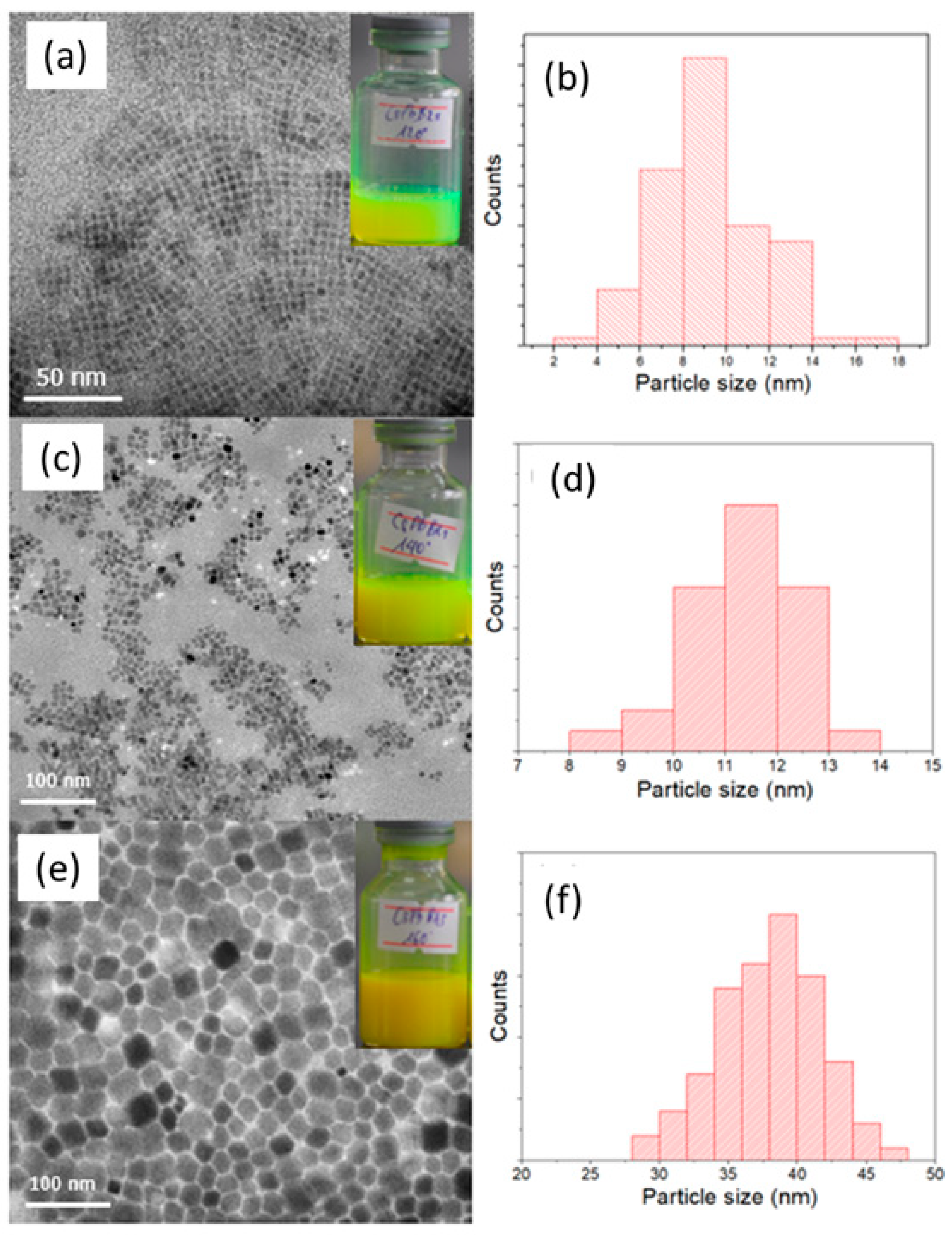
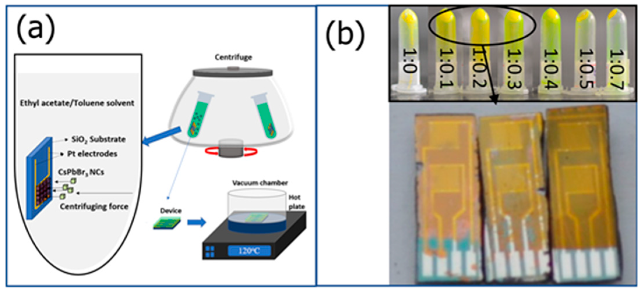
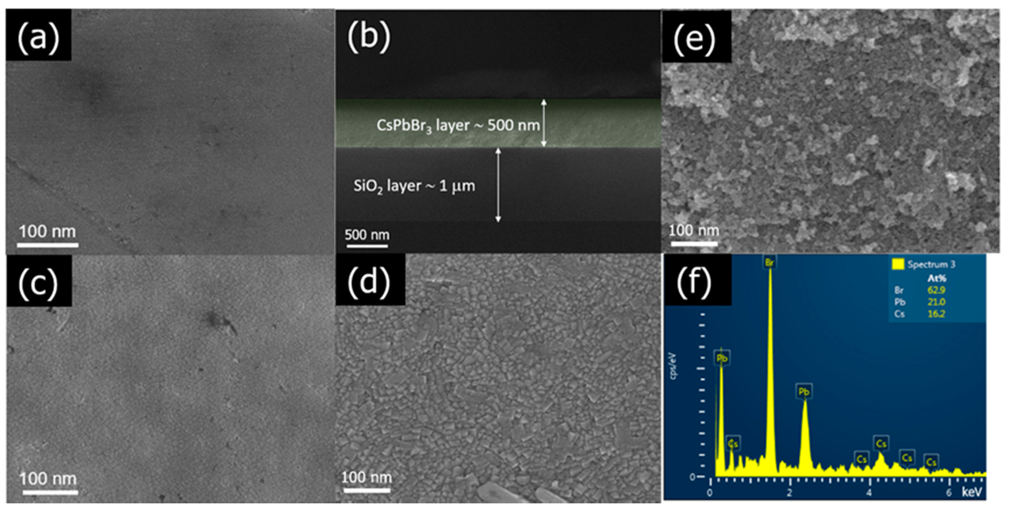
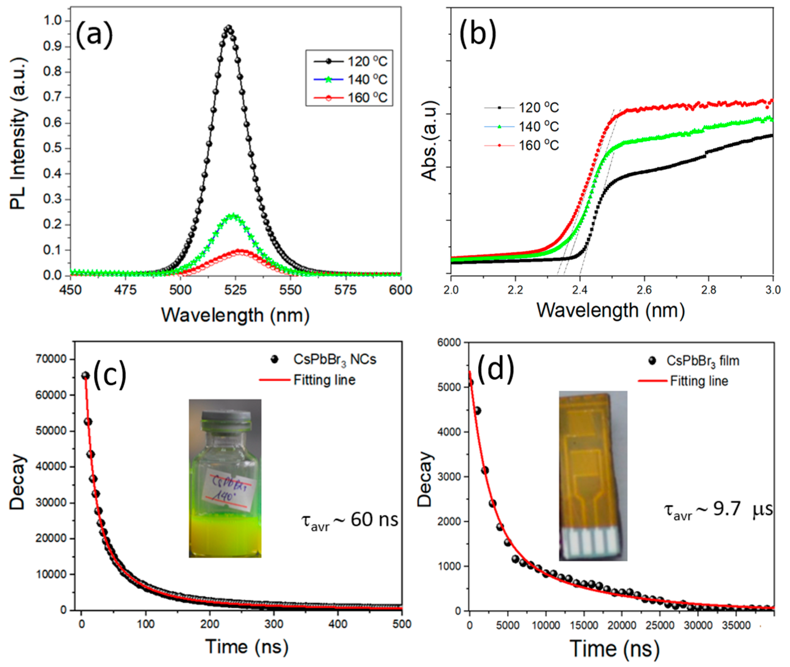
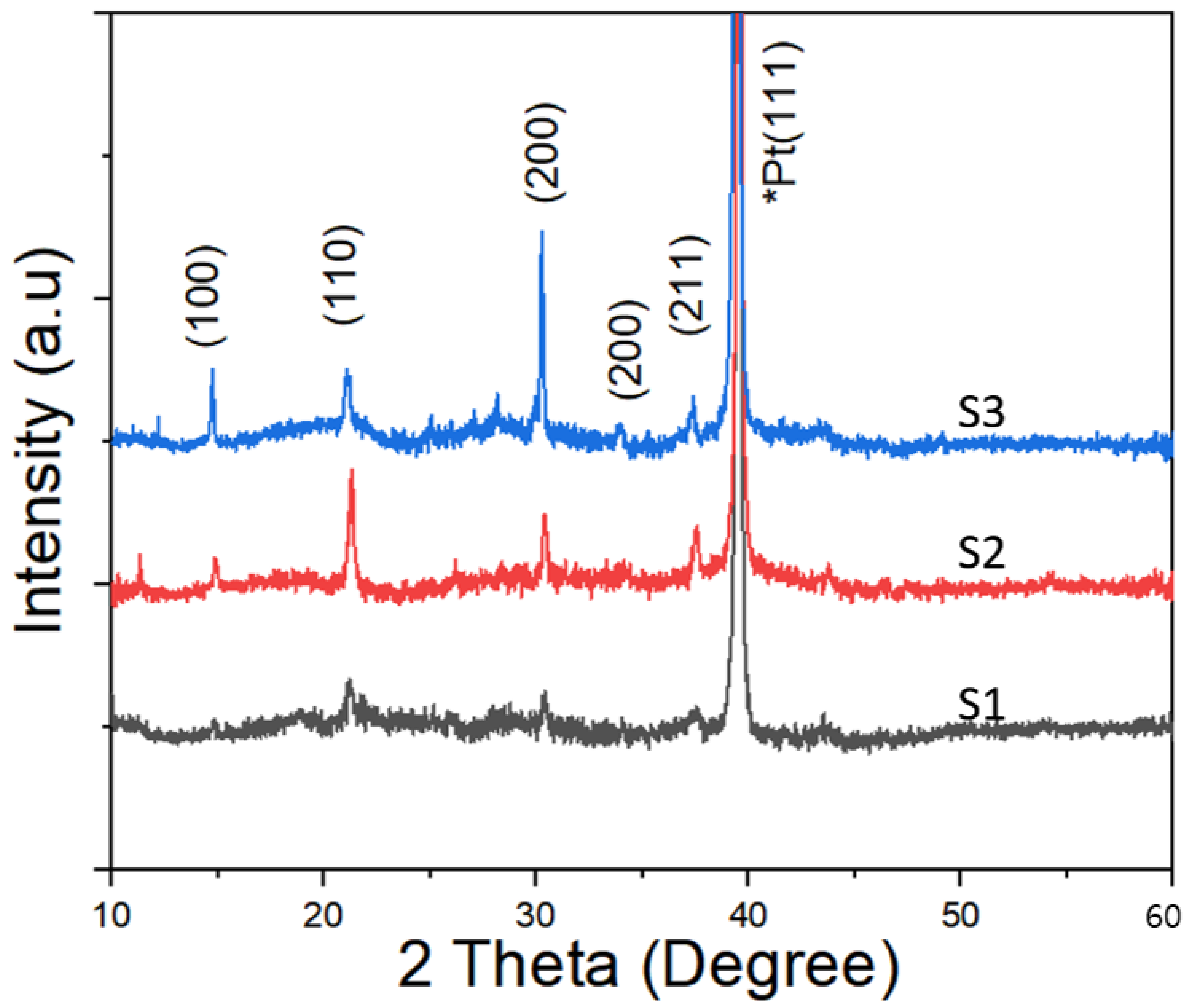
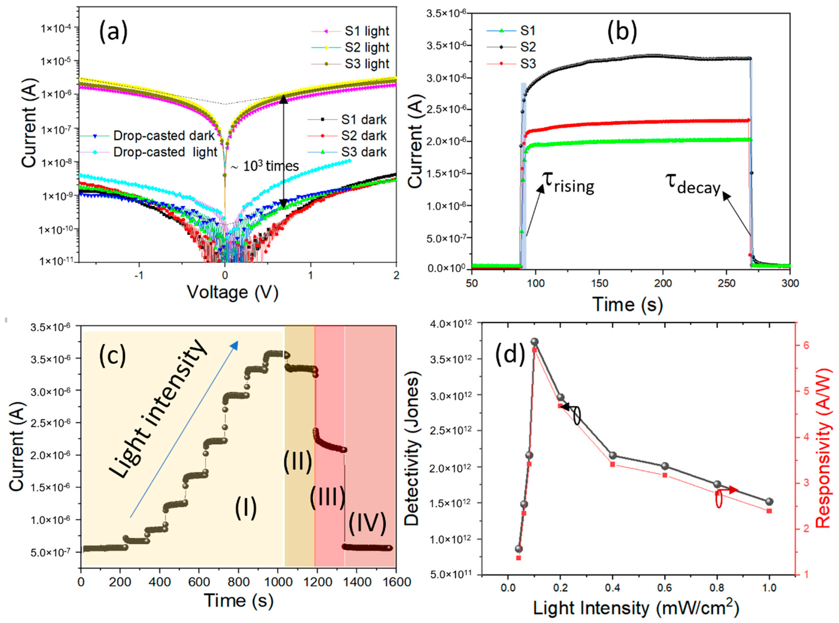
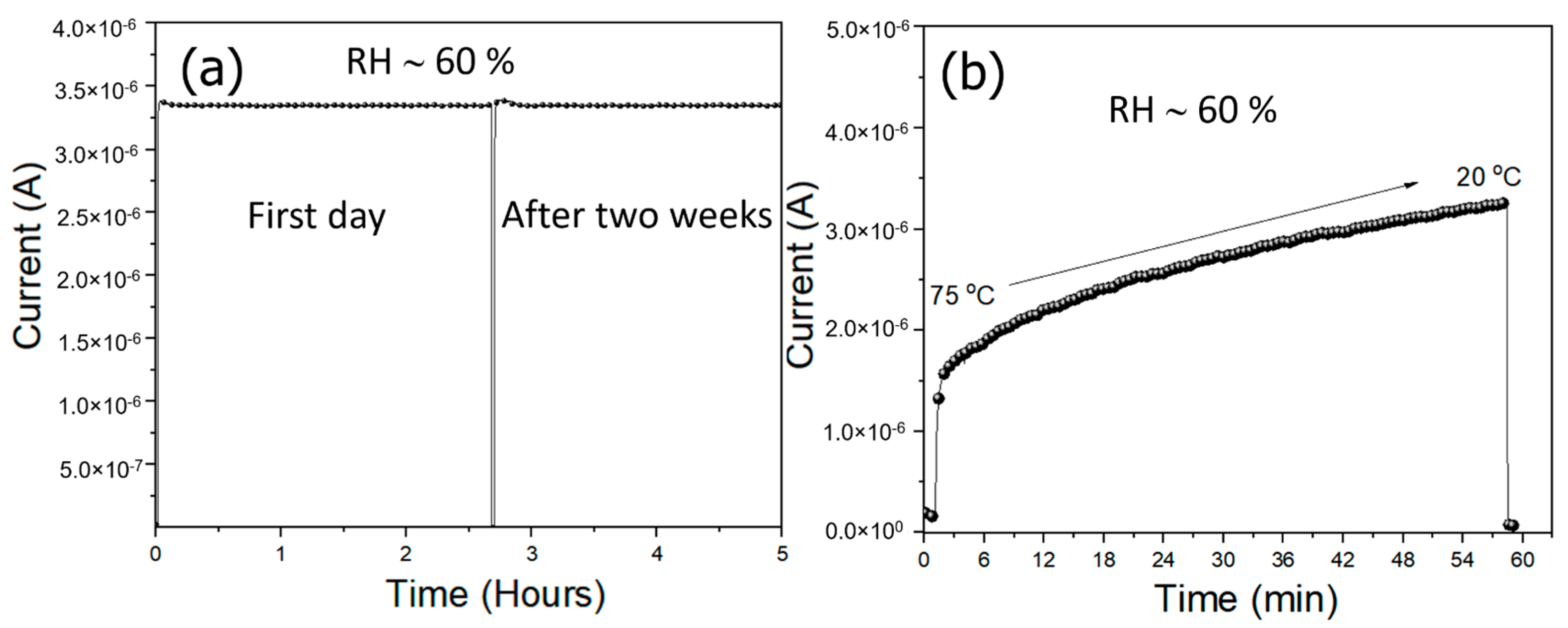
3. Results and Discussion

CsPbBr3 nanoparticles are synthesized using the hot-injection method which is similar to a previous method proposed by M. Kovalenco and colleagues [29]. It is well known that reaction temperature is the important parameter for controlling the size of nanoparticles. As shown in Figure 1, the size of nanoparticles stays in the range of 8 to 12 nm with reaction temperature of around 120 to 140 °C. By increasing the reaction temperature up to 160 °C, the particle size sharply increased up to 30–40 nm. Usually after fabrication, a purification procedure of the QD crude solution is required. Typically, a polar solvent such as ethyl acetate is used to promote the precipitation during centrifugal purification [30]. After that, the QD was redispersed in toluene nonpolar solvent for long-time storage. Moreover, the washing process can effectively remove excess ligands of CsPbBr3 QDs and enhance the opto-electronic performance. Here, we realized that by adding a small amount of toluene (T) nonpolar solvent into ethyl acetate (EA) polar solvent during the centrifugal process could control the precipitation process of CsPbBr3 NC film.
We first demonstrate the mixed EA/T solvent effect on the precipitation of the crude CsPbBr3 NC solution. A schematic illustration for fabrication of CsPbBr3 NC film via the centrifuge coating method is shown in Figure 2a. For this, a mixture of crude NC solution with various EA/T volume ratios was centrifuged at 15,000 rpm for 3 min. The photos, as shown in Figure 2b, indicated that the CsPbBr3 NCs in crude solution were formed a yellow-green film on the wall of the centrifugal tubes when centrifuged with the volume ratio of EA/T from 1:0 to 1:0.4. Without toluene addition, The NCs are agglomerated in non-uniform CsPbBr3 NC precipitation onto the wall of the tube. Conversely, with the excess of toluene content of 1:0.5 and 1:0.7, the particles can only settle at the bottom of the tube. As can be seen, the EA/T volume ratio of 1:0.2 shows a thick and uniform yellow film on the tube wall in comparison to the rest, suggesting that it was the optimal condition for the centrifugal coating film′s purpose. Then, by placing a Pt electrode surface so that it faces the centrifugal force in the tube, a green-yellow film was coated onto the electrode surface (see Figure 2b).
The surface and cross-section morphologies of the as-prepared CsPbBr3 films were obtained via scanning electron microscopy (SEM) as shown in Figure 3. Both surface and cross-section images showed a dense packaging as well as compact, crack-free CsPbBr3 films. The average particle sizes of 8, 12, and >30 nm for each sample are consistent with TEM images described above (Figure 3a,c,d), and an approximately 500 nm-thick film adhered directly to the SiO2 substrate (Figure 3b). For comparison, the SEM image of drop-coated film was measured and is shown in Figure 3e. It can be seen that the image shows nanoparticles assembled discretely when compared to the sample made by centrifugal coating method. It is worth noting that isolated ligand-coated nanoparticles usually prevent the film′s SEM image from achieving high magnification. In this work, all CsPbBr3 NCs prepared at 120 °C (S1), 140 °C (S2), and 160 °C (S3) with particle sizes ranging from 8 nm to >30 nm could be clearly seen in SEM images, implying that nanoparticles were not coated with organic long chain ligand; this allows us to hope that all films could have good opto-electrical properties for further application. The sample analyzed by EDX measurements showed a Cs:Pb:Br ratio of ~1:1:3 for CsPbBr3 NCs (Figure 3f).
The PL spectra of three CsPbBr3 NC coated films are shown in Figure 4a. The PL peaks are red-shifted from 515 nm to 526 nm, corresponding to a decrease in the bandgap energy from 2.4 to 2.35 eV for the CsPbBr3 NCs with various particle sizes from 8 to ~30 nm. The Tauc plot curves calculated from UV-Vis spectra of CsPbBr3 NCs solutions prepared at 120, 140, and 160 °C also confirm the change of the bandgap energy (Figure 4b).
Time-resolved photoluminescence (TRPL) was measured to clarify the change in the carrier charge transfer and recombination process for crude CsPbBr3 NCs and centrifugal coated film, as shown in Figure 4c,d. The three exponential decays are described in the following equation [31]:
I ( t ) = I 0 + A 1   exp ( t t 1 ) + A 2   exp ( t t 2 ) + A 3   exp ( t t 3 )
where I(t) is the luminescence intensity at time t; I0 is the luminescence intensity at time t = 0; t 1 ,   t 2 , and t 3 are short and long decay components, respectively; and A1, A2, and A3 are their pre-exponential factors, respectively. The average lifetimes (s) were evaluated using the following equation:
t avg = ( A 1 t 1 2 + A 2 t 2 2 + A 3 t 3 2 ) / ( A 1 t 1 + A 2 t 2 + A 3 t 3 )
As expected, the decay time was increased from 60 ns (crude NCs) to 9.7 ms (dense film). It could be said that the NCs that formed a dense film with carrier charge transfer within the film are larger than isolated crude NCs, causing the recombination probability of the electron-hole declines. This is an advantage for opto-electric applications such as solar cell or photodetector. The qualifications of CsPbBr3 NC centrifuge coated films were also confirmed by XRD analyses (Figure 5). All three samples exhibited a pure cubic phase (PDF# 54-0752), confirming the integrity of the perovskite structure.
The performances of three photodetector devices were under tungsten-halogen light source and are presented in Figure 6. Figure 6a shows the current–voltage (I–V) logarithm curves of devices with different particle size films. It can be observed that both the dark current and photocurrent (Plight = 1 mWcm−2) of the I–V curves are symmetrical under bias voltage applied from −2 V to +2 V with a gap of ~103 times for all three samples. The response/recovery behavior in a single on/off cycle for three samples is presented in Figure 6b. The corresponding photocurrents at a constant applied voltage were 1.9 × 10⁻⁶ (A), 3.4 × 10⁻⁶ (A), and 2.3 × 10⁻⁶ (A) for S1, S2, and S3 samples, respectively. Even so, the difference is negligible compared to the gap of 103 times between dark current and photocurrent. For comparison, the gap between the dark current and the photocurrent of the drop-coated film device is ~10 (from 2 × 10⁻⁹ to 1.2 × 10⁻⁸ A, see Figure 6a).
Photoresponse features have been plotted to infer the rise time (τr: Time taken for the photocurrent to rise from 10 to 90% of its amplitude) and decay time (τf: Time taken for the photocurrent to drop from 90 to 10% of its amplitude). The rise and decay times of devices were evaluated at about 4 s and 1 s for all three samples. Normally, the speed of response results involved using a light chopper. Because of limitations of the apparatus employed to acquire the photocurrent during the transient measurements, the rise and fall times should not be regarded as the absolute speed of response of our photodetectors. In fact, the actual photodetector response times are expected on the scale of the carrier lifetimes of the CsPbBr3 NC film, which is described in Figure 4c.
A detailed study of the as-prepared photodetector was performed by assessing their photocurrent as a function of light intensity and with different wavelength cutoff filters (for the S2 sample only). As shown in Figure 6c,d, the photocurrent values were effectively changed. As expected, the photocurrent increased with the increasing of illumination intensity (see the (I) zone in Figure 6c) from 0 to 1 mW/cm−2. Moreover, the photocurrent decreased with different wavelength cutoff filters (see (II)–(IV) zones in Figure 6c) and almost disappeared with 540 nm cutoff filter (IV) corresponding to the energy value of 2.3 eV (smaller than CsPbBr3 NCs bandgap of ~2.35 eV).
Two important parameters of the device, the sensitivity (R) and detection index (D*), can be obtained from Equation (3):
R = Iph/Plight
where Iph is the photocurrent, Plight is the light power intensity (1 mWcm−2). D = R/ 2 qI dark , where I dark is the dark current, q is the elementary charge (Coulomb). The highest values achieved for responsivity and specific detectivity were 6 A/W, 3.7 × 10¹² Jones, respectively, when the devices were exposed to tungsten-halogen lamp illumination with an intensity at 0.1 mW cm−2. The analytical parameters of CsPbBr3-based photodetectors are summarized in Table 1. The superior performance obtained from photodetectors via centrifuge deposited perovskite NC films might be attributed to the high intrinsic quality of the perovskite films (high quality compact films and with no pinholes).
For practical application, operational stability in air ambient as well as a mild-high temperature (up to 75 °C) are evaluated. Figure 7a shows that the photocurrent has no change after two weeks stored in air atmosphere without encapsulation (RH ~ 60%). The effect of ambient temperature on the operation of the component is observed by directly putting the sample on a heater holder at 75 °C and cooling to a temperature of 20 °C for a period of one hour. The photocurrent change according to temperature is recorded and presented in Figure 7b. As shown in the figure, the photocurrent started at ~50% value at 75 °C and increased with the decrease of ambient temperature; the photocurrents almost recovered to their original value. Thus, our photodetectors exhibited considerable moisture stability and mild temperature with no encapsulation for more than two weeks. The highly photodetector performance described in this work is expected to encourage the further development of all-inorganic perovskite nanocrystals films for optoelectronics applications.

4. Conclusions

We successfully fabricated CsPbBr3 NC film on a pre-patterned Pt/SiO2/Si substrate as a planar photodetector with metal/semiconductor/metal structure via a centrifuge coating method. A ~500 nm dense, pinhole- and crack-free CsPbBr3 NC film coating was achieved using a mixed toluene/ethyl acetate solvent. As a consequence, the photodetector device performance showed several figures of merit such as an on/off ratio of 103 times, responsivity of 6 A.W−1, and detectivity of 3.5 × 10¹² Jones (by using 0.1 mWcm2 tungsten-halogen light source). In comparison, the on/off ratio of the device fabricated by the centrifuge coating method was 102 times higher than by the drop-coating method. The results suggest that this is a potential method for fabricating high quality all-inorganic perovskite films for opto-electronic thin film devices such as photodetectors, LEDs, and solar cells.

Author Contributions

P.-N.T.: Methodology, original draft. B.-D.T.: Original draft. D.-C.N.: Review and Editing. T.-L.N.: formal analysis. V.-D.T.: formal analysis; T.-T.D.: Conceptualization. All authors have read and agreed to the published version of the manuscript.

Funding

This work was supported by the Vietnam Ministry of Education and Training (MOET) through research project Grant Number B2020_BKA_25_CTVL.

Institutional Review Board Statement

Not applicable.

Informed Consent Statement

Not applicable.

Data Availability Statement

Not applicable.

Conflicts of Interest

The authors declare no conflict of interest.

References

  1. Ji, K.; Yuan, J.; Li, F.; Shi, Y.; Ling, X.; Zhang, X.; Zhang, Y.; Lu, H.; Yuan, J.; Ma, W. High-efficiency perovskite quantum dot solar cells benefiting from a conjugated polymer-quantum dot bulk heterojunction connecting layer. J. Mater. Chem. A 2020, 8, 8104–8112. [Google Scholar] [CrossRef]
  2. Wang, H.; Zhang, X.; Wu, Q.; Cao, F.; Yang, D.; Shang, Y.; Ning, Z.; Zhang, W.; Zheng, W.; Yan, Y.; et al. Trifluoroacetate induced small-grained CsPbBr3 perovskite films result in efficient and stable light-emitting devices. Nat. Commun. 2019, 10, 665. [Google Scholar] [CrossRef] [PubMed] [Green Version]
  3. Liu, H.; Zhang, X.; Zhang, L.; Yin, Z.; Wang, D.; Meng, J.; Jiang, Q.; Wang, Y.; You, J. A high-performance photodetector based on an inorganic perovskite–ZnO heter-ostructure. J. Mater. Chem. C 2017, 5, 6115–6122. [Google Scholar] [CrossRef]
  4. Saeed, M.A.; Kim, S.H.; Kim, H.; Liang, J.; Woo, H.Y.; Kim, T.G.; Yan, H.; Shim, J.W. Indoor Organic Photovoltaics: Optimal Cell Design Principles with Synergistic Parasitic Resistance and Optical Modulation Effect. Adv. Energy Mater. 2021, 11, 2003103. [Google Scholar] [CrossRef]
  5. Saeed, M.A.; Cheng, S.; Biswas, S.; Kim, S.H.; Kwon, S.-K.; Kim, H.; Kim, Y.-H.; Shim, J.W. Remarkably high performance of organic photovoltaic devices with 3,9-bis(2-methylene- (3-(1,1-dicyanomethylene)-indanone))-5,5,11,11-tetrakis(4-hexyl meta-phenyl)-dithieno[2,3-d:2′,3′-d′]-s-indaceno[1,2-b:5,6-b′]dithiophene)-ethylhexyloxy] photoactive acceptor under halogen light illumination. J. Power Sources 2021, 518, 230782. [Google Scholar] [CrossRef]
  6. Saeed, M.A.; Yoo, K.; Kang, H.C.; Shim, J.W.; Lee, J.-J. Recent developments in dye-sensitized photovoltaic cells under ambient illumination. Dye. Pigment. 2021, 194, 109626. [Google Scholar] [CrossRef]
  7. Wu, T.; Qin, Z.; Wang, Y.; Wu, Y.; Chen, W.; Zhang, S.; Cai, M.; Dai, S.; Zhang, J.; Liu, J.; et al. The Main Progress of Perovskite Solar Cells in 2020–2021. Nano-Micro Lett. 2021, 13, 152. [Google Scholar] [CrossRef]
  8. Zhang, H.; Fu, X.; Tang, Y.; Wang, H.; Zhang, X.; Yu, W.; Wang, X.; Zhang, Y.; Xiao, M. Phase segregation due to ion migration in all-inorganic mixed-halide perovskite nanocrystals. Nat Commun. 2019, 10, 1088. [Google Scholar] [CrossRef] [Green Version]
  9. Wang, Y.; Quintana, X.; Kim, J.; Guan, X.; Hu, L.; Lin, C.-H.; Jones, B.T.; Chen, W.; Wen, X.; Gao, H.; et al. Phase segregation in inorganic mixed-halide perovskites: From phenomena to mechanisms. Photon-Res. 2020, 8, A56–A71. [Google Scholar] [CrossRef]
  10. Li, X.; Wu, Y.; Zhang, S.; Cai, B.; Gu, Y.; Song, J.; Zeng, H. CsPbX3 Quantum Dots for Lighting and Displays: Room Tempera-ture Synthesis, Photoluminescence Superiorities, Underlying Origins and White Light-Emitting Diodes. Adv. Funct. Mater. 2016, 26, 2435–2445. [Google Scholar] [CrossRef]
  11. Suh, Y.H.; Kim, T.; Choi, J.W.; Lee, C.L.; Park, J. High-Performance CsPbX3 Perovskite Quantum-Dot Light-Emitting Devices via Solid-State Ligand Exchange. ACS Appl. Nano Mater. 2018, 1, 488–496. [Google Scholar] [CrossRef]
  12. Chaudhary, B.; Kshetri, Y.K.; Kim, H.-S.; Lee, S.W.; Kim, T.-H. Current status on synthesis, properties and applications of CsPbX3 (X = Cl, Br, I) perovskite quantum dots/nanocrystals. Nanotechnology 2021, 32, 502007. [Google Scholar] [CrossRef] [PubMed]
  13. Swarnkar, A.; Marshall, A.R.; Sanehira, E.M.; Chernomordik, B.D.; Moore, D.T.; Christians, J.A.; Chakrabarti, T.; Luther, J.M. Quantum dot-induced phase stabilization of α-CsPbI3 perovskite for high-efficiency photovoltaics. Science 2016, 354, 92–95. [Google Scholar] [CrossRef] [PubMed] [Green Version]
  14. Hao, M.; Bai, Y.; Zeiske, S.; Ren, L.; Liu, J.; Yuan, Y.; Zarrabi, N.; Cheng, N.; Ghasemi, M.; Chen, P.; et al. Ligand-assisted cation-exchange engineering for high-efficiency colloidal Cs1−xFAxPbI3 quantum dot solar cells with reduced phase segregation. Nat. Energy 2020, 5, 79–88. [Google Scholar] [CrossRef]
  15. Kim, G.; Min, H.; Lee, K.S.; Lee, D.Y.; Yoon, S.M.; Seok, S.I. Impact of strain relaxation on performance of α-formamidinium lead iodide perovskite solar cells. Science 2020, 370, 108–112. [Google Scholar] [CrossRef]
  16. Wang, C.; Chesman, A.S.R.; Yin, W.; Frazer, L.; Funston, A.M.; Jasieniak, J.J. Facile purification of CsPbX3 (X = Cl, Br, I) perovskite nanocrystals. J. Chem. Phys. 2019, 151, 121105. [Google Scholar] [CrossRef]
  17. Yang, T.; Zhang, Z.; Ding, Y.; Yin, N.; Liu, X. Nondestructive purification process for inorganic perovskite quantum dot solar cells. J. Nanoparticle Res. 2019, 21, 101. [Google Scholar] [CrossRef]
  18. Zhao, Q.; Hazarika, A.; Chen, X.; Harvey, S.P.; Larson, B.W.; Teeter, G.R.; Liu, J.; Song, T.; Xiao, C.; Shaw, L.; et al. High efficiency perovskite quantum dot solar cells with charge separating hetero-structure. Nat. Commun. 2019, 10, 2842. [Google Scholar] [CrossRef]
  19. Yang, Z.; Wang, M.; Li, J.; Dou, J.; Qiu, H.; Shao, J. Spray-Coated CsPbBr3 Quantum Dot Films for Perovskite Photodiodes. ACS Appl. Mater. Interfaces 2018, 10, 26387–26395. [Google Scholar] [CrossRef]
  20. Hamukwaya, S.; Hao, H.; Zhao, Z.; Dong, J.; Zhong, T.; Xing, J.; Hao, L.; Mashingaidze, M. A Review of Recent Developments in Preparation Methods for Large-Area Perovskite Solar Cells. Coatings 2022, 12, 252. [Google Scholar] [CrossRef]
  21. Fan, T.; Lü, J.; Chen, Y.; Yuan, W.; Huang, Y. Random lasing in cesium lead bromine perovskite quantum dots film. J. Mater. Sci. Mater. Electron. 2018, 30, 1084–1088. [Google Scholar] [CrossRef]
  22. Algadi, H.; Mahata, C.; Woo, J.; Lee, M.; Kim, M.; Lee, T. Enhanced Photoresponsivity of All-Inorganic (CsPbBr3) Perovskite Nanosheets Photodetector with Carbon Nanodots (CDs). Electronics 2019, 8, 678. [Google Scholar] [CrossRef] [Green Version]
  23. Zhou, L.; Yu, K.; Yang, F.; Zheng, J.; Zuo, Y.; Li, C.; Cheng, B.; Wang, Q. All-inorganic perovskite quantum dot/mesoporous TiO2 composite-based photodetectors with enhanced performance. Dalton Trans. 2017, 46, 1766–1769. [Google Scholar] [CrossRef] [PubMed]
  24. Dong, Y.; Gu, Y.; Zou, Y.; Song, J.; Xu, L.; Li, J.; Xue, J.; Li, X.; Zeng, H. Improving All-Inorganic Perovskite Photodetectors by Preferred Orientation and Plasmonic Effect. Small 2016, 12, 5622–5632. [Google Scholar] [CrossRef] [PubMed]
  25. Yan, S.; Li, Q.; Zhang, X.; Tang, S.; Lei, W.; Chen, J. A vertical structure photodetector based on all-inorganic perovskite quantum dots. J. Soc. Inf. Disp. 2020, 28, 9–15. [Google Scholar] [CrossRef]
  26. Shin, H.; Oytun, F.; Kim, J.; Lee, B.; Kim, J.; Basarir, F.; Choi, H. Cost-effective centrifuge coating method for silver nanowire-based transparent conducting electrode. Electrochim. Acta 2020, 337, 135839. [Google Scholar] [CrossRef]
  27. Huang, Y.Y.S.; Terentjev, E.M. Transparent nanostructured electrode by centrifuge coating. In Proceedings of the 2012 12th IEEE International Conference on Nanotechnology (IEEE-NANO), Birmingham, UK, 20–23 August 2012; pp. 1–4. [Google Scholar]
  28. Kim, Y.; Yassitepe, E.; Voznyy, O.; Comin, R.; Walters, G.; Gong, X.; Kanjanaboos, P.; Nogueira, A.F.; Sargent, E.H. Efficient Luminescence from Perovskite Quantum Dot Solids. ACS Appl. Mater. Interfaces 2015, 7, 25007–25013. [Google Scholar] [CrossRef]
  29. Protesescu, L.; Yakunin, S.; Bodnarchuk, M.; Krieg, F.; Caputo, R.; Hendon, C.; Yang, R.; Walsh, A.; Kovalenko, M. Nano-crystals of Cesium Lead Halide Perovskites (CsPbX3, X = Cl, Br, and I): Novel Optoelectronic Materials Showing Bright Emission with Wide Color Gamut. Nano Lett. 2015, 15, 3692–3696. [Google Scholar] [CrossRef] [Green Version]
  30. Chen, L.-C.; Tien, C.-H.; Tseng, P.-W.; Tseng, Z.-L.; Huang, W.-L.; Xu, Y.-X.; Kuo, H.-C. Effect of Washing Solvents on the Properties of Air-Synthesized Perovskite CsPbBr3 Quantum Dots for Quantum Dot-Based Light-Emitting Devices. IEEE Access 2020, 8, 159415–159423. [Google Scholar] [CrossRef]
  31. Nguyen, T.T.T.; Luu, T.N.; Nguyen, D.H.; Duong, T.T. Comparative Study on Backlighting Unit Using CsPbBr3 Nanocrystals/KSFM Phosphor + Blue LED and Commercial WLED in Liquid Crystal Display. J. Electron. Mater. 2021, 50, 1827–1834. [Google Scholar] [CrossRef]
  32. Li, X.; Yu, D.; Cao, F.; Gu, Y.; Wei, Y.; Wu, Y.; Song, J.; Zeng, H. Healing All-Inorganic Perovskite Films via Recyclable Dissolution-Recyrstallization for Compact and Smooth Carrier Channels of Optoelectronic Devices with High Stability. Adv. Funct. Mater. 2016, 26, 5903–5912. [Google Scholar] [CrossRef]
  33. Song, J.; Xu, L.; Li, J.; Xue, J.; Dong, Y.; Li, X.; Zeng, H. Monolayer and Few-Layer All-Inorganic Perovskites as a New Family of Two-Dimensional Semiconductors for Printable Optoelectronic Devices. Adv. Mater. 2016, 28, 4861–4869. [Google Scholar] [CrossRef] [PubMed]
  34. Ding, J.; Du, S.; Zuo, Z.; Zhao, Y.; Cui, H.; Zhan, X. High Detectivity and Rapid Response in Perovskite CsPbBr3 Single-Crystal Photodetector. J. Phys. Chem. C 2017, 121, 4917–4923. [Google Scholar] [CrossRef]
Figure 1. TEM images and corresponding particle size distribution of CsPbBr3 NCs prepared at 120 °C (a,b), 140 °C (c,d), and 160 °C (e,f). The photos of crude CsPbBr3 solution are shown in insets of figures.
Crystals 12 00587 g001
Figure 2. (a) Schematic illustration for fabrication of CsPbBr3 NC film via the centrifuge coating method, (b) photos of CsPbBr3 film coated onto centrifuge tubes and pre-patterned Pt electrode/SiO2/Si substrates with various toluene/ethyl acetate solvent volume ratios. Each vial was centrifuged at 15,000 rpm for 3 min.
Crystals 12 00587 g002
Figure 3. (a,c,d) SEM images of centrifuge coating films from different crystal sizes of CsPbBr3 NCs. (b) Cross-section image of 8 nm-particles size CsPbBr3 NC films. (e) SEM image of CsPbBr3 NC films by drop-cast film. (f) EDX spectrum of CsPbBr3 NC films.
Crystals 12 00587 g003
Figure 4. (a) PL spectra of CsPbBr3 films prepared at various temperatures; (b) The Tauc plot curve CsPbBr3 NCs solutions prepared at 120, 140, and 160 °C. (c,d) Decay curves of crude CsPbBr3 NCs and cetrifuge coated CsPbBr3 film.
Crystals 12 00587 g004
Figure 5. XRD patterns of CsPbBr3 NC films coated on pre-patterned Pt electrodes.
Crystals 12 00587 g005
Figure 6. (a) Logarithmic I–V curves of photodetectors in the dark and under irradiation, (b) The response and recovery time analysis of the photodetectors. (c) Photocurrent versus various illumination intensities and different wavelength cutoff filters (380, 480, and 540 nm) of the S2 device. (d) Detectivity and responsivity vs. light intensity of the photodetector.
Crystals 12 00587 g006
Figure 7. (a) Photo current vs. ambient temperature, (b) Operational long-time photostability of non-encapsulated photodetector in air.
Crystals 12 00587 g007
Table 1. Comparison of device performance of CsPbBr3-based photodetectors.
Active
Materials
Wavelength
(nm)
Responsivity
(A/W)
Rise/Fall
(s)
On/Off RatioDetectivity
(Jones)
Ref
CsPbBr3 QDs 0.40 mWcm−2 @ 532 nm 4.7 × 10−30.2/1.31.6 × 10516.84 × 108[24]
CsPbBr3 micro-particles 1.01 mWcm−2 @ 442 nm 0.181.8/18 × 1036.1 × 1010[32]
CsPbBr3 nanosheets 0.35 mWcm−2 @ 442 nm 0.250.019/0.025 103-[33]
Single crystal CsPbBr31 mW @ 450 nm 0.028 90.7/57 1021.8 × 1011[34]
CsPbBr3 nano crystals film Halogen lamp
0.1 mW/cm2
6.04/1 1033.6 × 1012this work
Publisher’s Note: MDPI stays neutral with regard to jurisdictional claims in published maps and institutional affiliations.

