Article

Effect of Carrier Gas Flow Rate on the Morphology and Luminescence Properties of CsPbBr3 Microcrystals

National Synchrotron Radiation Laboratory, School of Nuclear Science and Technology, University of Science and Technology of China, Hefei 230029, China
*
Author to whom correspondence should be addressed.
Crystals 2022, 12(4), 479; https://doi.org/10.3390/cryst12040479
Submission received: 6 March 2022 / Revised: 20 March 2022 / Accepted: 27 March 2022 / Published: 31 March 2022

Abstract

:
All-inorganic halide perovskites, especially lead perovskite microcrystals, have attracted more and more attention because of their excellent photoelectric properties and chemical stability. Herein, high quality CsPbBr3 microcrystals with three different stable morphologies, namely microplate, frustum of a square pyramid and pyramid, were synthesized by the chemical vapor deposition (CVD) method through altering the flow rate of a carrier gas and were comparatively studied in structure and optical property. The photoluminescence (PL) results showed that the CsPbBr3 microplate has the best luminescence property. The structural characterization results by scanning electron microscope (SEM), X-ray photoelectron spectroscopy (XPS), X-ray diffraction (XRD), X-ray rocking curves (XRC) and Raman revealed that the flow rate of the carrier gas could manipulate the morphology evolution of CsPbBr3 microcrystals and further impact their luminescence properties.

1. Introduction

Lead halide perovskite (LHP) APbX3 (A = CH3NH3+, CH(NH2)2+, Cs+, X = Cl, Br, and I) materials have gained substantial attention over the past decades [1,2,3,4,5,6,7], owing to their excellent characteristics, including broadly tunable band gaps, high photoluminescence (PL) quantum efficiency, low nonradiative recombination rate, and direct band-gap [8,9,10,11]. For this reason, a large number of LHP-based photoelectric devices have been developed, including solar cells, low-threshold lasers, bright light-emitting diodes (LEDs) and photodetectors [12,13,14,15].
Among the various types of LHP-based devices, the ones based on organic–inorganic hybrid perovskites usually exhibit excellent performance because of the mutual modulation effects between organic and inorganic components. However, the issue of stability is a crucial factor for realizing the expected potential of such kind of solar cells [16]. Organic–inorganic hybrid perovskites are found to decompose easily in a humid environment on account of the existence of hygroscopic amine salt [17,18], and they show low thermal stability even in an inert atmosphere [19]. Comparatively, all-inorganic halide perovskite, which was first reported by Møller in 1958 [20], possesses a stronger tolerance for moisture, oxygen, heat, light, and electrical field. For example, Jin et al. reported an all-inorganic solar capacitor by integrating a perovskite solar cell unit and a supercapacitor unit into a single device that exhibits high open-circuit voltage and outstanding stability [21]. Xue et al. developed a self-powered, high-performance CsPbBr3 perovskite photodetector that shows the responsivity and detectivity of 0.3 A/W and 1.15 × 1013 cm∙Hz1/2/W, respectively, and has an anti-corrosion ability to water and alcohol [22]. Apart from outstanding stability, all-inorganic perovskites can also have a high light-harvesting capability [23] and display strong PL emission with narrow full width at half maximum (FWHM), with a PL quantum yield up to ~90% [24]. Besides, all-inorganic perovskites can also be doped by other elements and show more excellent properties. For example, Mn-doped CsPbCl3 nanocrystals (NCs) with high Mn substitution synthesized at room temperature showed excellent stability and luminescence property [25]. In addition, all-inorganic perovskites can be fabricated in heterojunction with other semiconductor materials to obtain more outstanding optoelectronic performance. For example, P.K. Giri et al. fabricated a vertical heterojunction photodetector with integrating CsPbBr3 nanocrystals on a large-area monolayer MoS2, and the photodetector showed a high responsivity (24.3 A W−1 at 405 nm) and extremely fast photo response with photocurrent growth and decay times of 5.5 and 24.0 μs, respectively [26]. Therefore, all-inorganic perovskites have been intensively investigated from the synthesis of crystals to optoelectronic properties. Compared with organic–inorganic hybrids perovskites, all-inorganic perovskites have many different morphologies, which are highly conducive for studying the principle of intrinsic properties. However, the electrical and optical properties of all-inorganic perovskites with different morphologies still have not been studied widely [27,28].
At present, wet chemistry, a common synthesis method, is widely used to synthesize all-inorganic perovskites. Although people could get high quality perovskites by using wet chemistry, it may introduce unnecessary impurities from solvents and surfactants. In contrast, all-inorganic perovskite crystals that were synthesized by chemical vapor deposition (CVD) have higher purity [29] and have no ligands or other impurities, which are beneficial for us to study the intrinsic properties of perovskites. Recent studies have found that the process parameters of CVD, such as temperature, pressure, growth time, etc., can sometimes significantly influence the morphology and further impact the property of the samples. The effect of the flow rate of a carrier gas, one of the key parameters in the CVD process, is intensively explored in the growth of crystals such as graphene and MoS2 [30,31]. However, there are still few reports about how the flow rate affects the growth of CsPbBr3.
Here, CsPbBr3 microcrystals with three different morphologies, namely microplate, frustum of a square pyramid and pyramid, were synthesized by adjusting the flow rate of the carrier gas in the CVD process. A scanning electron microscope (SEM) and atomic force microscope (AFM) were used to explore the morphology, while X-ray rocking curve (XRC), X-ray diffraction (XRD), X-ray photoelectron spectroscopy (XPS) and Raman were applied to investigate the structure of the CsPbBr3 microcrystals. The PL results revealed the luminescence properties of CsPbBr3 microcrystals. The diversity of morphologies of all-inorganic perovskite microcrystals were demonstrated, and the relationship between intrinsic structure and optical properties was explored. Our findings provided a new insight into the structure–function relationship of all-inorganic perovskites, which can be a valuable reference for design of outstanding photoelectric devices.

2. Materials and Methods

Materials: High-purity (>98%) PbBr2 powder was bought from Alfa Aesar. CsBr powder with a purity of 99.5%, acetone and ethanol were purchased from Sinopharm Chemical Reagent Co., Ltd. The silicon wafer (diameter: 100 mm, thickness: 525 μm) obtained from HeFei Crystal Technical Material Co., Ltd. (Hefei, China) was cleaved into 50 × 20 mm slices, which were used as the substrate.
Pretreatment of substrate: The silicon substrate was first washed ultrasonically at room temperature in acetone, ethanol and deionized water for 15 min separately to remove the organic contaminants on the surface, was then placed into the piranha solution at 90 °C for 2 h to dissolve the oxide overlayer, and lastly, was cleaned and dried by deionized water and ultrahigh purity N2.
Synthesis of CsPbBr3 perovskite microcrystals: The CsPbBr3 perovskite microcrystals were synthesized by a vapor-phase method using a home-built CVD system that was equipped with a tube furnace having two heating zones, as shown in Figure 1. The source materials were the mixed powder of PbBr2 (36.7 mg) and CsBr (42.6 mg) with a molar ratio of 1:2, and then they were placed into a quartz boat. Next, the quartz boat was placed into the center of heating zone I of the furnace. The silicon substrate was placed in the center of heating zone II with a distance of about 20 cm from the source materials. The quartz tube was first evacuated to a low vacuum state by a turbo molecular pump, and then it was filled with a high-purity Ar carrier gas with a flow rate of 40~120 sccm until the inner pressure reached 380 Torr. In the process of preparing the sample, zone I and zone II of the furnace were heated simultaneously to a temperature of 600 and 340 °C, respectively, which is the optimal condition to grow the target samples. The growth process lasted for 70 min at such a status and finished by stopping the heating of the furnace and allowing the system to cool down to room temperature naturally.
Characterization: The morphologies and elemental mapping information of the CsPbBr3 microcrystals were obtained using SEM (HITACHI, SU8220, Tokyo, Japan) and the accessory energy distribution spectroscopy (EDS) method. The AFM images of the CsPbBr3 microcrystals were obtained using the Atomic Force Microscope (Veeco, diInnova, New York, NY, USA).
The XPS tests were performed to obtain the oxidation states of the elements in the CsPbBr3 microcrystals. The XPS was conducted at room temperature using the spectrometer (Thermo Scientific Escalab 250, Westborough, MA, USA) equipped with an aluminum anode.
The phase and structure information of CsPbBr3 microcrystals was collected at room temperature by using the Rigaku TTR-III X-ray diffractometer equipped with Cu Kα radiation. The XRC were scanned using a high-resolution X-ray diffractometer (Malvern PANalytical, X’Pert3 MRD, Waltham, MA, USA) to investigate the quality of the CsPbBr3 microcrystals.
Time-resolved photoluminescence results were collected from a Lecroy (New York, NY, USA) Wave Runner 6100 Digital Oscilloscope (1 GHz) equipped with a tunable laser (pulse width = 4 ns, gate = 500 ns) as the excitation source.
The Raman results were obtained on the HORIBA (Jobin Yvon, Paris, French) LabRAM HR Evolution system using a 633 nm laser light at room temperature.
For the purpose of detecting the optical property of the CsPbBr3 microcrystals, the PL measurements were carried out at room temperature on the HORIBA LabRAM HR Evolution system by using an excitation laser with a wavelength of 325 nm at constant power mode.
The Raman and PL measurements were performed on a single microcrystal.

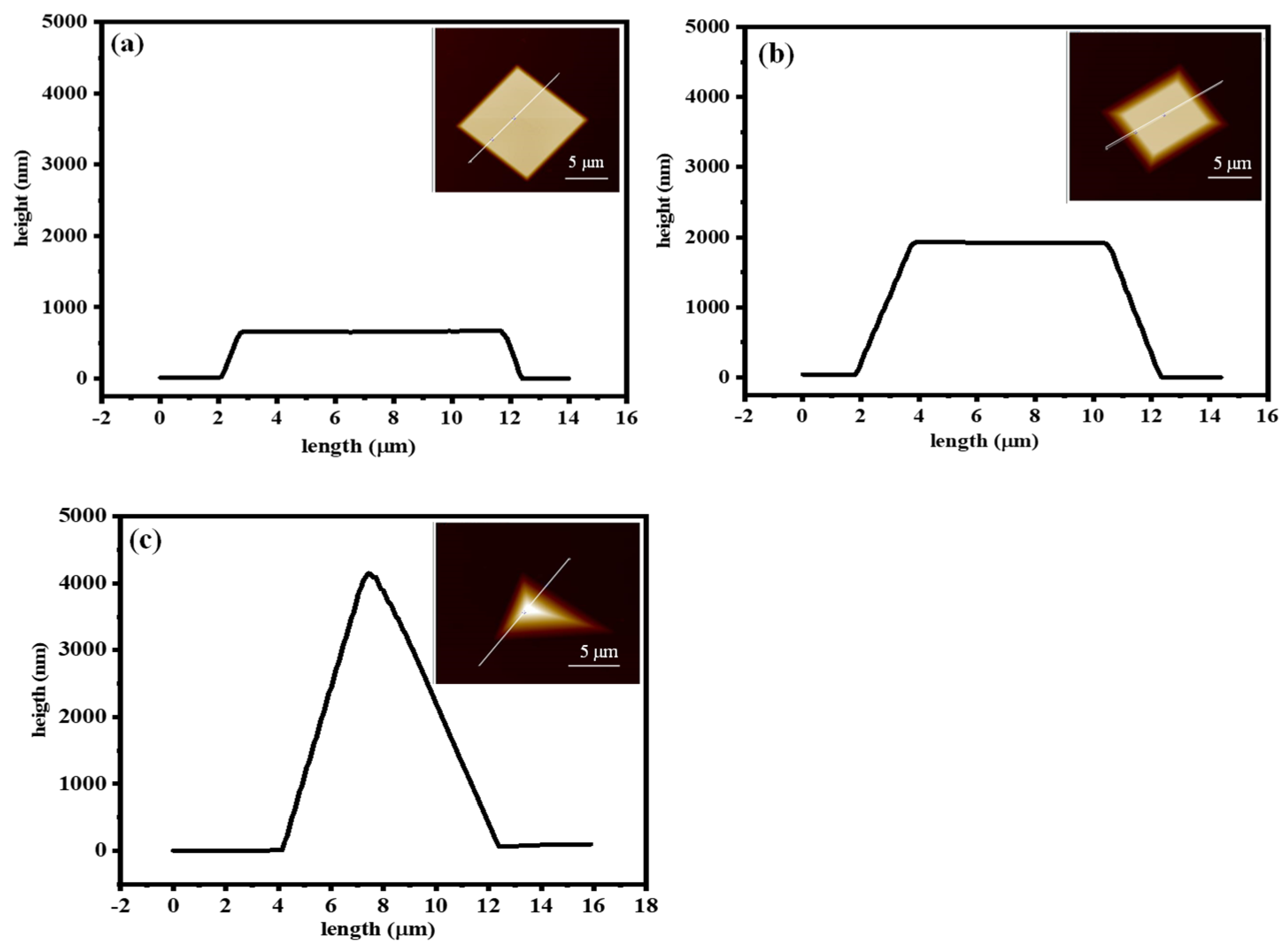
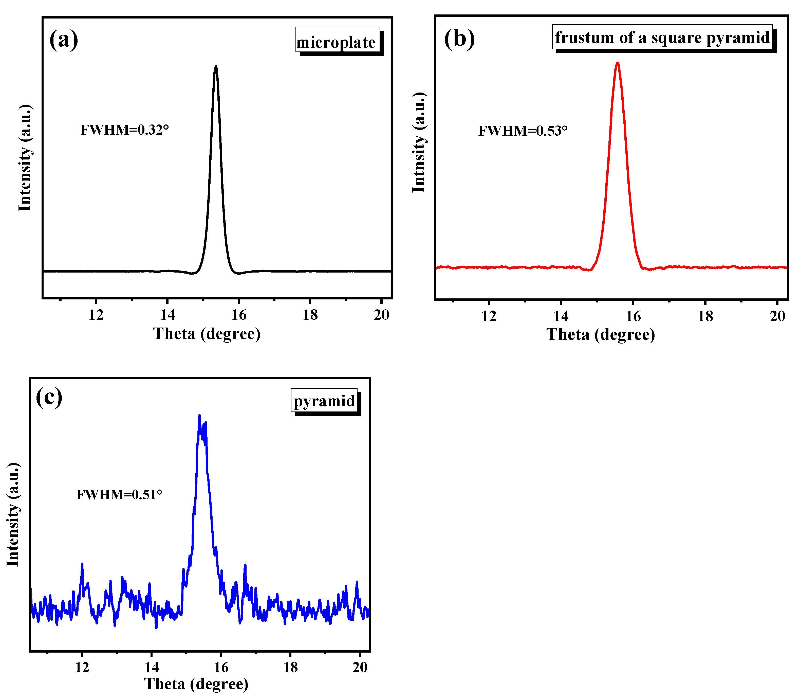
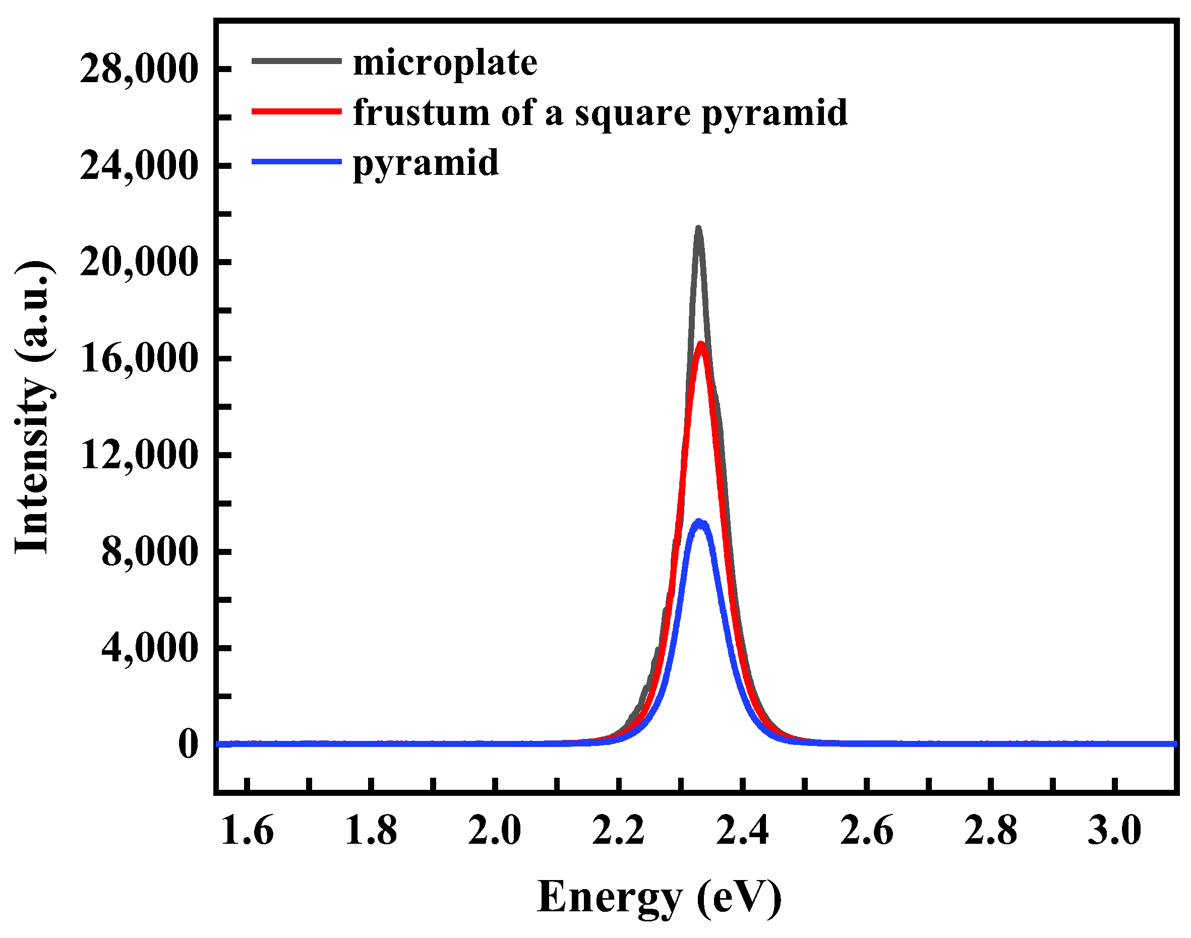
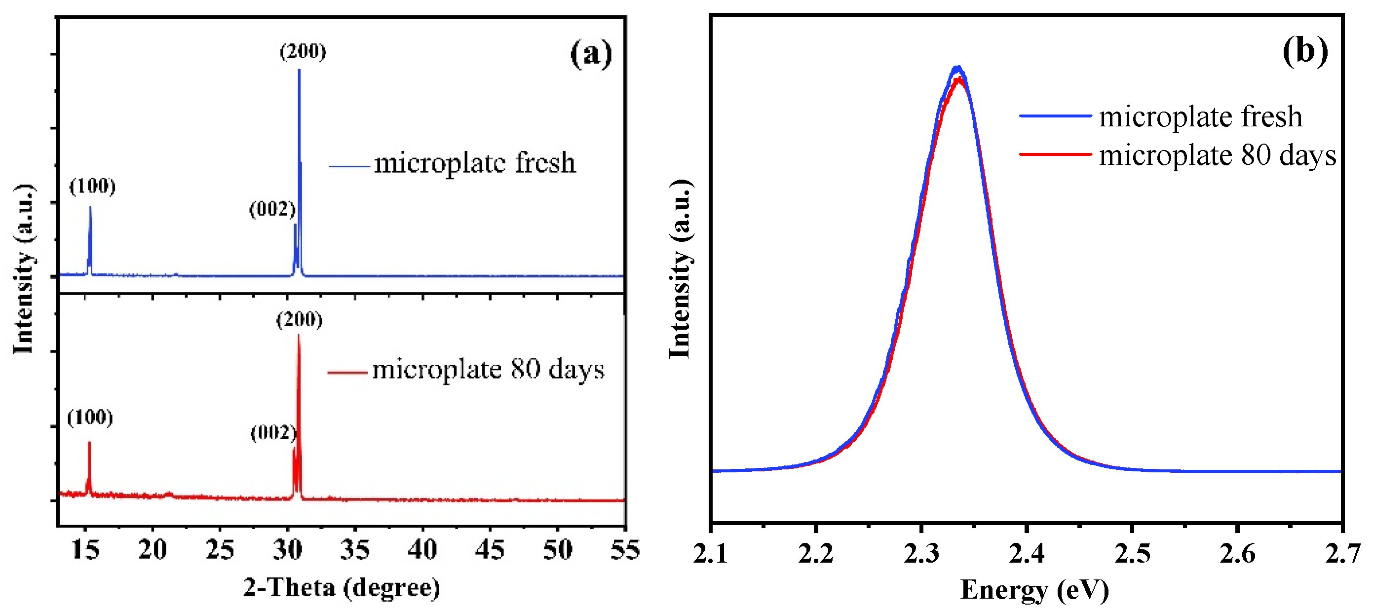
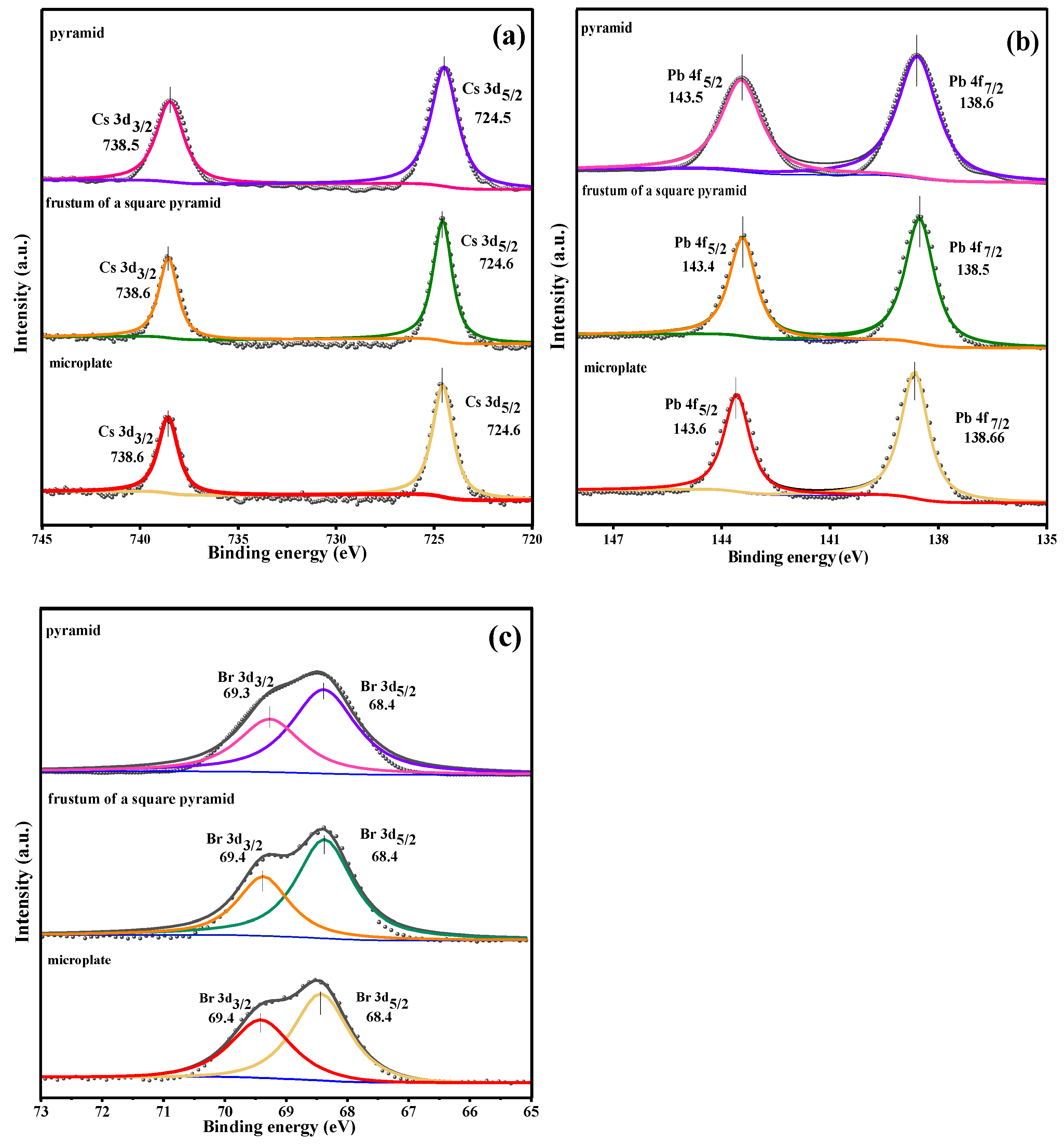
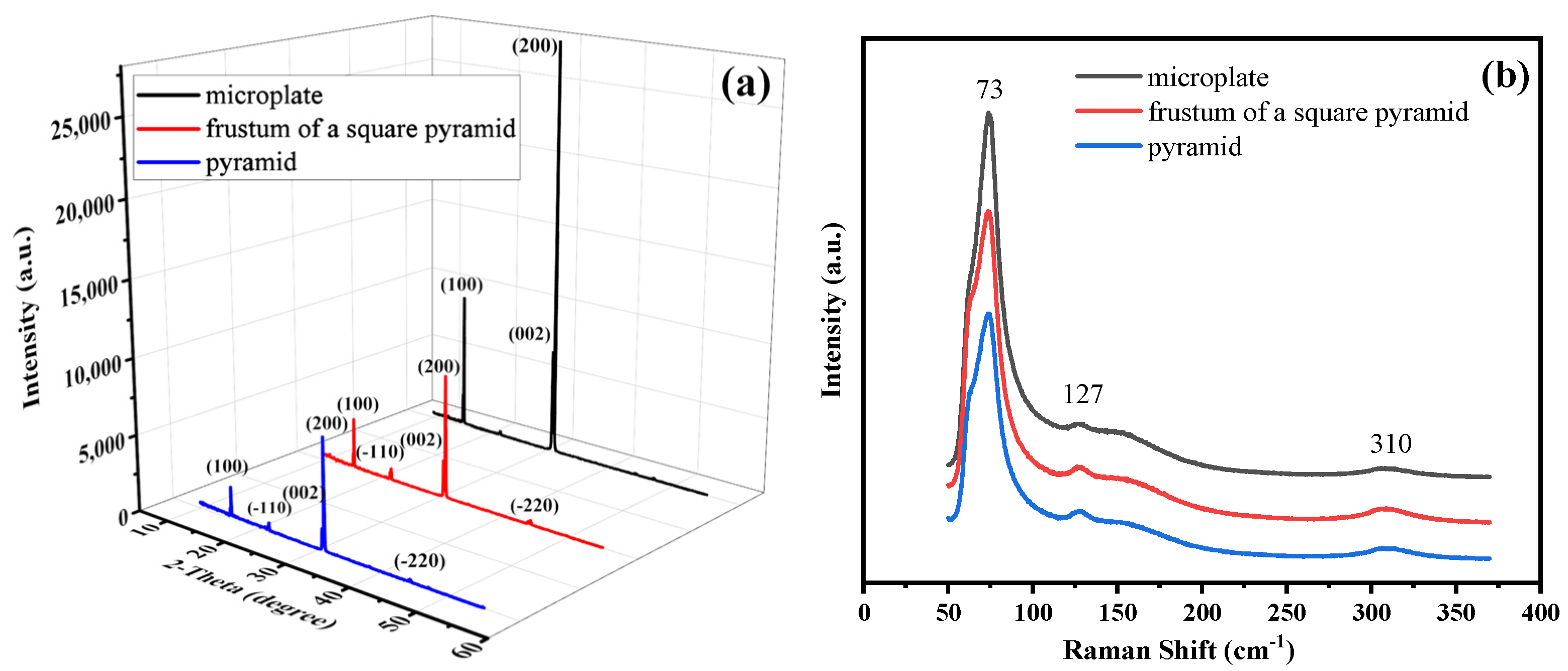
3. Results and Discussion

In the process of preparing CsPbBr3 perovskite materials using the CVD method, we found three typical microcrystals with the morphologies of a microplate, frustum of a square pyramid and pyramid, which could be repeatedly synthesized simply by controlling the flow rate of the carrier gas Ar when the other growth parameters are optimized and fixed. Figure 2a–c showed the SEM images of the samples on the silicon substrate obtained at a flow rate 40, 80 and 120 sccm, respectively. As we can see, the microcrystals in the form of the microplate, frustum of a square pyramid and pyramid dominated in number in each corresponding image. However, the densities of the pyramid and frustum of a square pyramid were higher than that of microplate. This phenomenon is not hard to understand since a higher flow rate of carrier gas leads to more nucleation, which would further evolve into higher crystallite density. The morphologies of the three kinds of microcrystals were verified by the AFM images and the scanned profile curves along the labeled lines in Figure 3a–c, respectively. All three microcrystals we selected have sharp edges: the square microplate in Figure 3a has a side length of about 10 μm and height of less than 1 μm, the frustum of a square pyramid in Figure 3b has an upper side length of about 7 μm, down side length of 10 μm and height of 2 μm, and the pyramid in Figure 3c has a width of about 8 μm and height of 4 μm. The AFM results indicate that the microplate tended to grow in two dimensions, while the frustum of a square pyramid and pyramid preferred to grow in three dimensions.
Then, the elemental composition and chemical stoichiometry of the microcrystals with different morphologies were analyzed by using energy dispersive spectroscopy (EDS), and the results are shown in Figure 4. As the elemental mappings in the illustration of Figure 4a–c demonstrate, all three kinds of microcrystals are composed of the elements Cs, Pb and Br, which are distributed uniformly and overlap perfectly in the microcrystals. Based on the weight percentages of the three elements shown in Figure 4, the atomic ratios of Cs: Pb: Br in the microplate, frustum of a square pyramid and pyramid are calculated to be 17.31:17.72:50.44, 17.16:17.76:50.56, and 16.17:17.19:53.69, respectively, which are all tightly close to the expected stoichiometric ratio of CsPbBr3 (1:1:3). Thus, it was necessary to determine the oxidation states of the three elements in the microcrystals by the technique XPS. Figure 5a–c demonstrates, respectively, the high-resolution core level XPS spectra of Cs, Pb and Br for the three kinds of microcrystals. From Figure 5, all the spin-orbit split doublets of Cs 3d, Pb 4f and Br 3d levels can be clearly observed, and the binding energies and spectral shapes reveal that the three elements are in the valence states of Cs+, Pb2+ and Br, respectively, which are well consistent with the previous report [32]. There were small differences in the binding energies of Cs 3d, Pb 4f, and Br 3d among these microcrystals with different morphologies, which means that the bonding structure of them are almost the same; the differences may come from the defects and the instrumental errors.
The above results indicate that the three kinds of microcrystals might be formed by the CsPbBr3 perovskites. Therefore, the XRD technique was applied to detect the crystal structures and phase information of the three microcrystals. The XRD pattern of the sample containing microplate, as displayed in Figure 6a, shows three strong and sharp diffraction peaks at 15.4°, 30.6° and 30.9°, which were indexed respectively to the (100), (002), (200) facets of the CsPbBr3 monoclinic phase [33]. While for the XRD spectra of the samples containing the frustum of a square pyramid and pyramid, besides the dominant peaks at 15.4°, 30.6° and 30.9°, two extra peaks at 21.7° and 44.2° became obvious, which can be indexed to the (-110) and (-220) facets of the monoclinic-phase CsPbBr3, respectively. This behavior indicates that there emerged a new orientation during the growth of the CsPbBr3 frustum of a square pyramid and pyramid. From the XRD patterns, we can conclude that the morphologies of the CsPbBr3 microcrystals are closely related to the flow rate of the carrier gas. At a low flow rate, the microplate grew slowly and orderly in two dimensions along the c-axis of the (100) direction, with the (100) plane as the terminal surface of the microcrystal, while the proportions of the side face for the frustum of a square pyramid and pyramid increased with the rise of the flow rate. This phenomenon may indicate that at a high flow rate, the mass transfer rate becomes faster, which means that the initial atoms may not have enough time to move into the right lattice location, where crystal domains can have the lowest surface free energy. Therefore, the subsequent atoms would grow in some specific direction in which the surface free energy of the crystal could decrease. As a consequence, CsPbBr3 microcrystals displayed different morphologies by altering the flow rate of the carrier gas. A similar growth mechanism has also been proposed by Ting Yu et al. in MoS2 crystal growth under different flow rates of carrier gas [34]. There were other little miscellaneous XRD peaks for the three CsPbBr3 microcrystals, which indicated that they all have the same pure phases and good crystalline quality. Apart from XRD, Raman spectra were also measured to study the structure of the CsPbBr3 microcrystals. The three spectra all showed well-resolved scattering bands at 73 cm−1, 127 cm−1 and 310 cm−1 assigned to the vibrational modes of [PbBr6]4−, the motion of Cs+ cations and the second-order phonon mode of octahedron, respectively, which exist typically in CsPbBr3 perovskites [35,36].
As a strong common method to determine the crystalline quality of the crystal [37], the XRC measurement was also carried out and the (200) facet’s rocking curves of CsPbBr3 microplate, frustum of a square pyramid and pyramid are shown in Figure 7. In general, a small FWHM represents good quality of crystal, low dislocation density and small residual stress in the crystal [38]. As Figure 7 shows, the FWHM of the CsPbBr3 microplate, frustum of a square pyramid and pyramid is 0.32°, 0.53°, 0.51°, respectively. The FWHM of each curve is small and close to each other. These results indicate that all of the CsPbBr3 microcrystals have good crystalline quality, which is consistent with the XRD result mentioned above.
For the CsPbBr3 microcrystals, their optical properties were of most concern; thus, PL measurements were performed to explore the optical characteristics of the three kinds of CsPbBr3 microcrystals. As shown in Figure 8, the PL emissions of the CsPbBr3 microplate, frustum of a square pyramid and pyramid are all located at around 2.3 eV, while the luminous intensities of them are obviously different. The PL intensity of the CsPbBr3 microplate is the strongest, which is 1.4 times that of the frustum of a square pyramid and 2.2 times that of the pyramid. This result indicated that the flow rate of the carrier gas could manipulate the morphology evolution of CsPbBr3 microcrystals and further impact their luminescence properties.
For the CsPbBr3 microplate with the strongest PL intensity, we further studied its long-term stability and time-resolved photoluminescence (TRPL). As shown in Figure 9a, the diffraction peaks of the microplate after 80 days of storage in ambient condition are still strong and sharp, which means that the microplate owns strong-phase stability. Figure 9b illustrates that the microplate has a good stability in optical properties, since the PL intensity of the microplate after 80 days of storage only has a small decrease compared with the fresh microplate. TRPL decay profiles of the microplate show that its average lifetime (τave) is about 117 ns (Figure 9c).

4. Conclusions

In summary, the microplate, frustum of a square pyramid and pyramid of CsPbBr3 microcrystals were synthesized by regulating the flow rate of a carrier gas in the CVD process. The XRD results indicated that the three CsPbBr3 microcrystals all have pretty good crystalline structure. The PL spectra showed that the CsPbBr3 microplate displayed the best luminescence property among them. This result indicated that the flow rate of the carrier gas could manipulate the morphology evolution of the CsPbBr3 microcrystals and further impact their luminescence properties. In addition, the CsPbBr3 microplate showed long-term stability and good lifetime performance. Our findings provided a meaningful reference for the design of outstanding photoelectric devices.

Author Contributions

Conceptualization, X.W.; methodology, X.W.; software, X.W., F.Y., J.H., Y.Y.; validation, F.X.; formal analysis, X.W.; investigation, X.W.; resources, F.X., X.W., F.Y., J.H., Y.Y.; data curation, X.W.; writing—original draft preparation, X.W.; writing—review and editing, X.W. and F.X.; visualization, X.W.; supervision, F.X.; project administration, F.X.; funding acquisition, F.X. All authors have read and agreed to the published version of the manuscript.

Funding

This research was funded by the National Natural Science Foundation of China (no. 11575187) and the National Key Research and Development Program (no. 2016YFB0700205).

Institutional Review Board Statement

Not applicable.

Informed Consent Statement

Not applicable.

Data Availability Statement

Not applicable.

Conflicts of Interest

The authors declare no conflict of interest.

References

  1. Zhao, Y.; Qiu, Y.; Feng, J.; Zhao, J.; Chen, G.; Gao, H.; Zhao, Y.; Jiang, L.; Wu, Y. Chiral 2D-Perovskite Nanowires for Stokes Photodetectors. J. Am. Chem. Soc. 2021, 143, 8437–8445. [Google Scholar] [CrossRef] [PubMed]
  2. Lu, C.H.; Biesold-Mcgee, G.V.; Liu, Y.; Kang, Z.; Lin, Z. Doping and ion substitution in colloidal metal halide perovskite nanocrystals. Chem. Soc. Rev. 2020, 49, 4953–5007. [Google Scholar] [CrossRef] [PubMed]
  3. Swarnkar, A.; Marshall, A.R.; Sanehira, E.M.; Chernomordik, B.D.; Moore, D.T.; Christians, A.J.; Luther, J.M. Tamoghna Chakrabarti. Quantum dot–induced phase stabilization of a-CsPbI3 perovskite for high-efficiency photovoltaics. Science 2016, 354, 92–96. [Google Scholar] [CrossRef] [PubMed] [Green Version]
  4. Shi, Z.; Li, Y.; Zhang, Y.; Chen, Y.; Li, X.; Wu, D.; Xu, T.; Shan, C.; Du, G. High-efficiency and air-stable perovskite quantum dots light-emitting diodes with an all-inorganic heterostructure. Nano Lett. 2017, 17, 313–321. [Google Scholar] [CrossRef] [PubMed]
  5. Li, X.; Bi, D.; Yi, C.; Décoppet, J.D.; Luo, J.; Zakeeruddin, S.M.; Hagfeldt, A.; Grätzel, M. A vacuum flash-assisted solution process for high-efficiency large-area perovskite solar cells. Science 2016, 353, 58–62. [Google Scholar] [CrossRef] [PubMed]
  6. Zhou, H.; Chen, Q.; Li, G.; Luo, S.; Song, T.B.; Duan, H.-S.; Hong, Z.; You, J.; Liu, Y.; Yang, Y. Interface engineering of highly efficient perovskite solar cells. Science 2014, 345, 542–546. [Google Scholar] [CrossRef]
  7. Liao, L.; Quan, K.; Bin, X.; Zeng, R.; Lin, T. Bandgap and Carrier Dynamic Controls in CsPbBr3 Nanocrystals Encapsulated in Polydimethylsiloxane. Crystals 2021, 11, 1132. [Google Scholar] [CrossRef]
  8. Zhang, Q.; Yin, Y. All-Inorganic Metal Halide Perovskite Nanocrystals: Opportunities and Challenges. ACS Cent. Sci. 2018, 4, 668–679. [Google Scholar] [CrossRef]
  9. Stranks, S.D.; Burlakov, V.M.; Leijtens, T.; Ball, J.M.; Goriely, A.; Snaith, H.J. Recombination Kinetics in Organic-Inorganic Perovskites: Excitons, Free Charge, and Subgap States. Phys. Rev. Appl. 2014, 2, 034007. [Google Scholar] [CrossRef]
  10. Zhu, H.; Fu, Y.; Meng, F.; Wu, X.; Gong, Z.; Ding, Q.; Gustafsson, M.V.; Trinh, M.T.; Jin, S.; Zhu, X.Y. Lead halide perovskite nanowire lasers with low lasing thresholds and high quality factors. Nat. Mater. 2015, 14, 636–642. [Google Scholar] [CrossRef]
  11. Stoumpos, C.C.; Malliakas, C.D.; Peters, J.A.; Liu, Z.; Sebastian, M.; Im, J.; Chasapis, T.C.; Wibowo, A.C.; Chung, D.Y.; Freeman, A.J.; et al. Crystal Growth of the Perovskite Semiconductor CsPbBr3: A New Material for High-Energy Radiation Detection. Cryst. Growth Des. 2013, 13, 2722–2727. [Google Scholar] [CrossRef]
  12. Yin, W.J.; Shi, T.; Yan, Y. Unusual defect physics in CH3NH3PbI3 perovskite solar cell absorber. Appl. Phys. Lett. 2014, 104, 063903. [Google Scholar] [CrossRef]
  13. Li, M.; Wei, Q.; Muduli, S.K.; Yantara, N.; Xu, Q.; Mathews, N.; Mhaisalkar, S.G.; Xing, G.; Sum, T.C. Enhanced Exciton and Photon Confinement in Ruddlesden–Popper Perovskite Microplatelets for Highly Stable Low-Threshold Polarized Lasing. Adv. Mater. 2018, 30, e1707235. [Google Scholar] [CrossRef] [PubMed]
  14. Ling, Y.; Tian, Y.; Wang, X.; Wang, J.C.; Knox, J.M.; Perez-Orive, F.; Du, Y.; Tan, L.; Hanson, K.; Ma, B.; et al. Enhanced Optical and Electrical Properties of Polymer-Assisted All-Inorganic Perovskites for Light-Emitting Diodes. Adv. Mater. 2016, 28, 8983–8989. [Google Scholar] [CrossRef] [PubMed]
  15. Han, Y.; Wen, R.; Zhang, F.; Shi, L.; Wang, W.; Ji, T.; Li, G.; Hao, Y.; Feng, L.; Cui, Y. Photodetector Based on CsPbBr3/Cs4PbBr6 Composite Nanocrystals with High Detectivity. Crystals 2021, 11, 1287. [Google Scholar] [CrossRef]
  16. Hodes, G.; Cahen, D. Perovskite cells roll forward. Nat. Photonics 2014, 8, 87–88. [Google Scholar] [CrossRef]
  17. Noh, J.H.; Im, S.H.; Heo, J.H.; Mandal, T.N.; Seok, S.I. Chemical management for colorful, efficient, and stable inorganic-organic hybrid nanostructured solar cells. Nano Lett. 2013, 13, 1764–1769. [Google Scholar] [CrossRef]
  18. Leguy, A.M.A.; Hu, Y.; Campoy-Quiles, M.; Alonso, M.I.; Weber, O.J.; Azarhoosh, P.; van Schilfgaarde, M.; Weller, M.T.; Bein, T.; Nelson, J.; et al. Reversible hydration of CH3NH3PbI3 in films, single crystals, and solar cells. Chem. Mater. 2015, 27, 3397–3407. [Google Scholar] [CrossRef]
  19. Akbulatov, A.F.; Luchkin, S.Y.; Frolova, L.A.; Dremova, N.N.; Gerasimov, K.L.; Zhidkov, I.S.; Anokhin, D.V.; Kurmaev, E.Z.; Stevenson, K.J.; Troshin, P.A. Probing the Intrinsic Thermal and Photochemical Stability of Hybrid and Inorganic Lead Halide Perovskites. J. Phys. Chem. Lett. 2017, 8, 1211–1218. [Google Scholar] [CrossRef]
  20. Møller, C.H.R.K.N. Crystal Structure and Photoconductivity of Caesium Plumbohalides. Nature 1958, 182, 1436. [Google Scholar] [CrossRef]
  21. Liang, J.; Zhu, G.; Wang, C.; Zhao, P.; Wang, Y.; Hu, Y.; Ma, L. Nano Energy An all-inorganic perovskite solar capacitor for efficient and stable spontaneous photocharging. Nano Energy 2018, 52, 239–245. [Google Scholar] [CrossRef]
  22. Xue, M.; Zhou, H.; Ma, G.; Yang, L.; Song, Z.; Zhang, J.; Wang, H. Solar Energy Materials and Solar Cells Investigation of the stability for self-powered CsPbBr3 perovskite photodetector with an all-inorganic structure. Sol. Energy Mater. Sol. Cells 2018, 187, 69–75. [Google Scholar] [CrossRef]
  23. Hossain, M.T.; Das, M.; Ghosh, J.; Ghosh, S.; Giri, P.K. Understanding the interfacial charge transfer in the CVD grown Bi2O2Se/CsPbBr3 nanocrystal heterostructure and its exploitation in superior photodetection: Experiment vs. theory. Nanoscale 2021, 13, 14945–14959. [Google Scholar] [CrossRef]
  24. Swarnkar, A.; Chulliyil, R.; Ravi, V.K.; Irfanullah, M.; Chowdhury, A.; Nag, A. Colloidal CsPbBr3 Perovskite Nanocrystals: Luminescence beyond Traditional Quantum Dots. Angew. Chem. 2015, 127, 15644–15648. [Google Scholar] [CrossRef]
  25. Ghosh, J.; Hossain, M.; Giri, P.K. Origin and tunability of dual color emission in highly stable Mn doped CsPbCl3 nanocrystals grown by a solid-state process. J. Colloid Interface Sci. 2020, 564, 357–370. [Google Scholar] [CrossRef] [PubMed]
  26. Ghosh, J.; Mawlong, L.P.L.; Manasa, B.G.; Pattison, A.J.; Theis, W.; Chakraborty, S.; Giri, P.K. Solid-state synthesis of stable and color tunable cesium lead halide perovskite nanocrystals and the mechanism of high-performance photodetection in a monolayer MoS2/CsPbBr3 vertical heterojunction. J. Mater. Chem. C 2020, 8, 8917–8934. [Google Scholar] [CrossRef]
  27. Tang, B.; Dong, H.; Sun, L.; Zheng, W.; Wang, Q.; Sun, F.; Jiang, X.; Pan, A.; Zhang, L. Single-Mode Lasers Based on Cesium Lead Halide Perovskite Submicron Spheres. ACS Nano 2017, 11, 10681–10688. [Google Scholar] [CrossRef] [PubMed]
  28. Gao, Y.; Li, X.; Liu, W.; Xing, X.; Long, H.; Wang, K.; Wang, B.; Lu, P. Highly Tunable Enhancement and Switching of Nonlinear Emission from All-Inorganic Lead Halide Perovskites via Electric Field. Nano Lett. 2021, 21, 10230–10237. [Google Scholar] [CrossRef]
  29. Zhang, X.; Chen, S.; Wang, X.; Pan, A. Controlled Synthesis and Photonics Applications of Metal Halide Perovskite Nanowires. Small Methods 2019, 3, 1–17. [Google Scholar] [CrossRef] [Green Version]
  30. Geng, D.; Wu, B.; Guo, Y.; Luo, B.; Xue, Y.; Chen, J.; Yu, G.; Liu, Y. Fractal etching of graphene. J. Am. Chem. Soc. 2013, 135, 6431–6434. [Google Scholar] [CrossRef]
  31. Wang, S.; Rong, Y.; Fan, Y.; Pacios, M.; Bhaskaran, H.; He, K.; Warner, J.H. Shape evolution of monolayer MoS2 crystals grown by chemical vapor deposition. Chem. Mater. 2014, 26, 6371–6379. [Google Scholar] [CrossRef]
  32. Wang, X.; He, J.; Li, J.; Lu, G.; Dong, F.; Majima, T.; Zhu, M. Immobilizing perovskite CsPbBr3 nanocrystals on Black phosphorus nanosheets for boosting charge separation and photocatalytic CO2 reduction. Appl. Catal. B Environ. 2020, 277, 119230. [Google Scholar] [CrossRef]
  33. Wang, Y.; Guan, X.; Li, D.; Cheng, H.C.; Duan, X.; Lin, Z.; Duan, X. Chemical vapor deposition growth of single-crystalline cesium lead halide microplatelets and heterostructures for optoelectronic applications. Nano Res. 2017, 10, 1223–1233. [Google Scholar] [CrossRef]
  34. Cao, Y.; Luo, X.; Han, S.; Yuan, C.; Yang, Y.; Li, Q.; Yu, T.; Ye, S. Influences of carrier gas flow rate on the morphologies of MoS2 flakes. Chem. Phys. Lett. 2015, 631–632, 30–33. [Google Scholar] [CrossRef]
  35. Cha, J.H.; Han, J.H.; Yin, W.; Park, C.; Park, Y.; Ahn, T.K.; Cho, J.H.; Jung, D.Y. Photoresponse of CsPbBr3 and Cs4PbBr6 Perovskite Single Crystals. J. Phys. Chem. Lett. 2017, 8, 565–570. [Google Scholar] [CrossRef]
  36. He, Y.; Su, R.; Huang, Y.; Zhou, Y.; Zhao, Q.; Khurgin, J.B. High-Order Shift Current Induced Terahertz Emission from Inorganic Cesium Bromine Lead Perovskite Engendered by Two-Photon Absorption. Adv. Funct. Mate 2019, 29, 1904694. [Google Scholar] [CrossRef]
  37. Lian, Z.; Yan, Q.; Gao, T.; Ding, J.; Lv, Q.; Ning, C.; Li, Q.; Sun, J.L. Perovskite CH3NH3PbI3(Cl) Single Crystals: Rapid Solution Growth, Unparalleled Crystalline Quality, and Low Trap Density toward 108 cm−3. J. Am. Chem. Soc. 2016, 138, 9409–9412. [Google Scholar] [CrossRef]
  38. Zhang, M.; Zheng, Z.; Fu, Q.; Chen, Z.; He, J.; Zhang, S.; Chen, C.; Luo, W. Synthesis and single crystal growth of perovskite semiconductor CsPbBr3. J. Cryst. Growth 2018, 484, 37–42. [Google Scholar] [CrossRef]
Figure 1. Schematic diagram of the CVD system.
Crystals 12 00479 g001
Figure 2. The SEM images of the microcrystals synthesized at the carrier gas flow rate of (a) 40, (b) 80, and (c) 120 sccm, respectively. Heating temperature of the source: 600 °C. Substrate temperature: 340 °C. Inner pressure: 380 Torr. Molar ratio of PbBr2 and CsBr: 1:2.
Crystals 12 00479 g002
Figure 3. The AFM images and corresponding profile curves of the microplate (a), frustum of a square pyramid (b), and pyramid (c).
Crystals 12 00479 g003
Figure 4. The EDS spectra and corresponding elemental mappings of the microplate (a), frustum of a square pyramid (b) and pyramid (c).
Crystals 12 00479 g004
Figure 5. The XPS spectra of CsPbBr3 microplate, frustum of a square pyramid, and pyramid for Cs 3d (a), Pb 4f (b), and Br 3d (c).
Crystals 12 00479 g005
Figure 6. The XRD patterns (a) and Raman spectra (b) of the samples containing the microplate, frustum of a square pyramid, and pyramid. All the XRD peaks with 2θ above 10° can be well indexed to the monoclinic-phase CsPbBr3 (JCPDS card 18-0364).
Crystals 12 00479 g006
Figure 7. Rocking curve of the CsPbBr3 microplate (a), frustum of a square pyramid, (b) and pyramid (c).
Crystals 12 00479 g007
Figure 8. The PL spectra of the CsPbBr3 microplate, frustum of a square pyramid, and pyramid.
Crystals 12 00479 g008
Figure 9. Comparison of the XRD pattern (a) and PL spectra (b) of a fresh CsPbBr3 microplate and after 80 days of storage in ambient condition. (c) TRPL decay profile of the CsPbBr3 microplate.
Crystals 12 00479 g009aCrystals 12 00479 g009b
Publisher’s Note: MDPI stays neutral with regard to jurisdictional claims in published maps and institutional affiliations.

