Article

Selective Growth of Energy-Band-Controllable In1−xGaxAsyP1−y Submicron Wires in V-Shaped Trench on Si

1
Key Laboratory of Semiconductor Materials Science, Institute of Semiconductors, Chinese Academy of Sciences, Beijing 100083, China
2
Center of Materials Science and Optoelectronics Engineering, University of Chinese Academy of Sciences, Beijing 100049, China
3
Beijing Key Laboratory of Low Dimensional Semiconductor Materials and Devices, Beijing 100083, China
*
Authors to whom correspondence should be addressed.
Crystals 2022, 12(4), 476; https://doi.org/10.3390/cryst12040476
Submission received: 9 March 2022 / Revised: 25 March 2022 / Accepted: 28 March 2022 / Published: 30 March 2022
(This article belongs to the Special Issue Nanowires for Novel Electronics and Photonics)

Abstract

:
The In1−xGaxAsyP1−y submicron wires with adjustable wavelengths directly grown by metalorganic chemical vapor deposition on a V-groove-patterned Si (001) substrate are reported in this paper. To ensure the material quality, aspect ratio trapping and selective area growth methods are used. By changing the parameters in the epitaxy process, we realize the adjustment of the material energy band of In1−xGaxAsyP1−y submicron wires. By further optimizing the growth conditions, we realize high-quality submicron wires. The morphology of the submicron wires is characterized by scanning electron microscopy and transmission electron microscopy. Through high-resolution X-ray diffraction measurement, it is disclosed that the lattice of the optimized In1−xGaxAsyP1−y part matches that of InP. A PL spectrum test shows that the PL spectrum peak is from 1260 nm to 1340 nm. The In1−xGaxAsyP1−y can be used as a well material or barrier material in a quantum well, which would promote the development of silicon-based lasers.

1. Introduction

With the development of integrated circuit technology, the feature size of the device has reached below the 10-nm technology node [1], and it has become increasingly difficult to improve the performance of devices using a “reduction in size” [2]. To improve on-chip interconnections, silicon-based photonic integration technology has been proposed [3,4,5]. Since Si is an indirect bandgap material, it is difficult to directly serve as a light source. Therefore, generating a silicon-based light source is a difficult problem in the silicon-based integration process. Since III–V materials have excellent optoelectronic properties, it is necessary to integrate III–V materials with silicon [6,7]. We can realize a good quality of III–V materials grown on a silicon substrate using aspect ratio trapping (ART) technology, avoiding a thick buffer layer [8,9,10,11]. In previous studies, researchers successfully used the ART method to grow GaAs [12,13], InP, and InGaAs/InP MQWs [14,15]. Since the effective refractive index of silicon is larger than that of III–V materials, most of the optical field is not confined to the III–V active area, but leaks to the silicon substrate. SOI substrates are widely used because the buried oxide (BOX) layer in the SOI substrate can effectively prevent the light field from leaking into the underlying Si substrate. By etching away the top silicon of both sides of the III–V nanowires completely, leaving only the top silicon under the nanowires, the optical leakage loss of III–V nanowires is greatly reduced [16], which solves the problem of optical field leakage. In previous studies, researchers used various methods to realize the optical pumping of lasers using the ART method epitaxy [17,18,19,20], but electrical-pumped lasers have not yet been achieved.
In this work, we study the quaternary compound semiconductor material In1−xGaxAsyP1−y for its potential to enrich the material system, using the ART method epitaxy, which increases the materials available to researchers when designing epitaxial structures. The successful growth of In1−xGaxAsyP1−y can provide more material choices for the design of material epitaxy structures. In1−xGaxAsyP1−y is one of the quaternary solid solutions widely used in optoelectronic devices. Adjusting the values of x and y can independently change the bandgap and lattice constant [21]. In this paper, we adopted ART technology to grow In1−xGaxAsyP1−y submicron wires on Si substrates. In addition, we realized the adjustment of the In1−xGaxAsyP1−y submicron wire composition by changing the parameters during epitaxial growth, thus achieving regulation of the bandgap of In1−xGaxAsyP1−y. Under the optimized growth conditions, high-quality submicron wires can be produced.

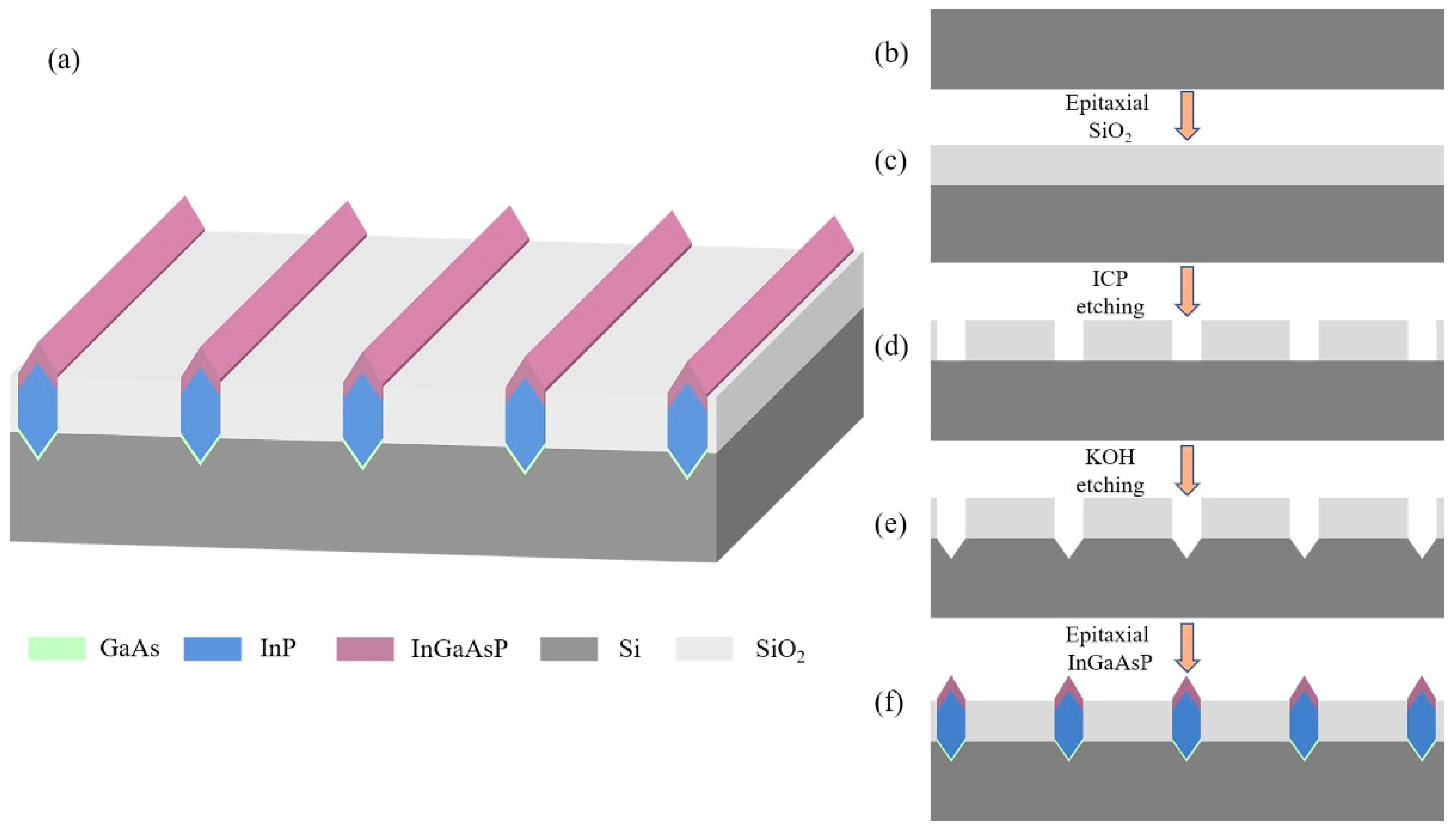
2. Materials and Methods

The materials were grown by metalorganic chemical vapor deposition (MOCVD, AIXTRON 200, Herzogenrath, Germany). Figure 1b–f charts the epitaxial process. First, silicon oxide was grown on the Si substrate (Figure 1c). The thickness of the silicon oxide was 1 μm. Photolithography was used to define the locations of trenches, and inductively coupled plasma (ICP) was used to etch trenches (Figure 1d). The trenches had a width of 500 nm, depth of 1 μm, and interval of 3.5 μm. KOH was used to etch the bottom V-shaped trench (Figure 1e). The depth of the V-shaped trench was 460 nm and the width was 500 nm. Finally, the GaAs, InP, and In1−xGaxAsyP1−y submicron wires were grown in sequence (Figure 1f). The submicron wires were 2.2 μm in height, 900 nm in width, and 1 cm in length. Triethylgallium (TEGa), trimethylgallium (TMGa), and arsine (AsH3) were used as the precursors of the GaAs buffer layer. The precursors of InP nanowires were trimethylindium (TMIn) and phosphorane (PH3). TMGa, TMIn, PH3, and AsH3 were used for the epitaxy of In1−xGaxAsyP1−y submicron wires. In1−xGaxAsyP1−y submicron wires were epitaxially grown on a Si substrate. Figure 1a shows a schematic diagram of the structure of the epitaxial In1−xGaxAsyP1−y submicron wires. In1−xGaxAsyP1−y was grown at the top of the trench. Scanning electron microscopy (SEM, NanoSEM650, FEI Company, Hillsboro, OR, USA) was used to study the morphology of In1−xGaxAsyP1−y submicron wires; we determined that the epitaxial submicron wires had a good morphology. The crystal structure and composition of the In1−xGaxAsyP1−y submicron wires were analyzed by transmission electron microscopy (TEM, JEM-F200, Akishima, Tokyo) and energy dispersive spectroscopy (EDS). The epitaxial submicron wires had a good material quality. The composition of the In1−xGaxAsyP1−y submicron wires was investigated by the composition analysis of EDS. Through high-resolution X-ray diffraction (HRXRD, Bede D1, Durham, UK) measurement, epitaxial In1−xGaxAsyP1−y was lattice-matched to epitaxial InP. Through a micro-region PL spectrum test, we found that the PL spectrum peak extended from 1260 nm to 1340 nm, thus realizing the regulation of the material energy band of the submicron wires.
Figure 2 presents a schematic diagram of the epitaxial process of the silicon-based In1−xGaxAsyP1−y submicron wires. A detailed description of In1−xGaxAsyP1−y submicron wires’ growth steps is as follows. Firstly, H2 was used as the carrier gas for thermal cleaning. The pressure of the reaction chamber was 55 mbar, and the wafer was heated to 720 °C in an H2 atmosphere to remove impurities on its surface. Secondly, the GaAs buffer layer in the V-shaped silicon trench was grown in two steps, which can improve the quality of epitaxial materials. The thickness of the LT and HT GaAs layers was 20 nm. Thirdly, a low-temperature InP nucleation layer and a high-temperature InP layer were grown [7]. The thickness of the LT and HT InP was 2 μm. Finally, after the high-temperature InP layer epitaxy was completed, the In1−xGaxAsyP1−y layer was grown at a growth temperature of 650 °C, and the thickness of the epitaxial layer was 200 nm. In this step, various epitaxy parameters were used to realize lattice-matching with the InP material and control the resulting material’s composition.

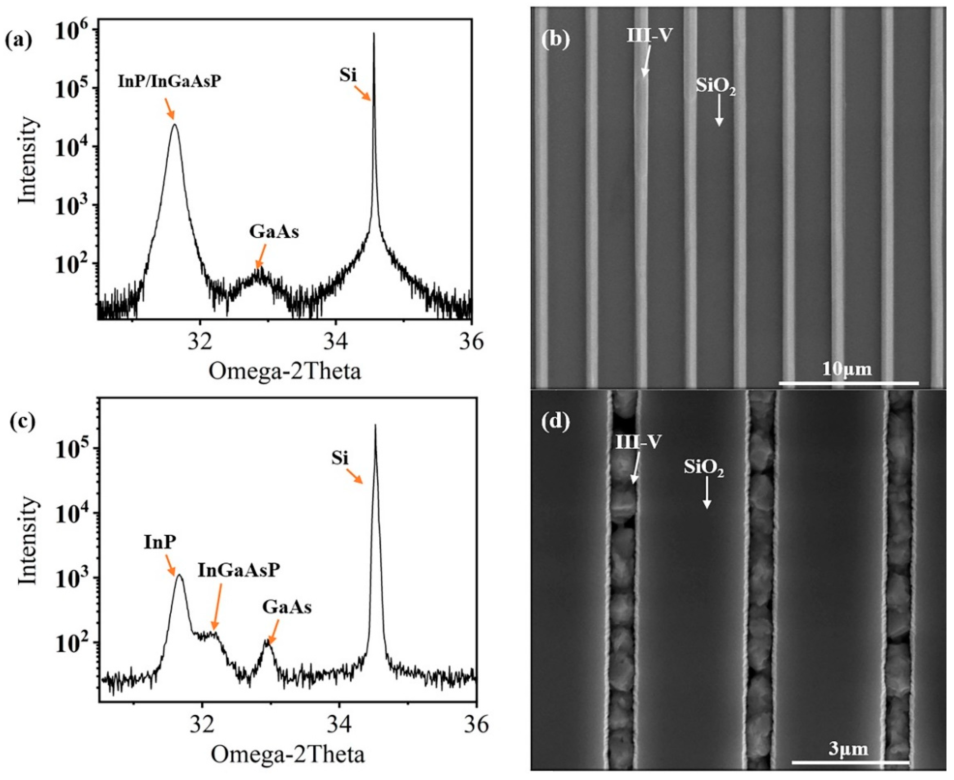
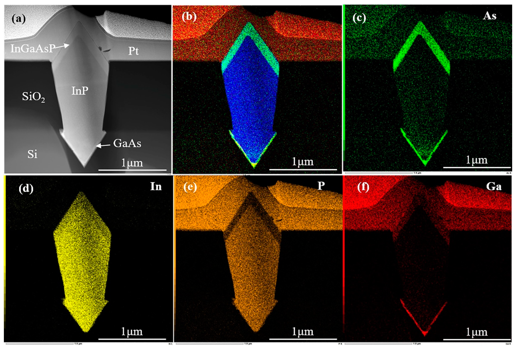
3. Results and Discussion

The HRXRD pattern was used to analyze whether the epitaxial In1−xGaxAsyP1−y matches the InP lattice. We grew In1−xGaxAsyP1−y submicron wires with various epitaxy parameters, and we used the ω-2θ scanning method to scan the diffraction peaks around the (004) Bragg reflection of the Si substrate. Figure 3a shows the HRXRD pattern of In1−xGaxAsyP1−y submicron wires when the lattice is matched. According to Figure 3a, there is only one diffraction peak at 31.7°, which is the diffraction peak of In1−xGaxAsyP1−y and InP. During the epitaxy process of In1−xGaxAsyP1−y and InP, if the crystal lattice does not match, there will be a significantly broader and two-peak overlap detected by HRXRD, and when the lattice matches, there will only be one diffraction peak. Figure 3c shows the HRXRD pattern of In1−xGaxAsyP1−y submicron wires when the lattice is not matched. According to Figure 3c, there are two diffraction peaks at 31.7° and 32.2°, which are the diffraction peaks of InP and In1−xGaxAsyP1−y. The diffraction peak at 33° is that of epitaxial GaAs, and the diffraction peak at 34.6° corresponds to the diffraction peak of the Si substrate. We changed the lattice constant of the epitaxial In1−xGaxAsyP1−y by adjusting the gas flow of the group III and V sources (different molar flows) to epitaxially modify the In1−xGaxAsyP1−y submicron wire that matches the InP lattice. Figure 3b is the SEM image of the In1−xGaxAsyP1−y submicron wire when the lattice is matched. It can be seen from the figure that the epitaxial submicron wire has a good morphology, which means that we successfully grew high-quality In1−xGaxAsyP1−y submicron wires that match the InP lattice. Figure 3d is the SEM image of the In1−xGaxAsyP1−y submicron wires when they do not match the InP lattice. It can be observed that the morphology of the submicron wires is very poor, and the strain on the material is large, similar to the formation of polycrystalline, so the material does not grow well.
TEM and EDS analyses were carried out to further understand the chemical composition and crystal defects of the In1−xGaxAsyP1−y submicron wires matched with the InP lattice. Figure 4a is a cross-sectional TEM image of the In1−xGaxAsyP1−y submicron line. The material in the In1−xGaxAsyP1−y layer is of good quality without obvious crystal defects. The Pt layer in Figure 4a is platinum deposited during TEM preparation to serve as a protective layer for the submicron wires. Figure 4b is a superimposed view of each element after EDS surface scanning. It can clearly be seen for the epitaxial GaAs, InP, and In1−xGaxAsyP1−y materials that the boundaries of each epitaxial layer are obvious. Figure 4c–f shows EDS surface scanning of the element distribution of As (green), In (yellow), P (orange), and Ga (red). The distribution of each element can be seen from the EDS energy spectrum. Different epitaxial layers can be determined by different elements. In Figure 4c,f, the GaAs buffer layer—epitaxially at the bottom of the V-shaped trench—can be seen as a very thin epitaxial buffer layer. It can be seen from Figure 4d,e that the epitaxial InP layer on the GaAs buffer layer has a good morphology. In Figure 4c–f, we can see the In1−xGaxAsyP1−y layer epitaxially on the InP layer. The interface between the In1−xGaxAsyP1−y layer and the InP layer can be seen more clearly in Figure 4c,f.
EDS line scanning was used on the epitaxial region of the In1−xGaxAsyP1−y material. Figure 5a is a TEM image of the epitaxial In1−xGaxAsyP1−y material region, and we can see an obvious interface between the In1−xGaxAsyP1−y layer and the InP layer. Figure 5b is the result of the EDS line scan. The position of the line scan is along the orange line in Figure 5a, and the scanning direction is from left to right. The scan range covered the whole of In1−xGaxAsyP1−y. The four different color lines in the scan results correspond to the four different elements, respectively: P (blue), Ga (red), As (green), and In (yellow). The horizontal axis is the distance from left to right, and the vertical axis is the relative intensity. From the results for the P and In elements, it can be seen that the distribution in the InP layer is very balanced, while the As and Ga elements are not distributed in the InP layer. In the In1−xGaxAsyP1−y layer, the In and P elements are significantly reduced while the Ga and As elements are significantly distributed. It can clearly be concluded that the In1−xGaxAsyP1−y material was successfully grown. According to their intensity in the figure, the interfaces are sharp enough to clearly distinguish between In1−xGaxAsyP1−y and the InP layers.
In this work, we adjusted the x and y values in the epitaxial In1−xGaxAsyP1−y submicron wire by changing the gas flow rates of the group III and V sources (different molar flows) during epitaxy, to adjust the material bandgap width. In1−xGaxAsyP1−y (0 ≤ x ≤ 0.47; 0 ≤ y ≤ 1) matched with the InP lattice covers the 0.91–1.67 μm band and is widely used in the production of semiconductor lasers.
The relationship between the bandgap (Eg) and composition of In1−xGaxAsyP1−y can be expressed as [22]:
E g ( x , y ) = 1.35 + 0.688 x 1.17 y + 0.758 x 2 + 0.18 y 2 0.069 x y 0.322 x 2 y + 0.03 x y 2
The relationship between x and y of In1−xGaxAsyP1−y (0 ≤ x ≤ 0.47; 0 ≤ y ≤ 1) matched with the InP lattice is:
x 0.1894 y / ( 0.4184 0.0130 y ) , ( 0 y 1 )
Taking the value of x in Formula (2) over into Formula (1), the bandgap of In1−xGaxAsyP1−y matched with the InP lattice is:
E g ( y ) = 1.35 0.775 y + 0.149 y 2
The bandgap of In1−xGaxAsyP1−y can be calculated from the PL spectrum. After that, the relevant components of the material can be calculated using Formulas (2) and (3) [21]. According to the calculation, the compositions of the material at different molar flows of the group III and V sources are obtained; the results are shown in Table 1. At the same time, we tested the room temperature PL spectrum of the epitaxial In1−xGaxAsyP1−y submicron wires under different molar flow conditions. The 532 nm laser used as the excitation source was focused by the objective lens, and the focused spot was irradiated at the sample surface. The excited PL light was collected by the same objective lens and then guided to the spectrometer, as selected with a 150-line/mm grating and an InGaAs detector cooled by liquid nitrogen. The PL spectra of the submicron wires under different molar flows differed, with the PL spectrum peaks between 1260 and 1340 nm. The lines of different colors in Figure 6 correspond to the PL spectra of submicron wires with different molar flow conditions. The compositions of the submicron wires corresponding to the four lines in Figure 6 are shown in Table 1. The PL spectrum peaks of the four submicron wires were 1340 nm, 1300 nm, 1275 nm, and 1260 nm, respectively. We found that by adjusting the molar flow of epitaxial In1−xGaxAsyP1−y, the composition of the material could be successfully changed, and the bandgap of the material was changed at the same time. With a decrease in the molar flow of the Ga source and AsH3, the In and P compositions gradually increased, and the Ga and As compositions gradually decreased, too. At the same time, the PL peak gradually decreased. We successfully realized the epitaxy of In1−xGaxAsyP1−y submicron wires with different bandgap widths; the adjustment range reached 80 nm, which can be successfully applied in our future epitaxial structural design work.

4. Conclusions

In summary, we succeeded in obtaining epitaxial In1−xGaxAsyP1−y submicron wires on Si substrates using the ART method. By changing the molar flow rates of the group III and V sources, control of the material composition of the In1−xGaxAsyP1−y submicron wire was achieved. Under optimized growth conditions, submicron wires that match the InP lattice can be epitaxially grown, and the quality of the submicron wires is very high. Through a room temperature micro-area PL spectrum test, it was found that the PL peaks of the In1−xGaxAsyP1−y submicron wires, epitaxial at different growth parameters, range from 1260 nm to 1340 nm, which demonstrates the successful control of the material bandgap width of the submicron lines. The research presented here represents a preliminary effort to prepare for future epitaxy work.

Author Contributions

Conceptualization, W.Y. and Z.Y.; methodology, M.W., H.Y. and Y.Z.; validation, W.Y., Z.Y. and W.W.; formal analysis, W.Y. and Z.Y.; investigation, W.Y. and Z.Y.; resources, X.Z. and J.P.; data curation, W.Y. and Z.Y.; writing—original draft preparation, W.Y.; writing—review and editing, W.Y., X.Z. and J.P.; visualization, W.Y.; supervision, X.Z. and J.P.; project administration, X.Z. and J.P.; funding acquisition, X.Z. and J.P. All authors have read and agreed to the published version of the manuscript.

Funding

This research was funded by the National Key Technology R&D Program (grant no. 2018YFA0209001), Frontier Science Research Project of CAS (grant no. QYZDY-SSW-JSC021), and Strategic Priority Research Program of CAS (grant no. XDB43020202).

Institutional Review Board Statement

Not applicable.

Informed Consent Statement

Not applicable.

Data Availability Statement

Not applicable.

Conflicts of Interest

The authors declare no conflict of interest.

References

  1. Hoefflinger, B. ITRS: The International Technology Roadmap for Semiconductors. In Chips 2020: A Guide to the Future of Nanoelectronics; Hoefflinger, B., Ed.; Springer: Berlin/Heidelberg, Germany, 2012; pp. 161–174. [Google Scholar]
  2. Krishnamoorthy, A.V.; Ho, R.; Zheng, X.; Schwetman, H.; Lexau, J.; Koka, P.; Li, G.L.; Shubin, I.; Cunningham, J.E. Computer Systems Based on Silicon Photonic Interconnects. Proc. IEEE 2009, 97, 1337–1361. [Google Scholar] [CrossRef]
  3. Gunn, C. CMOS Photonics for High-speed Interconnects. IEEE Micro 2006, 26, 58–66. [Google Scholar] [CrossRef]
  4. Offrein, B.J. Silicon Photonics for the Data Center. In Proceedings of the Optical Fiber Communications Conference & Exhibition, Los Angeles, CA, USA, 22–26 March 2015; p. W3A.4. [Google Scholar]
  5. Wang, X.J.; Zhaotang, S.U.; Zhou, Z.P. Recent progress of silicon photonics. Sci. Sin. Phys. Mech. Astron. 2015, 45, 014201. [Google Scholar]
  6. Duprez, H.; Descos, A.; Ferrotti, T.; Harduin, J.; Bakir, B. Heterogeneously Integrated III-V on Silicon Distributed Feedback Lasers at 1310 nm. In Proceedings of the Optical Fiber Communication Conference and Exposition (OFC 2015), Los Angeles, CA, USA, 22–26 March 2015. [Google Scholar]
  7. Liao, M.; Chen, S.; Hou, S.; Chen, S.; Wu, J.; Tang, M.; Kennedy, K.; Li, W.; Kumar, S.; Martin, M. Monolithically Integrated Electrically Pumped Continuous-Wave III-V Quantum Dot Light Sources on Silicon. IEEE J. Sel. Top. Quantum Electron. 2017, 23, 16904546. [Google Scholar] [CrossRef] [Green Version]
  8. Fiorenza, J.; Park, J.S.; Hydrick, J.; Li, J.; Li, J.; Curtin, M.; Carroll, M.; Lochtefeld, A. Aspect Ratio Trapping: A Unique Technology for Integrating Ge and III-Vs with Silicon CMOS. ECS Trans. 2010, 33, 963. [Google Scholar] [CrossRef]
  9. Li, J.; Bai, J.; Hydrick, J.M.; Fiorenza, J.G.; Major, C.; Carroll, M.; Shellenbarger, Z.; Lochtefeld, A. Thin Film InP Epitaxy on Si (001) Using Selective Aspect Ratio Trapping. ECS Trans. 2009, 18, 887–894. [Google Scholar] [CrossRef]
  10. Li, Q.; Ng, K.W.; Lau, K.M. Growing antiphase-domain-free GaAs thin films out of highly ordered planar nanowire arrays on exact (001) silicon. Appl. Phys. Lett. 2015, 106, 072105. [Google Scholar] [CrossRef] [Green Version]
  11. Wang, G.; Leys, R.R.; Loo, R.; Richard, R.; Bender, R.; Waldron, R.; Brammertz, R.; Dekoster, J.; Wang, R.; Seefeldt, R.J.A.P.L. Selective area growth of high quality InP on Si (001) substrates. Appl. Phys. Lett. 2010, 97, 121913. [Google Scholar] [CrossRef]
  12. Li, S.; Zhou, X.; Kong, X.; Li, M.; Mi, J.; Bian, J.; Wang, W.; Pan, J. Evaluation of growth mode and optimization of growth parameters for GaAs epitaxy in V-shaped trenches on Si. J. Cryst. Growth 2015, 426, 147–152. [Google Scholar] [CrossRef]
  13. Li, S.-Y.; Zhou, X.-L.; Kong, X.-T.; Li, M.-K.; Mi, J.-P.; Bian, J.; Wang, W.; Pan, J.-Q. Selective Area Growth of GaAs in V-Grooved Trenches on Si(001) Substrates by Aspect-Ratio Trapping. Chin. Phys. Lett. 2015, 32, 028101. [Google Scholar] [CrossRef]
  14. Li, S.; Zhou, X.; Kong, X.; Li, M.; Mi, J.; Pan, J. Catalyst-free growth of InP nanowires on patterned Si (001) substrate by using GaAs buffer layer. J. Cryst. Growth 2016, 440, 81–85. [Google Scholar] [CrossRef]
  15. Li, S.; Zhou, X.; Li, M.; Kong, X.; Mi, J.; Wang, M.; Wang, W.; Pan, J. Ridge InGaAs/InP multi-quantum-well selective growth in nanoscale trenches on Si (001) substrate. Appl. Phys. Lett. 2016, 108, 021902. [Google Scholar] [CrossRef]
  16. Li, Y.; Wang, M.; Zhou, X.; Wang, P.; Yang, W.; Meng, F.; Luo, G.; Yu, H.; Pan, J.; Wang, W. InGaAs/InP multi-quantum-well nanowires with a lower optical leakage loss on v-groove-patterned SOI substrates. Opt. Express 2019, 27, 494–503. [Google Scholar] [CrossRef] [PubMed]
  17. Han, Y.; Ng, W.K.; Xue, Y.; Li, Q.; Wong, K.S.; Lau, K.M. Telecom InP/InGaAs nanolaser array directly grown on (001) silicon-on-insulator. Opt. Lett. 2019, 44, 767–770. [Google Scholar] [CrossRef] [PubMed]
  18. Han, Y.; Ng, W.K.; Xue, Y.; Wong, K.S.; Lau, K.M. Room temperature III–V nanolasers with distributed Bragg reflectors epitaxially grown on (001) silicon-on-insulators. Photonics Res. 2019, 7, 1081–1086. [Google Scholar] [CrossRef] [Green Version]
  19. Shi, Y.; Wang, Z.; Van Campenhout, J.; Pantouvaki, M.; Guo, W.; Kunert, B.; Van Thourhout, D. Optical pumped InGaAs/GaAs nano-ridge laser epitaxially grown on a standard 300-mm Si wafer. Optica 2017, 4, 1468–1473. [Google Scholar] [CrossRef]
  20. Tian, B.; Wang, Z.; Pantouvaki, M.; Absil, P.; Van Campenhout, J.; Merckling, C.; Van Thourhout, D. Room Temperature O-band DFB Laser Array Directly Grown on (001) Silicon. Nano Lett. 2017, 17, 559–564. [Google Scholar] [CrossRef] [PubMed]
  21. Levinstein, M.; Rumyantsev, S.; Shur, M. Handbook Series on Semiconductor Parameters; World Scientific: Singapore, 1996. [Google Scholar]
  22. Zilko, J.L.; Davisson, P.S.; Luther, L.; Trapp, K.D.C. Improved compositional uniformity of InGaAsP grown by low pressure metalorganic vapor phase epitaxy using tertiary butyl phosphine as the phosphorus source. J. Cryst. Growth 1992, 124, 112–117. [Google Scholar] [CrossRef]
Figure 1. (a) Schematic diagram of the In1−xGaxAsyP1−y submicron wire structure; (bf) Flow diagram of the epitaxial process of the epitaxial submicron wires.
Crystals 12 00476 g001
Figure 2. Schematic diagram of the epitaxy process of silicon-based In1−xGaxAsyP1−y submicron wires.
Crystals 12 00476 g002
Figure 3. (a) HRXRD pattern of In1−xGaxAsyP1−y submicron wire when the lattice is matched; (b) SEM image of In1−xGaxAsyP1−y submicron wire when the lattice is matched; (c) HRXRD pattern of In1−xGaxAsyP1−y submicron wire when the lattice is not matched; (d) SEM image of In1−xGaxAsyP1−y submicron wire when the lattice is not matched.
Crystals 12 00476 g003
Figure 4. (a) In1−xGaxAsyP1−y submicron wire cross-section TEM image from an EDS surface scan; (b) Superimposed view of all elements, and single views of (c) As, (d) In, (e) P, and (f) Ga.
Crystals 12 00476 g004
Figure 5. (a) TEM image and (b) EDS line scan result of the epitaxial region of the In1−xGaxAsyP1−y material.
Crystals 12 00476 g005
Figure 6. PL spectra of epitaxial In1−xGaxAsyP1−y materials under different molar flows.
Crystals 12 00476 g006
Table 1. In1−xGaxAsyP1−y submicron wires with different molar flows.
In1−xGaxAsyP1−yGaInAsP
Gas Molar Flow(mol/min)
1nTMGa = 3.9 × 10⁻⁶ nTMIn = 9.4 × 10⁻⁶
nAH3 = 3.1 × 10⁻⁴ nPH3 = 4.5 × 10⁻³
0.2870.7130.6220.378
2nTMGa = 2.8 × 10⁻⁶ nTMIn = 9.4 × 10⁻⁶
nAH3 = 2.2 × 10⁻⁴ nPH3 = 4.5 × 10⁻³
0.2650.7350.5750.425
3nTMGa = 2.2 × 10⁻⁶ nTMIn = 9.4 × 10⁻⁶
nAH3 = 1.8 × 10⁻⁴ nPH3 = 4.5 × 10⁻³
0.2480.7520.5380.462
4nTMGa = 1.1 × 10⁻⁶ nTMIn = 9.4 × 10⁻⁶
nAH3 = 8.9 × 10⁻⁵ nPH3 = 4.5 × 10⁻³
0.2420.7580.5250.475
Publisher’s Note: MDPI stays neutral with regard to jurisdictional claims in published maps and institutional affiliations.

