Article

Role of Oxygen and Fluorine in Passivation of the GaSb(111) Surface Depending on Its Termination

by
Alexander V. Bakulin
1,*,
Lora S. Chumakova
1,
Aleksandr V. Korchuganov
1 and
Svetlana E. Kulkova
1,2
1
Institute of Strength Physics and Materials Science, Siberian Branch of Russian Academy of Sciences, pr. Akademichesky 2/4, 634055 Tomsk, Russia
2
Physics Department, National Research Tomsk State University, pr. Lenina 36, 634050 Tomsk, Russia
*
Author to whom correspondence should be addressed.
Crystals 2022, 12(4), 477; https://doi.org/10.3390/cryst12040477
Submission received: 28 February 2022 / Revised: 29 March 2022 / Accepted: 29 March 2022 / Published: 30 March 2022

Abstract

:
The mechanism of the chemical bonding of oxygen and fluorine on the GaSb(111) surface depending on its termination is studied by the projector augmented-waves method within density functional theory. It is shown that on an unreconstructed (111) surface with a cation termination, the adsorption of fluorine leads to the removal of surface states from the band gap. The binding energy of fluorine on the cation-terminated surface in the most preferable Ga-T position is lower by ~0.4 eV than that of oxygen, but it is significantly lower (by ~0.8 eV) on the anion-terminated surface. We demonstrate that the mechanism of chemical bonding of electronegative adsorbates with the surface has an ionic–covalent character. The covalence of the O–Sb bond is higher than the F–Sb one, and it is higher than both O–Ga and F–Ga bonds. Trends in the change in the electronic structure of the GaSb(111) surface upon adsorption of fluorine and oxygen are discussed. It is found that an increase in the oxygen concentration on the Sb-terminated GaSb(111) surface promotes a decrease in the density of surface states in the band gap.

1. Introduction

The study of the atomic and electronic structure of the surfaces of AIIIBV semiconductors is fundamentally important for technological applications in microelectronics and the improvement in modern nanotechnologies, as well as for the development of novel semiconductor materials based on them [1,2,3,4]. It is known that metal–insulator–semiconductor (MIS) heterostructures are used in the production of devices in microelectronics. The key problem for such MIS structures is the formation of the insulator–semiconductor interface with a low density of interface states [5].
There are various ways of modifying semiconductor surfaces, which can lower the density of surface states (DSS) [5,6], one of which is associated with a change in the chemical composition of the oxidizing medium. In a number of works [7,8] and references therein, it was shown that the fluorination of GaAs, InAs, and other AIIIBV semiconductor surfaces leads to a significant decrease in the DSS. It was found in [9,10,11,12,13,14] that an intermediate fluorine-containing anodic oxide layer is formed at the oxide–semiconductor interface, which contributes to a decrease in the density of surface states. Moreover, it was shown that the formed oxide layers on the semiconductor surface contain Group III element fluorides and Group V element oxyfluorides. Since it is rather difficult to establish the nature of the states in the forbidden gap by experimental methods, the use of theoretical methods is required. It is obvious that the complex composition of the transition region between the native oxide and the semiconductor makes it difficult to carry out the corresponding theoretical calculations. At the same time, it is possible in a theoretical approach to establish the effect of electronegative adsorbates (F and O) on surface states.
It should also be noted that the properties of the surfaces of AIIIBV binary semiconductor compounds significantly depend on their orientation, termination, and reconstruction, as well as existing defects [15]. Although the properties of ideal and reconstructed surfaces of AIIIBV semiconductors have been intensively studied by methods within the density functional theory, there are currently not enough works in which the adsorption of oxygen or fluorine has been studied [16,17,18,19,20,21,22,23,24,25,26]. In our early works [20,21,22,23,24,25,26,27], we studied the interaction of halogens (F, Cl, Br, I) with the AIIIBV(001) and (111) surfaces. It was found that, irrespective of the reconstruction of the AIIIBV surface, halogens prefer to form bonds with cations. The adsorption of oxygen and the co-adsorption of fluorine on the cation-terminated surface were studied in [21,25,26,27]. In particular, in [21], the oxygen binding energy on the unreconstructed InAs(111) − (1 × 1)and reconstructed (2 × 2) surfaces was studied. It was shown that the adsorption of atomic oxygen in all considered positions leads to the appearance of surface states in the band gap, in contrast to the results obtained on the GaAs(001) surface [16,17,18]. However, with an increase in the oxygen concentration, defect states on the reconstructed In-terminated InAs(111) surface [21] are localized only at the Brillouin zone boundary and shift to the bottom of the conduction band (CB) or to the top of the valence band (VB).
When fluorine is adsorbed on both unreconstructed and reconstructed In-terminated InAs(111) surfaces, the surface states induced by oxygen adsorption are completely or partially removed from the band gap if fluorine forms bond with surface indium atoms. A similar situation was observed on the Ga-terminated GaAs(111) surface [25]. It is interesting to note that the sequence of adsorption of fluorine and oxygen insignificantly affects the surface states in the band gap [26]. In [27], the effect of the anion on the revealed peculiarities upon fluorine and oxygen co-adsorption and on the electronic energy spectrum of the cation-terminated InSb(111) surface was studied. It was also established that oxygen-induced surface states are completely or partially removed from the band gap during O and F co-adsorption depending on the fluorine concentration. On the whole, observed significant structural changes in the near-surface layers of the semiconductor are due to the penetration of adsorbates in the substrate that leads to the breaking of the In–Sb bonds and the formation of new F–Sb and O–Sb bonds. The latter can be considered as the initial stage of the formation of a fluorine-containing anodic oxide layer. At the same time, adsorption of oxygen alone leads to opposite effects depending on the termination of the InSb(111) surface; additional states appear in the band gap in the case of the In-termination, whereas the density of surface states decreases on the Sb-termination of the surface [27].
At present, it remains unclear whether the replacement of the cation will lead to a change in the features of the effect of oxygen on the electronic structure of the anion-terminated AIIIBV(111) surface. In this regard, the aim of present work is to study the electronic properties of the GaSb(111) surface upon the adsorption of oxygen and fluorine in order to reveal the effect of the cation on the mechanisms of surface passivation depending on its termination.

2. Computational Details

Calculations of the atomic and electronic structure of the GaSb(111) surface, as well as the bulk semiconductor, were carried out by the projector augmented-wave (PAW) method in a plane-wave basis [28,29] implemented by VASP code [30]. A generalized gradient approximation for the exchange-correlation (XC) function in the form of GGA–PBE [31] was applied. It is known that GaSb has a zincblende structure (B3, space group 216– F 4 ¯ 3 m ), with gallium atoms occupying 4a Wyckoff positions, and antimony atoms–4c (Figure 1a). The theoretical lattice parameter of GaSb, equal to 6.236 Å, is in agreement with the experimental value of 6.096 Å [32]. For visualization of the atomic structure and electron density distribution, the VESTA program was used [33].
In the <111> direction, the atomic structure of the semiconductor is an alternation of atomic layers of Ga and Sb, and the [111] and [ 1 ¯ 1 ¯ 1 ¯ ] directions are nonequivalent (Figure 1b,c). In accordance with commonly used notation of the AIIIBV surface with {111} orientation (e.g., [34]), the Ga-terminated (111) surface is called GaSb(111)A, and the Sb-terminated ( 1 ¯ 1 ¯ 1 ¯ ) one – GaSb(111)B. In the present calculation, the GaSb(111) – (1 × 1) surface was simulated by eight-layer films. The distance between the films in two adjacent cells along the z axis was no less than 10 Å, which allowed us to exclude the interaction between them. The dangling bonds of Sb (Ga) atom on one side of the film were saturated with pseudo-hydrogen atoms (one H* atom for each Sb (Ga) atom) with a fractional charge of 0.75e (1.25e) [35]; therefore, this side of the film was bulk-like. The equilibrium Sb–H* (Ga–H*) bond length was 1.761 Å (1.604 Å). The positions of the pseudo-hydrogen atoms, as well as the atoms of the two nearest atomic layers, Ga and Sb, were fixed, while the positions of the atoms of other layers were optimized until the forces at the atoms were less than 0.01 eV/Å. The maximum energy of plane waves from the basis set was 500 eV. Integration over the Brillouin zone was carried out using a 7 × 7 × 1 k-point grid generated by the Monkhorst–Pack scheme [36].
The binding energy of oxygen/fluorine atoms with the substrate was calculated using the following formula:
E b = E O / F + E GaSb E ( O / F ) / GaSb
where E((O/F)/GaSb) is the total energy of the system with the adsorbed oxygen or fluorine atom, E(GaSb) is the total energy of the surface without the adsorbate, and E(O/F) is the energy of the oxygen/fluorine atoms.
Note that the DFT–1/2 method was also used to calculate the electronic spectrum of a bulk semiconductor and its surface, which assumes the use of the standard Kohn–Sham potential with eigenvalues obtained for the potential of a partially ionized anion. In our case, the occupancy of the 5p shell of antimony was 2.5 electrons instead of 3. Details of the DFT–1/2 method can be found in [37,38,39,40]. Here, we note that the Coulomb potential of such an anion is replaced by some short-range potential by multiplying the former by a function of the form [1 − (r/rcut)n]3, where rcut is the cutoff radius (for r = rcut, the Coulomb potential tends to zero), and n is a parameter that controls the damping rate.
The value of the cutoff radius rcut is chosen so that it corresponds to the maximum value of the band gap (Eg) of the semiconductor, and the value of n should be as large as possible. In calculations, as a rule, n = 8 is chosen, but for compounds with covalent or weakly ionic bonds, the value of n should be increased if there are no problems with convergence [40]. The obtained values of the band gap width in the case of a bulk GaSb compound for n = 8, 25, and 50, depending on rcut, are shown in Figure 2a. It is seen that even in the case n = 50, the band gap was ~19% less than the experimental value of 0.812 eV [32]. In this case, the degeneracy of states at the Γ point near the Fermi level (EF) was removed in the electronic energy spectrum of semiconductor (Figure 2c). Note that the HSE06 hybrid functionals [41] and metaGGA (mBJ) [42] also partially solved the problem of the band gap width (Figure 2b,d), but the former significantly increased the computation time, and the latter had problems with convergence in the case of low-dimensional systems with vacuum. In this work, we used the values rcut = 1.9 Å and n = 50.

3. Results and Discussion

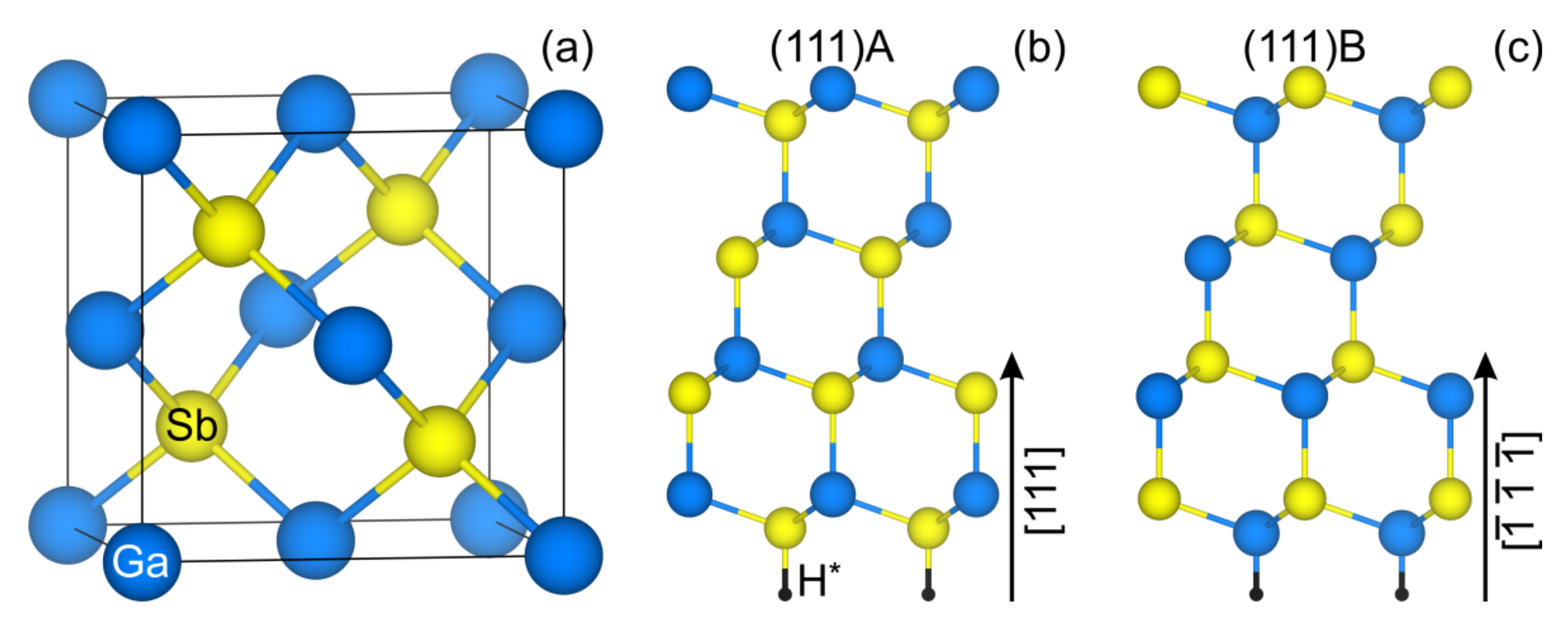
3.1. Atomic and Electronic Structure of Clean GaSb(111) Surface

The relaxation of the interlayer distances in the case of a clean GaSb(111) surface was calculated using the following formula:
Δ i j = d i j d / d
where d is the distance between the atomic planes in the bulk, and dij is the distance between the atomic layers i and j. The results are presented in Table 1 in comparison with the corresponding data for other AIIIBV semiconductors. It is seen that regardless of the GaSb(111) surface termination, the relaxation had an alternating character and decayed deep into the film. The first interlayer distance was compressed in the case of the GaSb(111)A surface. A similar behavior was observed in the case of the cation-terminated InAs(111), GaAs(111), and InSb(111) surfaces [25,27]. One can see from Table 1 that the compression of d12 correlated with the ionicity of the anion–cation chemical bond (with the difference in the electronegativity of the anion and cation, Δχ). An increase in the ionicity of a bond led to an increase in its “rigidity”, which contributed to a decrease (in modulus) of Δ12. At the same time, in the case of the GaSb(111)B surface, the relaxation had the opposite sign in comparison with GaSb(111)A.
It is seen in Figure 3a that in the case of the GaSb(111)A surface, there was one partially filled band (curve 1), which was responsible for pinning of the Fermi level. It was located near the bulk conduction band minimum and spread over almost the whole two-dimensional Brillouin zone (2D BZ). Note that hereinafter, the projection of the bulk states is shown by gray filling, and the surface states of the Ga and Sb atoms are given by blue and yellow balls, respectively. The size of these balls was proportional to the degree of localization of the electronic states on the corresponding atoms. The spectrum of the surface and the bulk state projection was adjusted by the low-lying Sb s-states. It is seen in Figure 3b that the states of gallium atoms of the surface layer (Ga1) and antimony atoms of the subsurface layer (Sb2) contributed to the sharp peak of the density of surface states at the Fermi level. This conclusion was confirmed also by the calculations of surface state localization at atoms (insert in Figure 3b), which illustrates that the Ga1 pz-states (dangling bonds) and Sb2 px- and py-states (hybridized with Ga1-states) contributed to this band. A similar trend was observed in the spectrum of the cation-terminated (111) surface in the case of other AIIIBV semiconductors [25,27]. On the GaSb(111)B surface, one could see only one surface band near the Fermi level as well. It was located near the bulk valence band maximum and spread over almost the whole 2D BZ (Figure 3c). As a result, a peak in the density of surface states connected with this band can be seen in Figure 3d. This peak was mainly conditioned by Sb1 pz-states and an insignificant contribution of Ga2 px- and py-states. It should be noted that the electronic structures of both GaSb(111)A and GaSb(111)B surfaces were very similar up to the replacement of a cation by an anion and vice versa, and the only difference was in the position of the band which pinned the Fermi level.

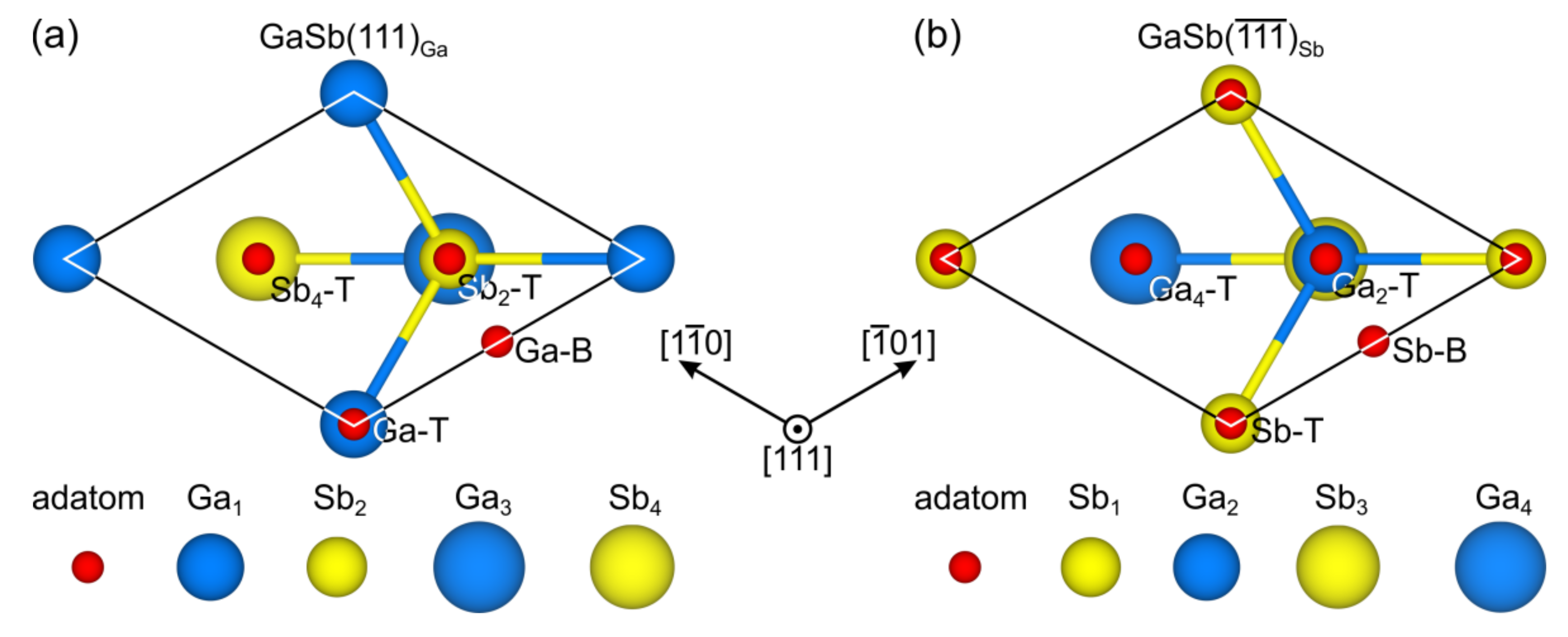
3.2. Oxygen and Fluorine Adsorption on the GaSb(111)A Surface
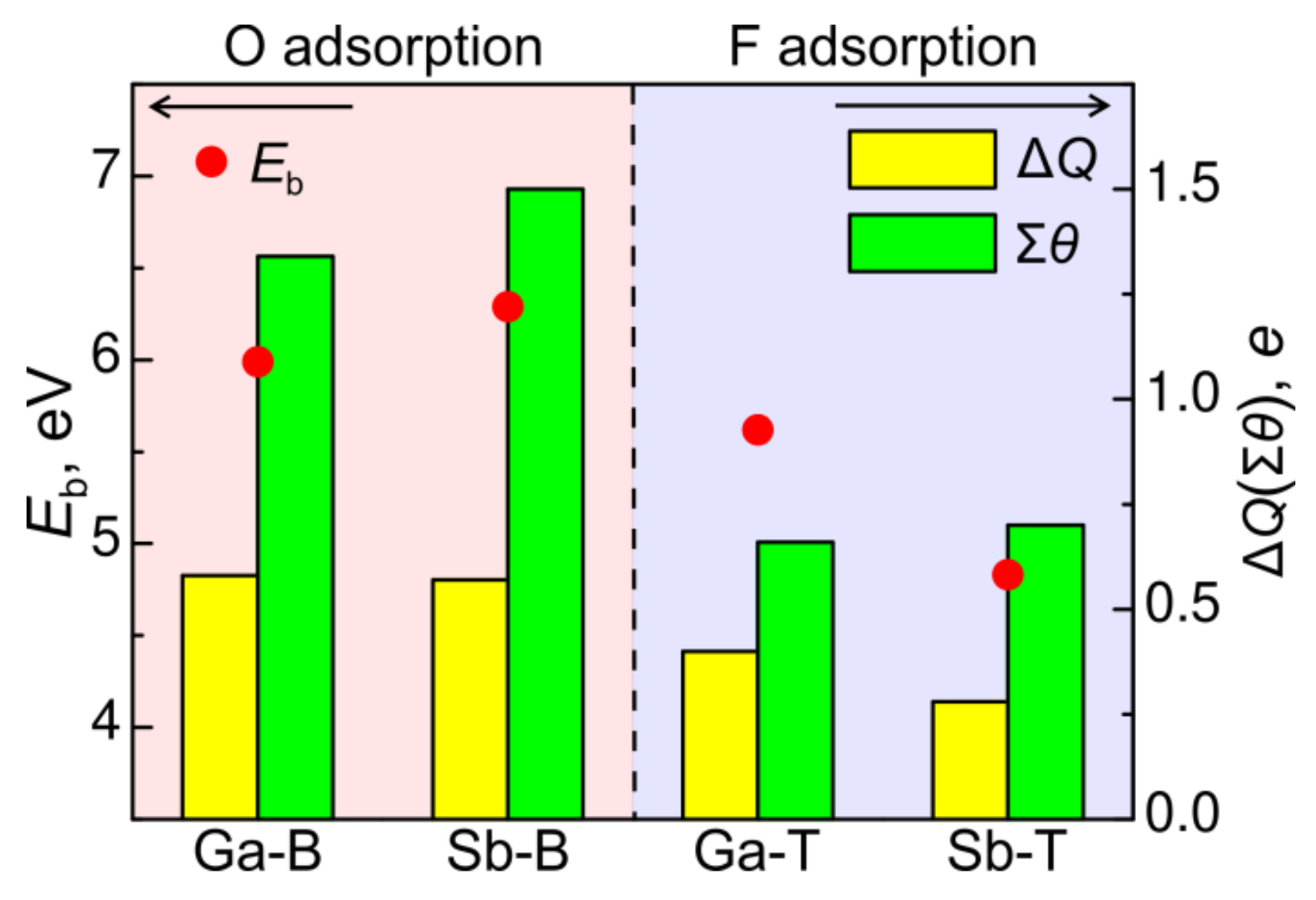
3.2.1. Oxygen

The atomic structure of the GaSb(111) surface with two possible terminations (top view) is shown in Figure 4. The considered positions of oxygen and fluorine atoms on both surfaces are also given here. On the Ga-terminated surface, the following positions were considered: the bridge position (Ga-B) between the surface gallium atoms, the top position above the surface gallium atom (Ga-T), as well as the positions above the antimony atoms of the second and fourth layers from the surface (Sb2-T and Sb4-T).
The values of oxygen binding energy for different adsorption sites on the Ga-terminated GaSb(111) surface are presented in Table 2. It is seen that oxygen had the highest binding energy in the Ga-B position. Almost the same value (5.93 eV [27]) was obtained in the case of oxygen adsorption on the InSb(111)A surface. The preference of this position for adsorption is connected with the fact that oxygen binds to two Ga1 atoms (the bond length is 2.22 Å) and an Sb2 atom (the bond length is 2.05 Å) to which it shifts during the relaxation process. It is seen from Figure 5a that the probability for oxygen to be adsorbed in the Ga-B position was substantially higher than in the other positions. It is known that the probability Ps of adsorption in position s is proportional to the binding energy in this position Eb(s). Thus, it can be estimated as the weighted arithmetic mean:
P s = n s exp E b ( s ) / k B T i n i exp E b ( i ) / k B T ,
where ni is the multiplicity of position i, kB is the Boltzmann constant, and T is temperature; the summation is carried out over all positions of adsorption.
For the other three adsorption sites on the surface, the difference in the oxygen binding energies did not exceed 0.13 eV. It should be noted that in the case of adsorption in the Sb2-T position, the oxygen atom formed a bond with the subsurface Sb2 atom (the bond length is 1.98 Å) and located by 0.2 Å below the surface layer, while in the Sb4-T position, oxygen was substantially incorporated into the substrate and was located at 1.0 Å below the surface. A slightly smaller value of 0.88 Å [27] was obtained in the case of oxygen adsorption on the InSb(111)A surface. However, oxygen located by 0.24 and 0.34 Å [25] above the surface in the case of InAs and GaAs, respectively. The reason for the oxygen penetration into the substrate is connected with larger values of the lattice parameter for semiconductors with antimony. Table 2 also lists the values of the charge transfer to oxygen atom from the substrate, the distance between the adatom and near-surface atoms, and the overlap populations of bonds (the adatom–substrate atoms). Note that both DDEC6 (Density Derived Electrostatic and Chemical) [43,44] and Bader [45] methods were used to estimate the charge transfer. The former method allows one to calculate the overlap population, but the latter was used for such estimates in our earlier works [25,27]. It is seen from Table 2 that within both approaches, similar tendencies in charge transfer were observed, although the values obtained by the Bader method were higher. The charge transfer to the adatom can serve as an indicator of the ionicity of the chemical bond, while the overlap population reflects the degree of bond covalence. The smallest charge transfer to oxygen was obtained in the Ga-T position; in this case, both Ga1 and Sb2 atoms lost their charge (~0.40e and 0.16e, respectively). At the same time, the charge states of atoms in deeper layers practically do not change. Hereinafter, the values obtained by the Bader method are discussed. Note that a direct comparison of charge transfer with the preference of positions for oxygen is difficult, since its coordination differs for different adsorption positions. In particular, in the Sb2-T and Sb4-T positions, the adatom interacts with a larger number of substrate atoms. In the most preferred Ga-B position, the contribution to charge transfer from the antimony atom is higher than that from gallium atom (0.62e and 0.21e). Overlap population analysis demonstrates that the O–Sb bond is stronger than the O–Ga bond. In general, a large charge transfer and a high overlap population indicate the ionic–covalent character of the oxygen bonding with the semiconductor substrate. In addition, the mechanical (MC) and chemical (CC) contributions to the chemical bonding of the adatom with the surface were calculated according to the model proposed by Lozovoi with co-workers [46]. It can be seen from Table 2 that, in all cases, the chemical contribution was dominant, and the greatest deformation of the substrate occurred in the case of oxygen adsorption in the Sb2-T position.

3.2.2. Fluorine

The fluorine atom needs only one electron to fill completely its p-band. As seen from Table 2, its highest binding energy with GaSb(111)A surface corresponded to the Ga-T position. We recall that the state at the Fermi level (Figure 3a) was a partially filled Ga1 pz-orbital. Since the Ga states were empty, the charge for chemical bonding with fluorine was transferred from the Sb atom of the subsurface layer due to strong hybridization of Ga1 and Sb2 states, which can be seen from Figure 3a,b. The fluorine binding energies in the other three positions were lower by 1.2–1.4 eV than in Ga-T. A similar trend takes place for other AIIIBV semiconductors also [21,25,27]. Although fluorine has a smaller atomic radius than oxygen, it did not incorporate into the substrate but located at some distance from the surface. As was shown in our earlier work [47], there are regions above the surface with a charge due to the tails of the electron wave functions. Therefore, the charge above the Sb2 and Sb4 atoms was estimated. Indeed, integrating the charge inside the sphere centered at the point corresponding to the fluorine atom in the Sb2-T or Sb4-T positions gave the values of 0.71e and 1.08e, respectively. Since the charge depends strongly on the radius of sphere, we used the ionic radius of fluorine (1.33 Å). In the case of Sb4-T position, the charge was somewhat higher, since fluorine was closer to the surface. Taking this charge, fluorine lost its reactivity.

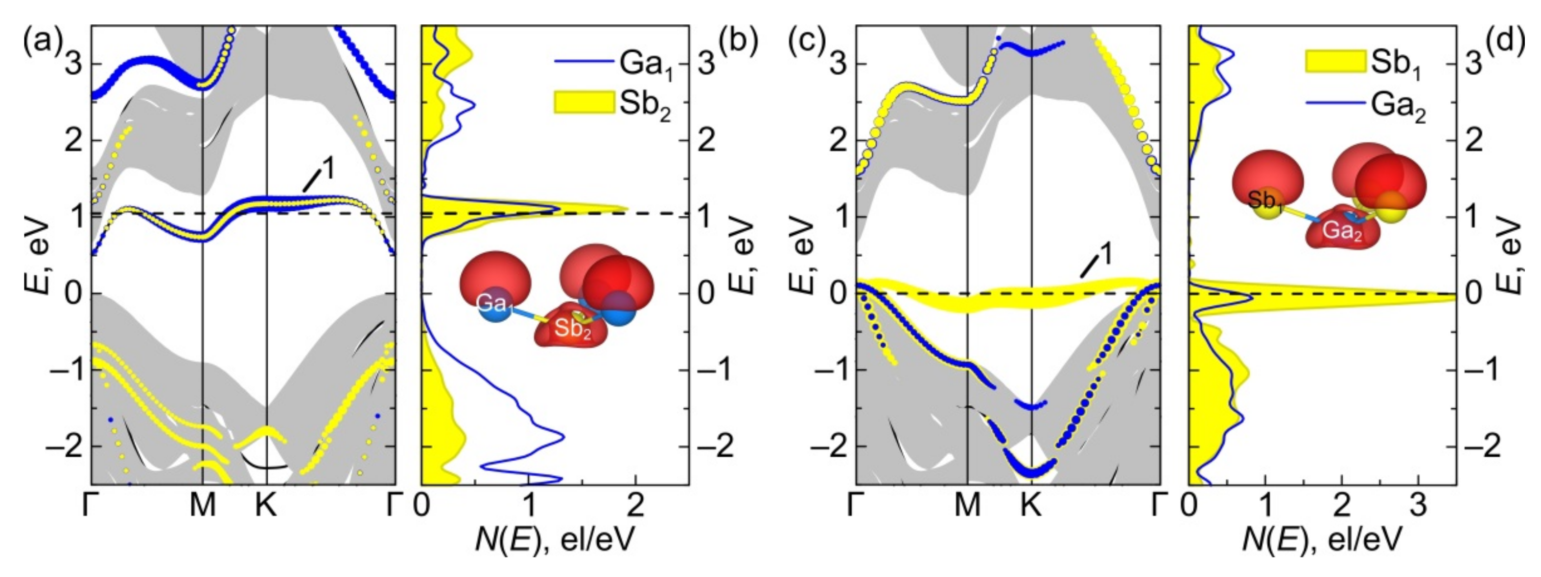
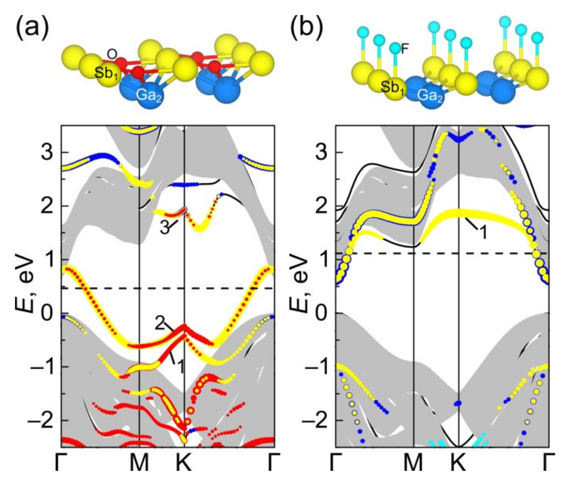
3.2.3. Electronic Energy Spectra

Figure 5 shows that oxygen and fluorine had the highest probability to be adsorbed in the Ga-B and Ga-T positions, respectively. In this section, we will discuss the features of the electronic energy spectra for these positions only. Oxygen adsorption on the GaSb(111)A surface led to the appearance of additional surface states in the band gap (Figure 6a). As was shown in [21,25,27], the structure of surface states strongly depends on the position of the adsorbate on the surface. These surface states are due to the hybridization of the O s,p-states with Ga and Sb s,p-states. It is seen in Figure 6a that the surface states localized near the Fermi level at the Γ point were predominantly due to the antimony atoms of the subsurface layer, whereas the surface states at energies of −0.8 eV and −1.0 eV (at the K point) were mixed states of oxygen and antimony atoms. Note that in the other positions, the band, which determines the pinning of the Fermi level on a clean surface (Figure 3a), was shifted towards CB, while the low lying states were shifted to the band gap. Since the structure of the energy spectra of the surface with oxygen in the Ga-T, Sb2-T, and Sb4-T positions differs only slightly from those obtained earlier for the InSb(111)A surface [27], therefore they are not presented in this work.
The electronic energy spectra of the InSb(111)A surface with fluorine atoms in several adsorption positions [27] demonstrated a lower density of surface states in the band gap, although the structure of these states strongly depends on the fluorine position. Almost the same trend was observed on the GaSb(111)A surface. Figure 6b shows that the adsorption of fluorine in the most preferred Ga-T position led to a complete depletion of the band responsible for pinning of the Fermi level on a clean surface and to an insignificant depletion of states near the VB top at the Γ point. The fluorine states were located at approximately −1.0 eV (K point) and below, whereas they were at energies of approximately −2.5 eV on the InSb(111) surface [27]. A similar effect of fluorine on the surface states was observed in the case of the semiconductors InAs and GaAs [21,25]. Note that in the latter case, the surface states of arsenic were located below the VB top at the Γ point. Moreover, in the case of the GaAs(111)A surface, the fluorine states were also located closer to the VB top at the K point, as in the present case.
We did not consider in this work the co-adsorption of fluorine and oxygen, since the obtained trends were in good agreement with the results presented earlier [21,25,27]. As in the case of the other AIIIBV semiconductors, the adsorption of fluorine on the (111)A surface completely or partially removed the surface states induced by oxygen. In general, a universal character of changes in the electron energy spectra was observed during the interaction of electronegative adsorbates with the AIIIBV(111)A surface.

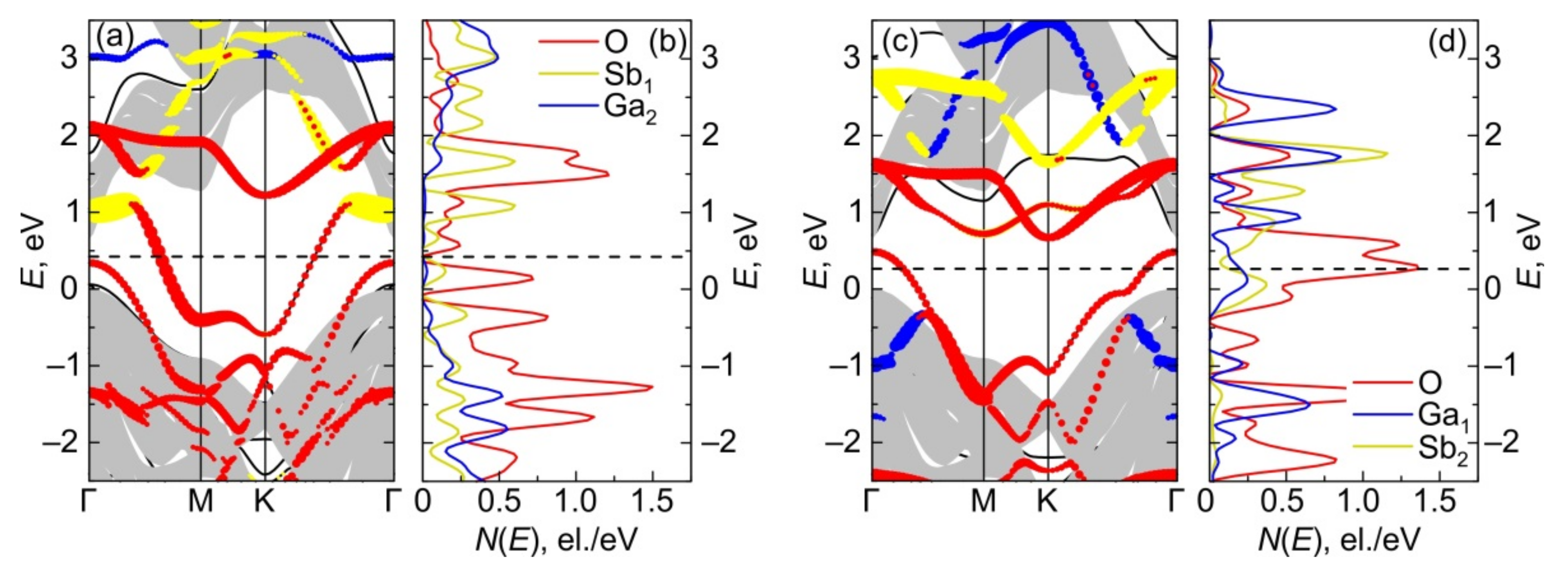
3.3. Adsorption on the GaSb(111)B Surface

In the case of the GaSb(111)B surface, the adsorption positions were the same as on the GaSb(111)A surface with the replacement of cations by anions and vice versa, i.e., Sb-B, Sb-T, Ga2-T, and Ga4-T (Figure 4b). It is seen from Table 3 that oxygen preferred to be adsorbed in the Sb-B position. The corresponding binding energy was by 0.8–1.3 eV higher than those in other positions. The binding energy of an oxygen atom above Ga2 and Ga4 atoms differed insignificantly. Thus, Figure 7a shows that the probability of oxygen adsorption in the Sb-B position was substantially higher than in other positions. The oxygen binding energy in this position on the GaSb(111)B surface was by 0.3 eV higher than the corresponding value on the GaSb(111)A one. In contrast to the cation-terminated surface, the oxygen atom incorporated into the substrate only in the case of the Ga4-T position. Fluorine on the GaSb(111)B surface preferred to be adsorbed in the Sb-T position (Figure 7b), as on the GaSb(111)A one. The binding energy was ~1.5 eV less than that of oxygen on the same surface.
It is seen from Table 3 that CC was the dominant contribution to the mechanism of the chemical bonding of both adsorbates with substrate. It is interesting that oxygen adsorption resulted in a larger deformation of the GaSb(111)A surface than that of GaSb(111)B, while in the case of fluorine, the opposite trend took place (MC in Table 2 and Table 3). The overlap population demonstrated that θ for O–Sbi bonds was higher than for O–Gai ones (i = 1, 2), irrespective of surface termination. It is seen from Figure 8 that in the case of O adsorption in the Ga(Sb)-B position, the dominant factor was hybridization of states, since a change of Eb correlated with a change of overlap population of bonds between O and surface atoms. At the same time, in the case of F adsorption in the Ga(Sb)-T position, the ionicity of chemical bonds had an important role.
The adsorption of oxygen on the GaSb(111)B surface also led to significant changes in the surface electronic structure (Figure 9a). It can be seen that there were surface states (curves 1 and 2) near the VB top, which were predominantly oxygen states at the Brillouin zone boundary in the vicinity of the K point, while the unoccupied states of curve 2 localized on the antimony atoms were concentrated at the Brillouin zone center around the Γ point. In addition, there were surface states (curve 3) near the CB bottom, which were also a consequence of the interaction of oxygen with surface antimony atoms. In this case, the states of antimony were mainly localized at the Brillouin zone boundary as well. In general, as in the case of the GaSb(111)A surface, oxygen adsorption led to depletion of the band pinning the Fermi level on the clean surface and its shift to the conduction band, while the low lying states shifted to the band gap, which resulted in re-pinning of the Fermi level.
A similar trend was observed in the case of fluorine adsorption on the surface. The antimony bands (curve 1 in Figure 9b) compared to the clean surface was strongly displaced into the conduction band. However, exactly this band pinned the Fermi level near the Γ point. Surface states of fluorine were observed mainly at the K point. It should be noted that a lower charge (0.77e) was transferred to fluorine than to oxygen (1.15e) at the same adsorption position. Thus, in contrast to the GaSb(111)A surface, on the Sb termination, the fluorine adsorption did not lead to de-pinning of the Fermi level.

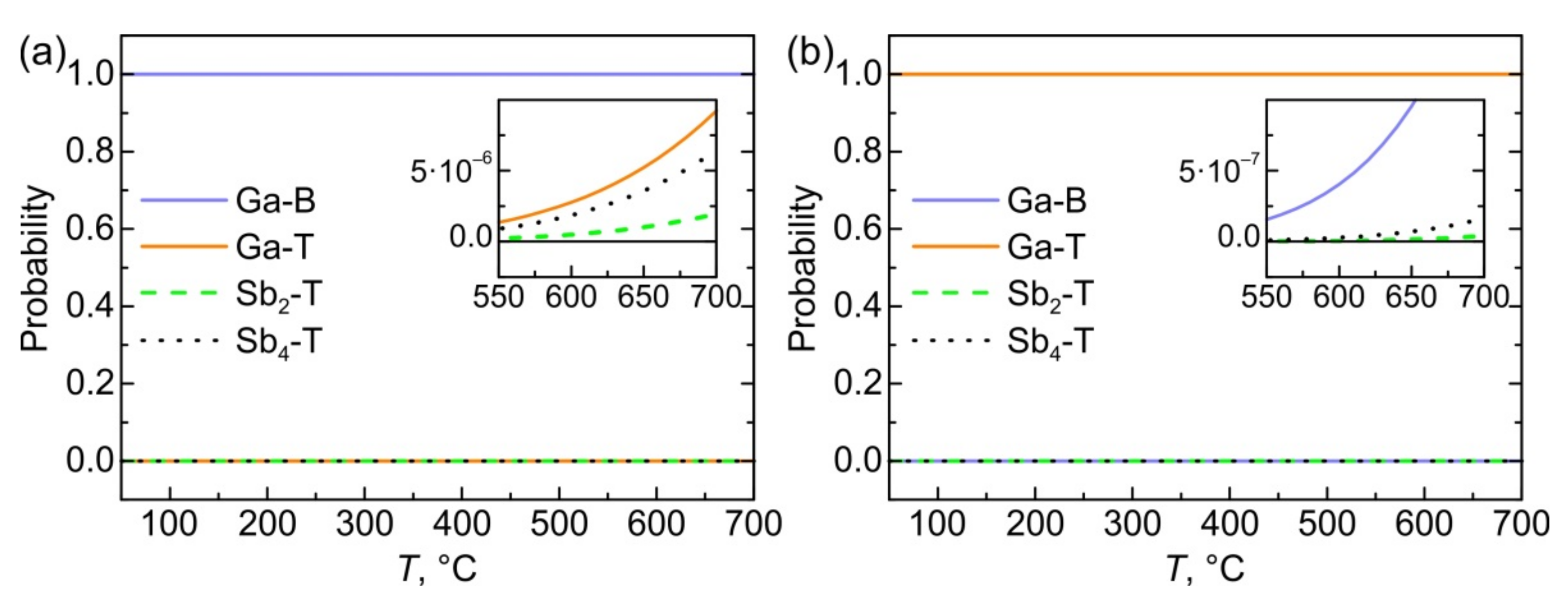
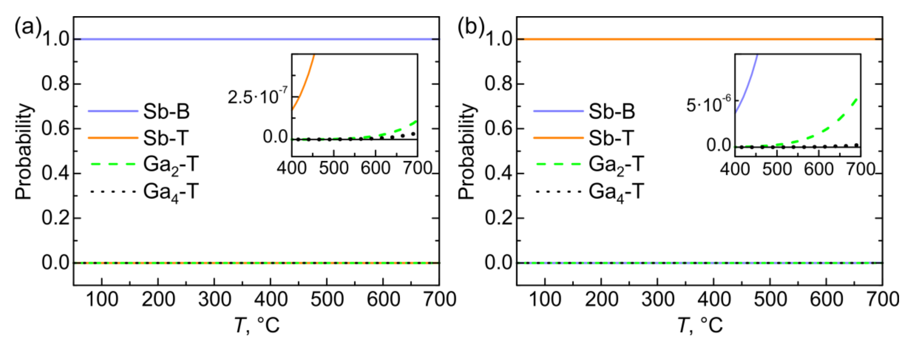
3.4. Oxygen Concentration

Finally, let us consider the effect of the oxygen concentration on the surface states in the band gap. Figure 10a shows the electron energy spectrum for the GaSb(111)B surface with three adsorbed oxygen atoms. Two additional oxygen atoms were located initially also in the most preferred Sb-B positions on the surface. It was seen that the states, which were responsible for the pinning of the Fermi level in the case of three oxygen atoms, differed insignificantly from the case of adsorption of one oxygen atom (Figure 9a). However, above the Fermi level of 1–2 eV energy, additional states localized on oxygen atoms occurred. They were shifted to the CB bottom. It should be noted that in this case, all three oxygen atoms penetrated into the substrate and located 0.78 Å below the surface. Despite the oxygen states being observed at the Fermi level, they had very low density (Figure 10b).
For comparison, Figure 10c shows an electron energy spectrum of the Ga-terminated surface with three oxygen atoms. It is seen that the electron energy spectrum had a very similar structure as in the previous case. However, in the present case, there were significantly more surface states at the Fermi level. Basically, these surface states were localized on oxygen atoms, and only states at the edge of the 2D BZ were localized on subsurface antimony atoms. The degree of their localization on Sb2 atoms was too weak, and the corresponding circles are not shown in Figure 10c. Although the structure of unoccupied surface states was similar for both surface terminations, their number in the case of the Ga-terminated surface was greater (Figure 10d). Thus, the obtained results allow us to conclude that the native oxidation of the GaSb(111)B surface leads to a decrease in the density of surface states at the Fermi level in comparison with the ideal surface. This is in agreement with earlier theoretical results obtained for InSb and with experiment [48].

4. Conclusions

The interaction of electronegative adsorbates (O and F) with the GaSb(111) surface, depending on its termination, was studied using the projector augmented-wave method. The atomic and electronic structures of the ideal surface and with adsorbates were calculated. It was shown that regardless of the surface termination, the most preferred position for oxygen adsorption is the bridge Ga(Sb)-B position between the surface gallium (antimony) atoms, and for fluorine, the top Ga(Sb)-T position above the surface gallium (antimony) atom. The binding energy of oxygen in the most preferred position on the Ga-terminated surface is ~0.4 eV higher than that of fluorine. A larger difference in the binding energies of adsorbates of ~1.5 eV was obtained on the anion-terminated surface.
The adsorption of fluorine on the GaSb(111)A surface, as in the case of GaAs, InAs, and InSb, leads to the elimination of surface states formed by pz-orbitals of cations on unreconstructed surfaces and to unpinning of the Fermi level. However, this trend is not valid on the GaSb(111)B surface. Oxygen adsorption leads to similar effects regardless of the termination of the GaSb(111) surface—additional states appear in the band gap. The established trends in the changes of the atomic and electronic structures upon the adsorption of fluorine and oxygen on the GaSb(111) surface are consistent with those revealed previously on the surfaces of semiconductors GaAs, InAs, and InSb [21,25,26,27], which indicates a weak effect of both anions and cations on the interaction of electronegative adsorbates with the AIIIBV(111) surface.
In general, the obtained results contribute to a deeper understanding of the electronic properties of the (111) surface of AIIIBV semiconductors, which is important both for their practical application and for predicting the electronic properties of ternary semiconductor compounds based on them.

Author Contributions

Conceptualization, A.V.B. and S.E.K.; methodology, A.V.B. and S.E.K.; software, A.V.B., L.S.C. and A.V.K.; validation, A.V.B., L.S.C. and S.E.K.; formal analysis, L.S.C. and A.V.K.; investigation, A.V.B., L.S.C., A.V.K. and S.E.K.; data curation, A.V.B., L.S.C. and A.V.K.; writing—original draft preparation, A.V.B., A.V.K. and L.S.C.; writing—review and editing, A.V.B. and S.E.K.; visualization, A.V.B. and A.V.K.; supervision, S.E.K.; project administration, S.E.K.; funding acquisition, S.E.K. All authors have read and agreed to the published version of the manuscript.

Funding

The work was performed according to the Government research assignment for ISPMS SB RAS, project FWRW-2022-0001.

Data Availability Statement

The data presented in this study are available on request from the corresponding author.

Acknowledgments

Numerical calculations were performed on the SKIF-Cyberia supercomputer at Tomsk State University.

Conflicts of Interest

The authors declare no conflict of interest.

References

  1. Sze, S.M.; Kwok, K.N. Physics of Semiconductor Device, 3rd ed.; Wiley-Interscience: Hoboken, NJ, USA, 2007; pp. 1–815. [Google Scholar]
  2. Alferov, Z.I. The history and future of semiconductor heterostructures. Semiconductors 1998, 32, 1–14. [Google Scholar] [CrossRef]
  3. Alferov, Z.I. The double heterostructure: Concept and its applications in physics, electronics and technology. Int. J. Mod. Phys. B 2002, 16, 647–675. [Google Scholar] [CrossRef]
  4. Oktyabrsky, S.; Ye, P.D. Fundamentals of III–V Semiconductor MOSFETs; Springer: New York, NY, USA, 2010; pp. 1–445. [Google Scholar]
  5. Hinkle, C.L.; Vogel, E.M.; Ye, P.D.; Wallace, R.M. Interfacial chemistry of oxides on InxGa(1–x)As and implications for MOSFET applications. Curr. Opin. Solid State Mater. Sci. 2011, 15, 188–207. [Google Scholar] [CrossRef]
  6. Berchenko, N.N.; Medvedev, Y.V. The chemistry of the compound semiconductor–intrinsic insulator interface. Russ. Chem. Rev. 1994, 63, 623–639. [Google Scholar] [CrossRef]
  7. Aksenov, M.S.; Kokhanovskii, A.Y.; Polovodov, P.A.; Devyatova, S.F.; Golyashov, V.A.; Kozhukhov, A.S.; Prosvirin, I.P.; Khandarkhaeva, S.E.; Gutakovskii, A.K.; Valisheva, N.A.; et al. InAs-based metal-oxide-semiconductor structure formation in low-energy Townsend discharge. Appl. Phys. Lett. 2015, 107, 173501. [Google Scholar] [CrossRef]
  8. Ahrenkiel, R.K.; Kazmenski, L.L.; Jamjoum, O.; Russel, P.E.; Ireland, P.J.; Wagner, R.S. Properties of plasma oxyfluorides grown on GaAs. Thin Solid Films 1982, 95, 327–331. [Google Scholar] [CrossRef]
  9. Lucovsky, G.; Bauer, R.S. Local atomic order in native III–V oxides. J. Vac. Sci. Technol. 1980, 17, 946–951. [Google Scholar] [CrossRef]
  10. Valisheva, N.A.; Tereshchenko, O.E.; Prosvirin, I.P.; Levtsova, T.A.; Rodjakina, E.E.; Kovchavcev, A.V. Composition and morphology of fluorinated anodic oxides on InAs(111)A surface. Appl. Surf. Sci. 2010, 256, 5722–5726. [Google Scholar] [CrossRef]
  11. Valisheva, N.A.; Aksenov, M.S.; Golyashov, V.A.; Levtsova, T.A.; Kovchavtsev, A.P.; Gutakovskii, A.K.; Khandarkhaeva, S.E.; Kalinkin, A.V.; Prosvirin, I.P.; Bukhtiyarov, V.I.; et al. Oxide-free InAs(111)A interface in metal-oxide-semiconductor structure with very low density of states prepared by anodic oxidation. Appl. Phys. Lett. 2014, 105, 161601. [Google Scholar] [CrossRef]
  12. Levtsova, T.A.; Kokovkin, V.V.; Valisheva, N.A. Electrochemical oxidation of indium arsenide in ammonia-glycol electrolyte with ammonium fluoride additive. Russ. J. Appl. Chem. 2011, 84, 1738–1743. [Google Scholar] [CrossRef]
  13. Bazovkin, V.M.; Valisheva, N.A.; Guzev, A.A.; Efimov, V.M.; Kovchavtsev, A.P.; Kuryshev, G.L.; Lee, I.I.; Stroganov, A.S. 1x384 hybrid linear infrared focal plane arrays on InAs MOS structure for spectrometric applications. Proc. SPIE 2014, 05126, 118–128. [Google Scholar] [CrossRef]
  14. Ahrenkiel, K.; Kazmenski, L.L.; Ireland, P.J.; Jamjoum, O.; Russell, P.E.; Dunlavy, D.; Wagner, R.S.; Pattillo, S.; Jervis, T. Reduction of surface states on GaAs by the plasma growth of oxyfluorides. J. Vac. Sci. Technol. 1982, 21, 434–437. [Google Scholar] [CrossRef]
  15. Mönch, W. Semiconductor Surfaces and Interfaces, 3rd ed.; Springer: Berlin, Germany, 2001; pp. 1–548. [Google Scholar]
  16. Miyamura, S.; Kasai, Y.; Yamamura, Y.; Inokuma, T.; Iiyama, K.; Takamiya, S. Oxygen and sulfur adsorption effects on electronic states of GaAs(100) surfaces studied with discrete variational method. Jpn. J. Appl. Phys. 2003, 42, 7244–7249. [Google Scholar] [CrossRef]
  17. Scarrozza, M.; Pourtois, G.; Houssa, M.; Caymax, M.; Meuris, M.; Heyns, M.M.; Stesmans, A. Adsorption of molecular oxygen on the reconstructed β2(2 × 4)-GaAs(001) surface: A first-principles study. Surf. Sci. 2019, 603, 203–208. [Google Scholar] [CrossRef]
  18. Wang, W.; Lee, G.; Huang, M.; Wallace, R.M.; Cho, K. First-principles study of GaAs(001)-β2(2 × 4) surface oxidation. Microelectron. Eng. 2011, 88, 3419–3423. [Google Scholar] [CrossRef]
  19. Lee, S.M.; Lee, S.H.; Scheffler, M. Adsorption and diffusion of a Cl adatom on the GaAs(001)-c(8 × 2) ζ surface. Phys. Rev. B 2004, 69, 125317. [Google Scholar] [CrossRef] [Green Version]
  20. Bakulin, A.V.; Eremeev, S.V.; Tereshchenko, O.E.; Kulkova, S.E. Chlorine adsorption on the InAs(001) surface. Semiconductors 2011, 45, 21–29. [Google Scholar] [CrossRef]
  21. Eremeev, S.V.; Valisheva, N.A.; Tereshchenko, O.E.; Kulkova, S.E. Change in the electronic properties of an InAs(111)A surface at oxygen and fluorine adsorption. Semiconductors 2012, 46, 49–55. [Google Scholar] [CrossRef]
  22. Bakulin, A.V.; Kulkova, S.E.; Eremeev, S.V.; Tereshchenko, O.E. Early stages of halogen adsorption on cation-rich InAs(001): Surface etching mechanism. J. Phys. Chem. C 2014, 118, 10097–10105. [Google Scholar] [CrossRef]
  23. Bakulin, A.; Kulkova, S.; Tereshchenko, O.E.; Shaposhnikov, A.; Smolin, I. The peculiarities of halogens adsorption on A3B5(001) surface. IOP Conf. Ser. Mater. Sci. Eng. 2015, 77, 012002. [Google Scholar] [CrossRef]
  24. Bakulin, A.V.; Kulkova, S.E. Halogen adsorption at an As-stabilized β2–GaAs(001)–(2 × 4) surface. Semiconductors 2016, 50, 171–179. [Google Scholar] [CrossRef]
  25. Bakulin, A.V.; Kulkova, S.E.; Aksenov, M.S.; Valisheva, N.A. Fluorine and oxygen adsorption and their coadsorption on the (111) surface of InAs and GaAs. J. Phys. Chem. C 2016, 120, 17491–17500. [Google Scholar] [CrossRef]
  26. Valisheva, N.A.; Bakulin, A.V.; Aksenov, M.S.; Khandarkhaeva, S.E.; Kulkova, S.E. Passivation mechanism of the native oxide/InAs interface by fluorine. J. Phys. Chem. C 2017, 121, 20744–20750. [Google Scholar] [CrossRef]
  27. Fuks, A.A.; Bakulin, A.V.; Kulkova, S.E.; Valisheva, N.A.; Postnikov, A.V. Effect of oxygen and fluorine absorption on the electronic structure of the InSb(111) surface. Semiconductors 2020, 54, 1–10. [Google Scholar] [CrossRef]
  28. Blöchl, P.E. Projector augmented-wave method. Phys. Rev. B 1994, 50, 17953–17979. [Google Scholar] [CrossRef] [PubMed] [Green Version]
  29. Kresse, G.; Joubert, D. From ultrasoft pseudopotentials to the projector augmented-wave method. Phys. Rev. B 1999, 59, 1758–1775. [Google Scholar] [CrossRef]
  30. Kresse, G.; Hafner, J. Ab initio molecular dynamics for liquid metals. Phys. Rev. B 1993, 47, 558–561. [Google Scholar] [CrossRef] [PubMed]
  31. Perdew, J.P.; Burke, K.; Ernzerhof, M. Generalized gradient approximation made simple. Phys. Rev. Lett. 1996, 77, 3865–3868. [Google Scholar] [CrossRef] [Green Version]
  32. Vurgaftman, I.; Meyer, J.R.; Ram-Mohan, L.R. Band parameters for III–V compound semiconductors and their alloys. J. Appl. Phys. 2001, 89, 5815–5875. [Google Scholar] [CrossRef] [Green Version]
  33. Momma, K.; Izumi, F. VESTA 3 for three-dimensional visualization of crystal, volumetric and morphology data. J. Appl. Cryst. 2011, 44, 1272–1276. [Google Scholar] [CrossRef]
  34. Kumar, V.N.; Arivanandhan, M.; Rajesh, G.; Koyama, T.; Momose, Y.; Sakata, K.; Ozawa, T.; Okano, Y.; Inatomi, Y.; Hayakawa, Y. Investigation of directionally solidified InGaSb ternary alloys from Ga and Sb faces of GaSb(111) under prolonged microgravity at the International Space Station. NPJ Microgravity 2016, 2, 16026. [Google Scholar] [CrossRef] [Green Version]
  35. Shiraishi, K. A new slab model approach for electronic structure calculation of polar semiconductor surface. J. Phys. Soc. Jpn. 1990, 59, 3455–3458. [Google Scholar] [CrossRef]
  36. Monkhorst, H.J.; Pack, J.D. Special points for Brillonin-zone integrations. Phys. Rev. B 1976, 13, 5188–5192. [Google Scholar] [CrossRef]
  37. Ferreira, L.G.; Marques, M.; Teles, L.K. Approximation to density functional theory for the calculation of band gaps of semiconductors. Phys. Rev. B 2008, 78, 125116. [Google Scholar] [CrossRef] [Green Version]
  38. Ferreira, L.G.; Marques, M.; Teles, L.K. Slater half-occupation technique revisited: The LDA-1/2 and GGA-1/2 approaches for atomic ionization energies and band gaps in semiconductors. AIP Adv. 2011, 1, 032119. [Google Scholar] [CrossRef] [Green Version]
  39. Pela, R.R.; Marques, M.; Teles, L.K. Comparing LDA-1/2, HSE03, HSE06 and G0W0 approaches for band gap calculations of alloys. J. Phys. Condens. Matter 2015, 27, 505502. [Google Scholar] [CrossRef] [PubMed]
  40. Xue, K.H.; Yuan, J.H.; Fonseca, L.R.C.; Miao, X.S. Improved LDA-1/2 method for band structure calculations in covalent semiconductors. Comput. Mater. Sci. 2018, 153, 493–505. [Google Scholar] [CrossRef] [Green Version]
  41. Krukau, A.V.; Vydrov, O.A.; Izmaylov, A.F.; Scuseria, G.E. Influence of the exchange screening parameter on the performance of screened hybrid functionals. J. Chem. Phys. 2006, 125, 224106. [Google Scholar] [CrossRef]
  42. Becke, A.D.; Johnson, E.R. A simple effective potential for exchange. J. Chem. Phys. 2006, 124, 221101. [Google Scholar] [CrossRef]
  43. Manz, T.A.; Limas, N.G. Introducing DDEC6 atomic population analysis: Part 1. Charge partitioning theory and methodology. RSC Adv. 2016, 6, 47771–47801. [Google Scholar] [CrossRef] [Green Version]
  44. Limas, N.G.; Manz, T.A. Introducing DDEC6 atomic population analysis: Part 2. Computed results for a wide range of periodic and nonperiodic materials. RSC Adv. 2016, 6, 45727–45747. [Google Scholar] [CrossRef]
  45. Tang, W.; Sanville, E.; Henkelman, G. A grid-based Bader analysis algorithm without lattice bias. J. Phys. Condens. Matter 2009, 21, 084204. [Google Scholar] [CrossRef] [PubMed]
  46. Lozovoi, A.Y.; Paxton, A.T.; Finnis, M.W. Structural and chemical embrittlement of grain boundaries by impurities: A general theory and first-principles calculations for copper. Phys. Rev. B 2006, 74, 155416. [Google Scholar] [CrossRef] [Green Version]
  47. Kulkov, S.S.; Eremeev, S.V.; Kulkova, S.E. Hydrogen adsorption on low-index surfaces of B2 titanium alloys. Phys. Solid State 2009, 51, 1281–1289. [Google Scholar] [CrossRef]
  48. Mäkelä, J.; Jahanshah Rad, Z.S.; Lehtiö, J.P.; Kuzmin, M.; Punkkinen, M.P.J.; Laukkanen, P.; Kokko, K. Crystalline and oxide phases revealed and formed on InSb(111)B. Sci. Rep. 2018, 8, 14382. [Google Scholar] [CrossRef] [PubMed]
Figure 1. Atomic structure of bulk semiconductor GaSb (a) and the models of its surfaces under study: the (111)A (b) and (111)B (c). The side view of GaSb(111) surfaces is given.
Crystals 12 00477 g001
Figure 2. Width of the forbidden gap (Eg) in bulk semiconductor GaSb depending on the cutoff radius rcut and power index n (a); the value of Eg for bulk GaSb (b) and electron band spectra (c,d) obtained by different methods: PAW–PBE–1/2 and PAW–PBE (c), and PAW–PBE–1/2, HSE06, and mBJ (d). Numbers in (b) correspond to underestimation of Eg in calculations. The horizontal dotted line in (a,b) shown the experimental value of the forbidden gap width from [32].
Crystals 12 00477 g002
Figure 3. Electron energy spectra of the GaSb(111)A (a) and GaSb(111)B (c) surfaces; local density of states for surface atoms and partial charge densities (in the inserts) corresponding to states near the Fermi level (b,d). The horizontal dashed line shows the Fermi level position in the film. The zero energy corresponds to the valence-band maximum in the projection of bulk states shown by gray color fill in (a,c). The surface states localized on surface and subsurface Ga (Sb) atoms in (a,c) are shown by blue (yellow) balls. The larger balls correspond to the higher localization degree.
Crystals 12 00477 g003
Figure 4. Atomic structure of the GaSb(111)Ga (a) and GaSb( 1 ¯ 1 ¯ 1 ¯ )Sb (b) surfaces (top view) and the considered adsorption positions of oxygen (or fluorine).
Crystals 12 00477 g004
Figure 5. Probability of the oxygen (a) and fluorine (b) atom to be adsorbed in specific positions on the GaSb(111)A surface versus temperature. Inset graphs show the differences in probability given at higher temperatures.
Crystals 12 00477 g005
Figure 6. Atomic structure (3D view) and electron energy spectrum in the case of GaSb(111)Ga surface with O adatom in Ga-B site (a) and with F adatom in Ga-T site (b). The surface states localized on Ga1, Sb2, O, and F atoms are shown by blue, yellow, red, and cyan balls, respectively. The denotations of the zero energy, the bulk states, the Fermi level, and the size of balls are the same as in Figure 3.
Crystals 12 00477 g006
Figure 7. Probability of the oxygen (a) and fluorine (b) atom to be adsorbed in specific positions on the GaSb(111)B surface versus temperature. Inset graphs show the differences in probability given at higher temperatures.
Crystals 12 00477 g007
Figure 8. The binding energy (Eb), charge transfer to adatom (ΔQ), and total overlap population (Σθ) for oxygen in Ga(Sb)-B and fluorine in Ga(Sb)-T positions on both GaSb(111)A and GaSb(111)B surfaces.
Crystals 12 00477 g008
Figure 9. Atomic structure and electron energy spectrum in the case of GaSb(111)B surface with O adatom in Sb-B site (a) and with F adatom in Sb-T site (b). The surface states localized on Sb1, Ga2, O, and F atoms are shown by yellow, blue, red, and cyan balls, respectively. The denotations of the zero energy, the bulk states, the Fermi level, and the size of balls are the same as in Figure 3.
Crystals 12 00477 g009
Figure 10. Electron energy spectra (a,c) and local density of states of surface atoms (b,d) in the case of GaSb(111)B surface with three O adatoms in Ga-B positions (a,b) and GaSb(111)A surface with three O adatoms in Sb-B positions (c,d). The surface states localized on Ga, Sb, and O atoms are shown by blue, yellow, and red balls, respectively. The denotations of the zero energy, the bulk states, the Fermi level, and the size of balls are the same as in Figure 3.
Crystals 12 00477 g010
Table 1. Relaxation (Δij) of the interlayer distances for two terminations of the GaSb(111) surface.
SurfaceΔ12, %Δ23, %Δ34, %Δ45, %Δχ, eV1/2
GaSb(111)A−6.0+1.5−1.7+0.40.24
InSb(111)A [27]−5.5+2.4−3.3+0.40.27
GaAs(111)A [25]−5.4+2.0−1.00.37
InAs(111)A [25]−3.8+2.0−1.00.40
GaSb(111)B+3.4−0.3+0.6−0.10.24
Table 2. Mechanical (MC) and chemical (CC) contributions to the binding energy (Eb), charge transfer to adatom (ΔQ) obtained by DDEC6 and Bader (in brackets) methods, height of adatom above surface (h), distance between adatom and surface atoms (d), as well as corresponding overlap population (θ) in the case of oxygen and fluorine adsorption on the GaSb(111)A surface.
SurfacePositionGa-BGa-TSb2-TSb4-T
O/GaSb(111)AEb, eV5.995.114.985.08
MC, eV−0.39−0.12−1.08−0.05
CC, eV6.385.236.065.13
ΔQ, e0.58 (1.05)0.45 (0.62)0.61 (1.09)0.65 (1.12)
h, Å0.251.76−0.23−1.00
d(O–Ga1), Å2.22 × 21.762.56 × 32.73 × 3
d(O–Sb2), Å2.053.83 × 31.982.55 × 3
θ(O–Ga1), e0.33 × 20.780.20 × 30.12 × 3
θ(O–Sb2), e0.680.02 × 30.810.30 × 3
F/GaSb(111)AEb, eV4.435.624.194.31
MC, eV−0.01−0.02−0.15−0.05
CC, eV6.005.135.135.13
ΔQ, e0.48 (0.75)0.40 (0.65)0.41 (0.72)0.57 (0.78)
h, Å1.121.811.610.94
d(F–Ga1), Å2.49 × 21.813.01 × 32.72 × 3
d(F–Sb2), Å2.483.71 × 32.113.02 × 3
θ(F–Ga1), e0.15 × 20.600.05 × 30.10 × 3
θ(F–Sb2), e0.280.02 × 30.550.10 × 3
Table 3. Mechanical (MC) and chemical (CC) contributions to the binding energy (Eb), charge transfer to adatom (ΔQ) obtained by DDEC6 and Bader (in brackets) methods, height of adatom above surface (h), distance between adatom and surface atoms (d), as well as corresponding overlap population (θ) in the case of oxygen and fluorine adsorption on the GaSb(111)B surface.
SurfacePositionSb-BSb-TGa2Ga4
O/GaSb(111)BEb, eV6.295.455.044.95
MC, eV−0.23−0.01−0.71−0.24
CC, eV6.525.465.755.19
ΔQ, e0.57 (1.15)0.40 (0.75)0.52 (1.05)0.63 (1.08)
h, Å−0.211.860.13−0.22
d(O–Sb1), Å2.22 × 21.862.55 × 32.56 × 3
d(O–Ga2), Å1.943.85 × 31.922.83 × 3
θ(O–Sb1), e0.49 × 20.940.29 × 30.31 × 3
θ(O–Ga2), e0.520.01 × 30.570.11 × 3
F/GaSb(111)BEb, eV4.044.833.823.56
MC, eV−0.34−0.02−0.37−0.13
CC, eV4.384.854.194.85
ΔQ, e0.29 (0.77)0.28 (0.65)0.38 (0.68)0.50 (0.74)
h, Å−0.091.951.751.10
d(F–Sb1), Å2.26 × 21.953.09 × 32.78 × 3
d(F–Ga2), Å2.513.73 × 31.923.02 × 3
θ(F–Sb1), e0.39 × 20.670.07 × 30.15 × 3
θ(F–Ga2), e0.150.01 × 30.490.05 × 3
Publisher’s Note: MDPI stays neutral with regard to jurisdictional claims in published maps and institutional affiliations.

