Article

Strongly Confining Light with Air-Mode Cavities in Inverse Rod-Connected Diamond Photonic Crystals

1
Department of Mathematics, Physics and Electrical Engineering, Northumbria University, Newcastle upon Tyne NE1 8ST, UK
2
Quantum Engineering Technology Labs, H. H. Wills Physics Laboratory and Department of Electrical and Electronic Engineering, University of Bristol, Bristol BS8 1FD, UK
*
Author to whom correspondence should be addressed.
Crystals 2022, 12(3), 303; https://doi.org/10.3390/cryst12030303
Submission received: 31 January 2022 / Revised: 18 February 2022 / Accepted: 18 February 2022 / Published: 22 February 2022
(This article belongs to the Special Issue Photonic Crystals and Their Applications)

Abstract

:
Three-dimensional dielectric optical crystals with a high index show a complete photonic bandgap (PBG), blocking light propagation in all directions. We show that this bandgap can be used to trap light in low-index defect cavities, leading to strongly enhanced local fields. We compute the band structure and optimize the bandgap of an inverse 3D rod-connected diamond (RCD) structure, using the plane-wave expansion (PWE) method. Selecting a structure with wide bandgap parameters, we then add air defects at the center of one of the high-index rods of the crystal and study the resulting cavity modes by exciting them with a broadband dipole source, using the finite-difference time-domain (FDTD) method. Various defect shapes were studied and showed extremely small normalized mode volumes (Veff) with long cavity storage times (quality factor Q). For an air-filled spherical cavity of radius 0.1 unit-cell, a record small-cavity mode volume of Veff~2.2 × 10⁻³ cubic wavelengths was obtained with Q~3.5 × 10⁶.

1. Introduction

Three-dimensional (3D) photonic crystal microcavities, which are known to have high-quality factors (high-Q) and ultra-small mode volumes (Veff), provide a novel way of trapping light (photons) [1,2,3]. Such 3D structures would also allow the observation of spontaneous emission modification (via the Purcell effect) [4], as well as the investigation of the strong coupling [5] of a small number of quantum emitters (such as quantum dots or diamond NV-color centers) in the cavity mode. The enhancement and suppression of spontaneous emission by cavities are useful for single-photon sources, for quantum information processing, while strong coupling allows the creation of all-optical switches, quantum logic gates, and quantum memories using spin-photon entanglement [6]. Furthermore, a spin-photon entangler is a fundamental quantum gate, allowing the preparation of multiple qubits (photons and spins) in complex entangled states (cluster states) that allows scalable quantum computing [7].
Most previous research on photonic crystal cavities is based on two-dimensional (2D) photonic crystals for sensors [8,9], while significant work on cavity field enhancement has been performed with a view to coupling with single emitters [10]. In this and previous works, we have focused our research on 3D photonic crystals, where we have shown partial photonic bandgaps (PBGs) in polymer photonic crystals that were fabricated using direct laser writing, exploiting two-photon polymerization (2PP)-based 3D lithography [11]. More recently, by backfilling polymer crystals with higher-index chalcogenide materials, a complete PBG has been demonstrated in technologically relevant wavelength regions (1.4–1.6 µm) [12]. This direct-writing templating technique is ideal for fabricating arbitrary 3D structures and could allow the selective writing of defects containing fluorescent material at the antinodes of cavities, i.e., the infiltration of the structure with liquid-containing quantum emitters, such as PbS colloidal quantum dots [13], single-walled carbon nanotubes (CNTs) [14], or coating with 2D materials [15,16]. Our simulation work has, thus, focused on simulating ultra-small high-index cavities by creating point defects in these crystal structures [17,18,19,20,21]. However, to get quantum emitters into such nanoscale cavities or to use such systems as nanoscale sensors will require the cavity to be a low-index air/vacuum or liquid.
Thus, in this paper, we investigate low-index cavities for high-efficiency coupling to quantum emitters [13,14,15], suspended in low-index liquids or vacuum. Specifically, we look at air-mode nanocavities [17,22,23,24] in RCD 3D photonic crystals [25,26], which exhibit the largest full PBG known to date [27,28,29]. We first optimize direct RCD and inverse RCD [19] structures for maximum PBG, using plane-wave expansion (PWE) [30] for an index contrast of 3.6:1, as reported before for an index contrast of 3.3:1 by the authors of [19], then introduce air cavities to locally enhance the electric field. The simulations were conducted using the finite-difference time-domain (FDTD) method [31], with varied low-index defect sizes and shapes. Previous work with high-index cavities identified the optimal cavity positions [19] within the unit cell. The cavity resonant wavelength λres, quality factor Q, and mode volume Veff in the defect cavities are then calculated.

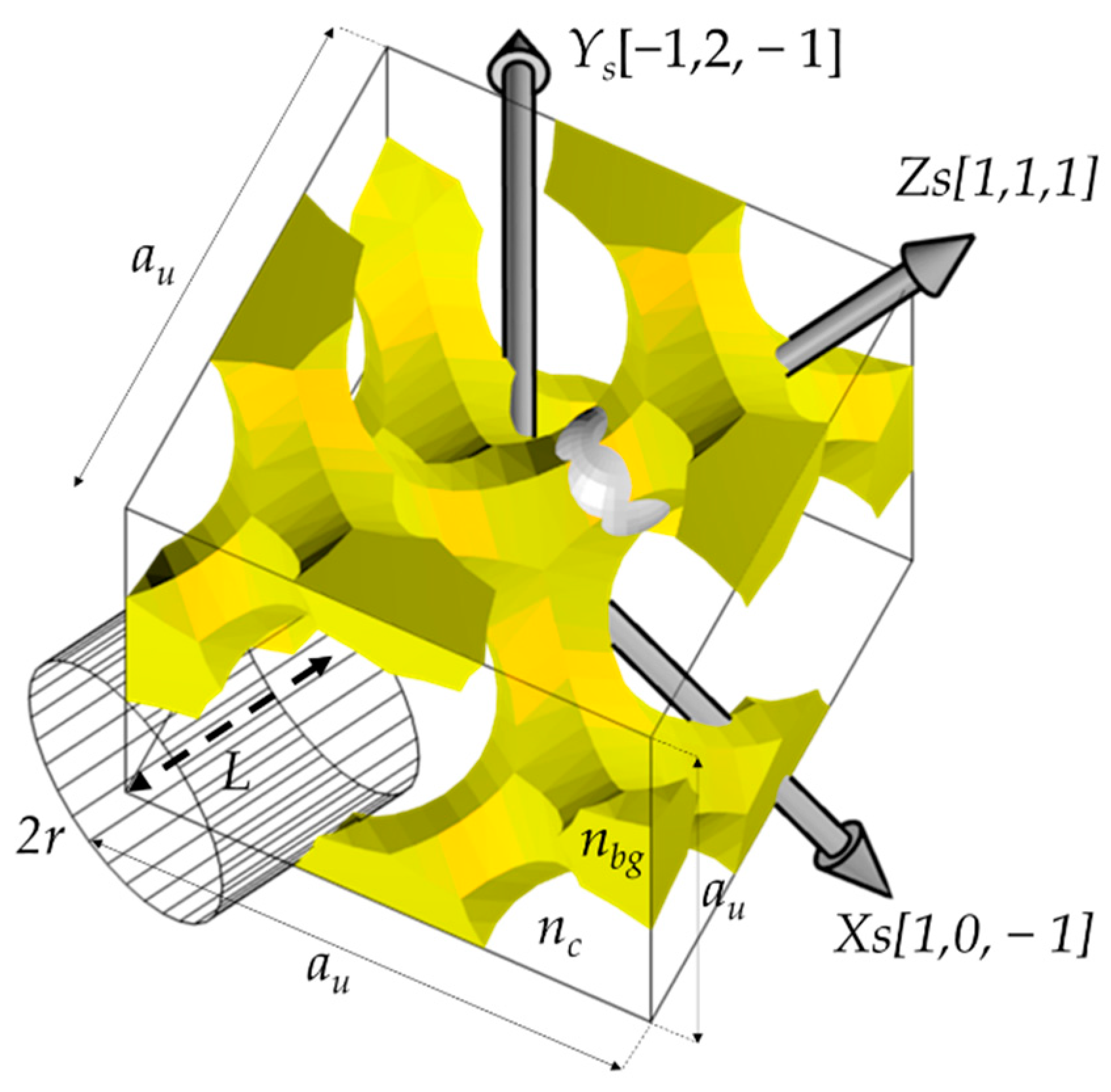
2. Numerical Modeling and Calculation Method
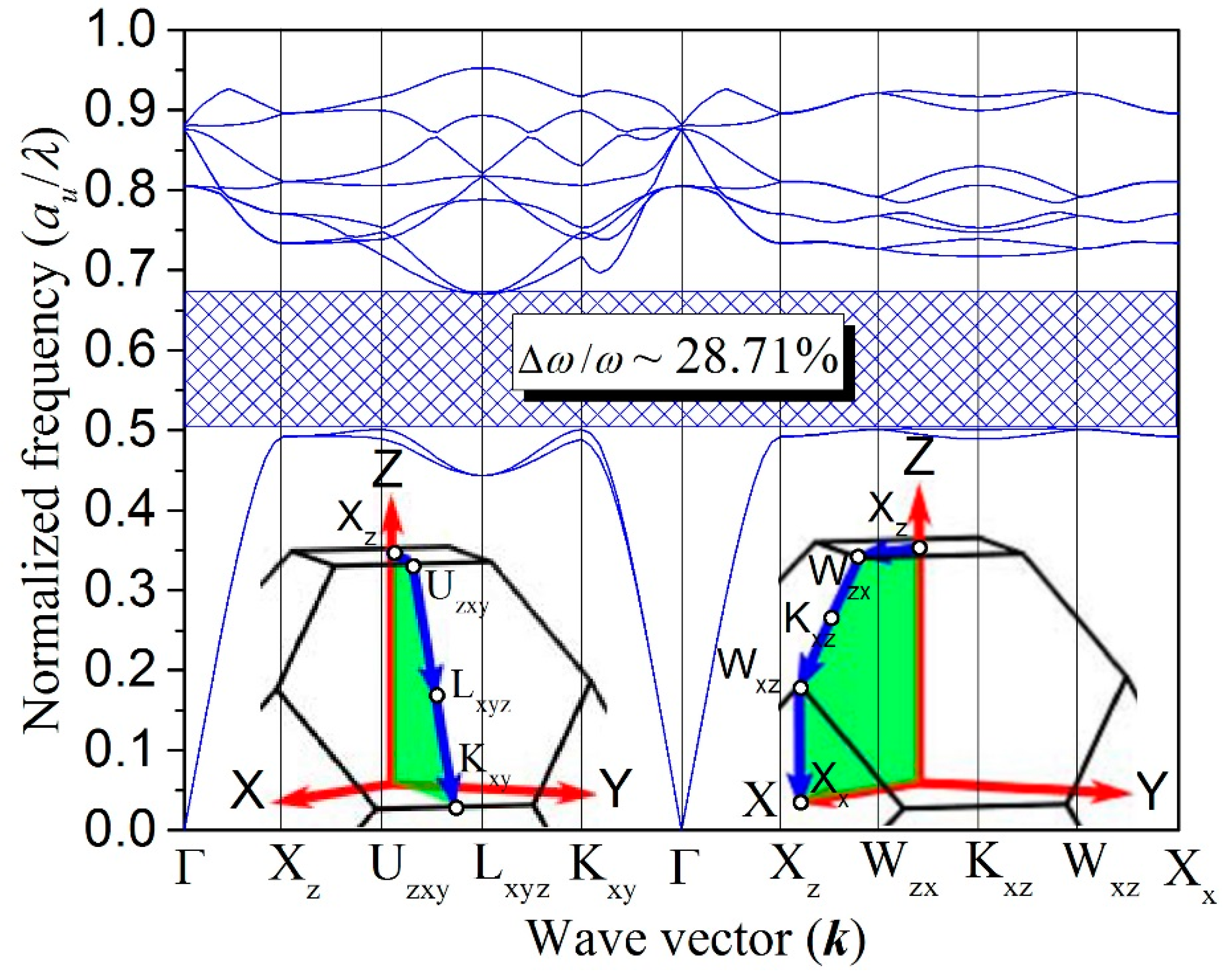
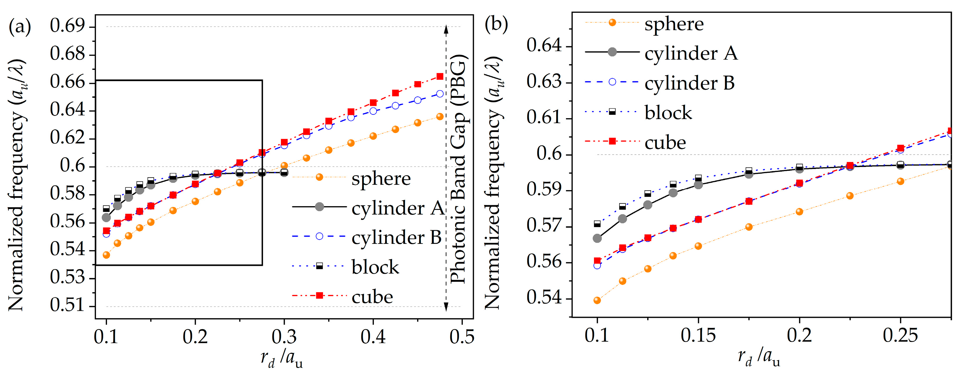
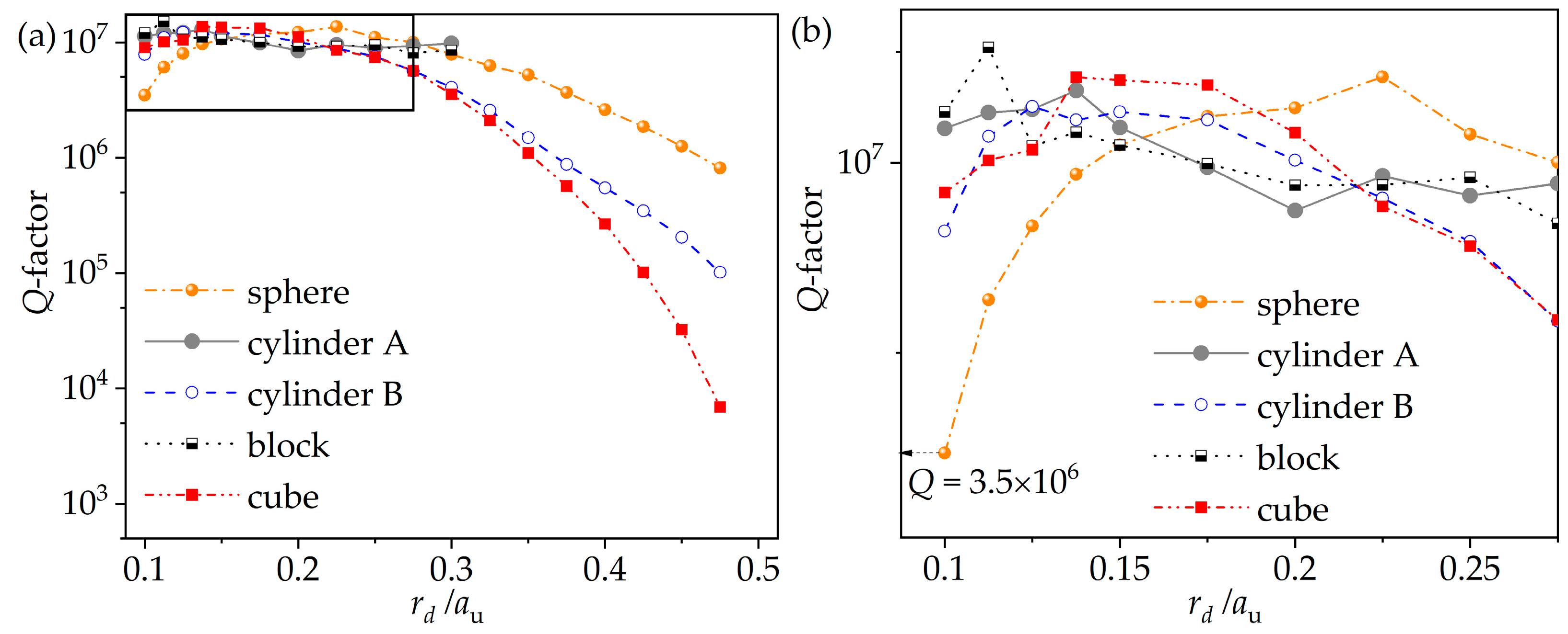
For this paper, we studied high-refractive-index contrast (3.6:1 (GaAs or Si-air)) 3D photonic crystals (PhC) with an inverse RCD lattice structure (air-rods in high-index background material). The corresponding cubic unit-cell (of size au) is shown in Figure 1, along with the defect position. We optimized the relative air-rod radius (r/au) of the inverse RCD structures to maximize their full PBG for an index contrast of nbg:nc = 3.6:1, by evaluating the relative gap width between bands 2 and 3 as a function of the normalized rod radius, r/au. The results are shown in Figure 2. An optimal radius of rIRCD = 0.27au was found, with a corresponding maximum PBG of Δω/ω0~28.71%. This radius is similar to, although slightly larger than, the one found previously (rIRCD/au = 0.26) for an index contrast of 3.3:1 [19]. Figure 3 shows the band structure corresponding to the optimal radius. The maximum PBG goes from au~0.51 to 0.69 with a mid-gap frequency of au/λ~0.6. The optimal radius of the air-rod, r, is about 2.7 times larger than that in the direct RCD scenario, making manufacturing more feasible [19].
Here, the finite inverse RCD structures used for the FDTD simulations were created by truncating an infinite crystal, using a cube with a size of 10au × 10au × 10au, centered on the defect, as previously performed by [19] for high-index defects. The grey axes shown in Figure 1 correspond to the basis used in the FDTD simulations, which was chosen so that the simulation Z-axis (Zs) is along the [1,1,1] axis of the conventional cubic unit-cell, aligned with the inverse rod going through the defects [19]. All the simulations used the same inverse RCD crystal, with cylinders of radius r = 0.27au and with refractive indices of nc = 1.0 for the cylinders and nbg = 3.6 for the background (see Figure 1). The dimensions of the defects and the various shapes are detailed in Figure 4. Five different defect types were considered: (a) a sphere of radius, rd, (b) a cylinder (“cylinder A”) of fixed height L = 3 a u / 4 , with a circular base of diameter D = 2rd, (c) a cylinder (“cylinder B”) of height LcylB = 2rd equal to its diameter D = 2rd, (d) a block of fixed height L = 3 a u / 4 , with a square base of side-length W = 2rd, and (e) a cube of side-length Wcube = Lcube = 2rd. A wide range of defect forms has been chosen to investigate the sensitivity of the resonance modes to the cavity shape, which will be affected by fabrication limitations. For the defects “sphere”, “cylinder B” and “cube”, the size along the axis Zs keeps increasing, while for “cylinder B” and “block”, it is restricted, leading to a maximum rd value past which there are no more effects (until the defect starts cutting into other inverse RCD rods).
All defects have a refractive index of air ndef = 1.0. For each defect type, the FDTD simulations were run using a broadband dipole source, which was placed in the optimized location, S2.0 [19], within the crystal along the Γ-L or [1,1,1] axis. While the refractive index value used in [19] was nbg = 3.3, instead of the nbg = 3.6 used here, we assume that the field distributions would be similar for equivalent geometries and, therefore, that S2.0 would still be an optimal defect location for the background index used here. The dipole was excited along the [1,1,1] axis (Zs direction).

3. Results

After calculating the amplitude of the electric field over time for an inverse RCD with these defects, the Q-factors (Q = λresλ) can then be estimated by analyzing the resulting field decay in the frequency domain, via the fast Fourier transform (FFT) algorithm. Any perturbation disrupting the translational symmetry can act as a defect. Hence, precise tuning of the cavity resonances can be achieved by varying the amount of perturbation, through the modification of defect shapes and sizes in the 3D PhCs. We varied the size of rd from 0.1au to 0.15au in 0.0125au steps and 0.15au to 0.5au in 0.025au steps. Figure 5 shows the normalized frequency of resonance peaks (au/λ) as a function of the normalized size (rd/au), within a full PBG between au/λ~0.51 and 0.69 (mid-gap frequency au/λ~0.6). The normalized resonance frequency (au/λ) of the defect cavities increases with the defect size, except in the case of the cylinder and rectangular block defect cavities.
The corresponding Q-factors obtained for the different defect types are shown in Figure 6. They decrease with increasing defect size. Overall, the Q-factors of the various defect types behave similarly.
The appropriate selection of the shape and size of defects is critical for optimizing the confinement of the electric field within the cavities. Having determined the resonant frequency, a cavity mode on resonance can be visualized using a single frequency snapshot. The resulting normalized square of the electric field distribution (|E|2/|E|2max) for each defect type is illustrated in Figure 7, in the case of rd = 0.1au.
The isosurfaces of the dielectric material and the normalized square of the electric field distributions (using an isovalue of |E|2/|E|2max = 0.03) around the defect regions are shown in Figure 7a,c,e, while the corresponding 1D cross-section plots along the Xs, Ys, Zs axes, going through the defect centers, are shown in Figure 7b,d,f. As the truncated shape of the cavity varies, the |E|2/|E|2max no longer resembles the original electric field mode (i.e., Gaussian modulated sinusoidal mode) with a discontinuity, but instead becomes more confined to either edge of the high-index material.
Observation of modified spontaneous emission and non-linear optical effects in microcavities depend on their high-quality factors (Q) and small mode volumes (Veff), that is, a high ratio of Q/Veff. However, in most optical systems, there is a tradeoff between achieving a higher Q and reducing the size of the cavity mode volume. Here, we compare the mode volumes for different sizes and shapes of defect cavities within the finite inverse RCD structures. An effective mode volume (Veff) of the cavity modes can be calculated from FDTD simulation results, via the definition of the effective mode volume, Veff, and the dimensionless normalized mode volume, fopt [32,33,34]:
    V e f f =   ε ( r ) | E ( r ) | 2 d 3 r ε ( r max ) [ | E ( r ) | 2 ] max
f o p t = V e f f [ λ / n ( r max ) ] 3
where rmax is the position of the maximum electric-field amplitude. Hence, the mode volume can be minimized by increasing the mode maximum electric field and localizing the mode maximum in the low index region.
The results obtained using Equations (1) and (2) are shown in Figure 8. The mode volumes of sphere defects are smaller than in any other shape. In general, the mode volumes decrease with decreasing defect sizes, as expected, except for some small reverses at rd = 0.1375au and 0.275au. For an air sphere (rd = 0.1au), a mode volume down to Veff~0.0022(λ/n)3 and a Q-factor up to ~3.5 × 10⁶ can be achieved (normalized resonance frequency au/λ~0.541). Moreover, because the bandgap is omnidirectional, it is possible to further increase the Q-factor by simply increasing the number of periods in each direction, while maintaining a small mode volume, Veff.

4. Discussion and Conclusions

For this research, inverse RCD PhCs formed in high-index-contrast materials (3.6:1.0 (GaAs:air)) were considered. A maximum PBG of ~28.71% at (r/au)opt = 0.27 was found, using the PWE method. Various defect cavities of varying sizes and shapes, placed in an optimized location within the inverse RCD structures, were studied. The Q-factors and mode volumes (Veff) were calculated, using the FDTD method. In this paper, we report that an air sphere defect (rd = 0.1au) gives the best result, with a mode volume Veff~0.0022 (λres/nair)3 and Q~3.5 × 10⁶, which corresponds to a Q/Veff ratio ~1.59 × 10⁹ (λres/nair)−3 with a resonance at au/λ~0.541. To our knowledge, this is a record-low mode volume for defect cavities in 3D photonic crystal structures. This is, at first sight, a surprising result, given the physical volume of these defects. However, the small mode volume reflects the highly peaked fields close to the high-index cavity edges. Better control of the peak field could be obtained by engineering spikes of high-index material close to the cavity center, similar to recent 2D “bow-tie” cavity designs [10].
Such high-Q cavities with ultra-small mode volume could demonstrate a universal mechanism for broad bandwidth, lossless, wavelength-scale optical circuits in a fully 3D photonic crystal microchip. Additionally, these microchips could allow the development of ultrasensitive sensing chips (guiding and confining light in air or low refractive-index materials) [35] and find applications in solar energy trapping and harvesting [36].

Author Contributions

Conceptualization, Y.-L.D.H. and J.G.R.; formal analysis, Y.-L.D.H. and M.P.C.T.; investigation, Y.-L.D.H. and M.P.C.T.; data curation, Y.-L.D.H. and M.P.C.T.; writing—original draft preparation, Y.-L.D.H. and M.P.C.T.; writing—review and editing, M.P.C.T., Y.-L.D.H. and J.G.R.; supervision, Y.-L.D.H. and J.G.R.; project administration, Y.-L.D.H. and J.G.R.; funding acquisition, Y.-L.D.H. and J.G.R. All authors have read and agreed to the published version of the manuscript.

Funding

This research was funded by the Engineering and Physical Sciences Research Council (EPSRC), grant number EP/V040030/1, EP/M009033/1 and EP/M024458/1.

Institutional Review Board Statement

Not applicable.

Informed Consent Statement

Not applicable.

Data Availability Statement

Not applicable.

Acknowledgments

This work was carried out using the computational facilities of the Advanced Computing Research Center, University of Bristol—http://www.bris.ac.uk/acrc/ (Accessed: 21 February 2022).

Conflicts of Interest

The authors declare no conflict of interest.

References

  1. Yablonovitch, E. Inhibited Spontaneous Emission in Solid-State Physics and Electronics. Phys. Rev. Lett. 1987, 58, 2059–2062. [Google Scholar] [CrossRef] [PubMed] [Green Version]
  2. John, S. Strong Localization of Photons in Certain Disordered Dielectric Superlattices. Phys. Rev. Lett. 1987, 58, 2486–2489. [Google Scholar] [CrossRef] [Green Version]
  3. Joannopoulos, J.D.; Johnson, S.G.; Winn, J.N.; Meade, R.D. Photonic Crystals: Molding the Flow of Light, 2nd ed.; Princeton University Press: Princeton, NJ, USA, 2008. [Google Scholar]
  4. Purcell, E.M. Spontaneous Emission Probabilities at Radio Frequencies. Phys. Rev. 1946, 69, 246–260. [Google Scholar] [CrossRef]
  5. Khitrova, G.; Gibbs, H.M.; Kira, M.; Koch, S.W.; Scherer, A. Vacuum Rabi Splitting in Semiconductors. Nat. Phys. 2006, 2, 81–90. [Google Scholar] [CrossRef]
  6. Vos, W.L.; Woldering, L.A. Cavity Quantum Electrodynamics with Three-Dimensional Photonic Bandgap Crystals. In Light Localisation and Lasing: Random and Quasi-Random Photonic Structures; Ghulinyan, M., Pavesi, L., Eds.; Cambridge University Press: Cambridge, UK, 2015; pp. 180–213. [Google Scholar]
  7. Reiserer, A.; Rempe, G. Cavity-Based Quantum Networks with Single Atoms and Optical Photons. Rev. Mod. Phys. 2015, 87, 1379–1418. [Google Scholar] [CrossRef]
  8. Pandey, S.; Baburaj, N.; Joseph, S.; Joseph, J. Resonant Optical Modes in Periodic Nanostructures. ISSS J. Micro Smart Syst. 2022. [Google Scholar] [CrossRef]
  9. Gowdhami, D.; Balaji, V.R.; Murugan, M.; Robinson, S.; Hegde, G. Photonic Crystal Based Biosensors: An Overview. ISSS J. Micro Smart Syst. 2022. [Google Scholar] [CrossRef]
  10. Hu, S.; Khater, M.; Salas-Montiel, R.; Kratschmer, E.; Engelmann, S.; Green, W.M.J.; Weiss, S.M. Experimental Realization of Deep-Subwavelength Confinement in Dielectric Optical Resonators. Sci. Adv. 2018, 4, eaat2355. [Google Scholar] [CrossRef] [Green Version]
  11. von Freymann, G.; Ledermann, A.; Thiel, M.; Staude, I.; Essig, S.; Busch, K.; Wegener, M. Three-Dimensional Nanostructures for Photonics. Adv. Funct. Mater. 2010, 20, 1038–1052. [Google Scholar] [CrossRef]
  12. Chen, L.; Morgan, K.A.; Alzaidy, G.A.; Huang, C.-C.; Ho, Y.-L.D.; Taverne, M.P.C.; Zheng, X.; Ren, Z.; Feng, Z.; Zeimpekis, I.; et al. Observation of Complete Photonic Bandgap in Low Refractive Index Contrast Inverse Rod-Connected Diamond Structured Chalcogenides. ACS Photonics 2019, 6, 1248–1254. [Google Scholar] [CrossRef] [Green Version]
  13. Fushman, I.; Englund, D.; Vučković, J. Coupling of PbS Quantum Dots to Photonic Crystal Cavities at Room Temperature. Appl. Phys. Lett. 2005, 87, 241102. [Google Scholar] [CrossRef] [Green Version]
  14. Miura, R.; Imamura, S.; Ohta, R.; Ishii, A.; Liu, X.; Shimada, T.; Iwamoto, S.; Arakawa, Y.; Kato, Y.K. Ultralow Mode-Volume Photonic Crystal Nanobeam Cavities for High-Efficiency Coupling to Individual Carbon Nanotube Emitters. Nat. Commun. 2014, 5, 5580. [Google Scholar] [CrossRef] [PubMed] [Green Version]
  15. Aharonovich, I.; Englund, D.; Toth, M. Solid-State Single-Photon Emitters. Nat. Photonics 2016, 10, 631–641. [Google Scholar] [CrossRef]
  16. Alam, M.W.; Souayeh, B.; Islam, S.F. Enhancement of Thermoelectric Performance of a Nanoribbon Made of α-T3 Lattice. J. Phys. Condens. Matter 2019, 31, 485303. [Google Scholar] [CrossRef] [Green Version]
  17. Taverne, M.P.C.; Ho, Y.-L.D.; Zheng, X.; Chen, L.; Fang, C.-H.N.; Rarity, J. Strong Light Confinement in Rod-Connected Diamond Photonic Crystals. Opt. Lett. 2018, 43, 5202–5205. [Google Scholar] [CrossRef] [PubMed]
  18. Zheng, X.; Taverne, M.; Ho, Y.-L.; Rarity, J. Cavity Design in Woodpile Based 3D Photonic Crystals. Appl. Sci. 2018, 8, 1087. [Google Scholar] [CrossRef] [Green Version]
  19. Taverne, M.P.C.; Ho, Y.-L.D.; Zheng, X.; Liu, S.; Chen, L.-F.; Lopez-Garcia, M.; Rarity, J.G. Modelling Defect Cavities Formed in Inverse Three-Dimensional Rod-Connected Diamond Photonic Crystals. EPL (Europhys. Lett.) 2016, 116, 64007. [Google Scholar] [CrossRef] [Green Version]
  20. Taverne, M.P.C.; Ho, Y.-L.D.; Rarity, J.G. Investigation of Defect Cavities Formed in Three-Dimensional Woodpile Photonic Crystals. J. Opt. Soc. Am. B 2015, 32, 639. [Google Scholar] [CrossRef] [Green Version]
  21. Ho, Y.D.; Ivanov, P.S.; Engin, E.; Nicol, M.F.J.; Taverne, M.P.C.; Chengyong, H.; Cryan, M.J.; Craddock, I.J.; Railton, C.J.; Rarity, J.G. FDTD Simulation of Inverse 3-D Face-Centered Cubic Photonic Crystal Cavities. IEEE J. Quantum Electron. 2011, 47, 1480–1492. [Google Scholar] [CrossRef]
  22. Wang, C.; Quan, Q.; Kita, S.; Li, Y.; Lončar, M. Single-Nanoparticle Detection with Slot-Mode Photonic Crystal Cavities. Appl. Phys. Lett. 2015, 106, 261105. [Google Scholar] [CrossRef] [Green Version]
  23. Liang, F.; Quan, Q. Detecting Single Gold Nanoparticles (1.8 Nm) with Ultrahigh- Q Air-Mode Photonic Crystal Nanobeam Cavities. ACS Photonics 2015, 2, 1692–1697. [Google Scholar] [CrossRef]
  24. Ryckman, J.D.; Weiss, S.M. Low Mode Volume Slotted Photonic Crystal Single Nanobeam Cavity. Appl. Phys. Lett. 2012, 101, 071104. [Google Scholar] [CrossRef] [Green Version]
  25. Chan, C.T.; Datta, S.; Ho, K.M.; Soukoulis, C.M. A 7 Structure: A Family of Photonic Crystals. Phys. Rev. B 1994, 50, 1988–1991. [Google Scholar] [CrossRef] [PubMed] [Green Version]
  26. Maldovan, M.; Thomas, E.L. Diamond-Structured Photonic Crystals. Nat. Mater. 2004, 3, 593–600. [Google Scholar] [CrossRef] [PubMed]
  27. Sellers, S.R.; Man, W.; Sahba, S.; Florescu, M. Local Self-Uniformity in Photonic Networks. Nat. Commun. 2017, 8, 14439. [Google Scholar] [CrossRef] [PubMed] [Green Version]
  28. Edagawa, K. Photonic Crystals, Amorphous Materials, and Quasicrystals. Sci. Technol. Adv. Mater. 2014, 15, 34805. [Google Scholar] [CrossRef] [PubMed] [Green Version]
  29. Men, H.; Lee, K.Y.K.; Freund, R.M.; Peraire, J.; Johnson, S.G. Robust Topology Optimization of Three-Dimensional Photonic-Crystal Band-Gap Structures. Opt. Express 2014, 22, 22632. [Google Scholar] [CrossRef] [Green Version]
  30. Johnson, S.; Joannopoulos, J. Block-Iterative Frequency-Domain Methods for Maxwell’s Equations in a Planewave Basis. Opt. Express 2001, 8, 173. [Google Scholar] [CrossRef] [Green Version]
  31. Railton, C.J.; Hilton, G.S. The Analysis of Medium-Sized Arrays of Complex Elements Using a Combination of FDTD and Reaction Matching. IEEE Trans. Antennas Propag. 1999, 47, 707–714. [Google Scholar] [CrossRef] [Green Version]
  32. Coccioli, R.; Boroditsky, M.; Kim, K.W.; Rahmat-Samii, Y.; Yablonovitch, E. Smallest Possible Electromagnetic Mode Volume in a Dielectric Cavity. IEE Proc. Optoelectron. 1998, 145, 391–397. [Google Scholar] [CrossRef]
  33. Boroditsky, M.; Vrijen, R.; Krauss, T.F.; Coccioli, R.; Bhat, R.; Yablonovitch, E. Spontaneous Emission Extraction and Purcell Enhancement from Thin-Film 2-D Photonic Crystals. J. Light. Technol. 1999, 17, 2096–2112. [Google Scholar] [CrossRef] [Green Version]
  34. Yu, P.; Qi, B.; Jiang, X.; Wang, M.; Yang, J. Ultrasmall-V High-Q Photonic Crystal Nanobeam Microcavities Based on Slot and Hollow-Core Waveguides. Opt. Lett. 2011, 36, 1314. [Google Scholar] [CrossRef] [PubMed]
  35. Yoshie, T.; Tang, L.; Su, S.-Y. Optical Microcavity: Sensing down to Single Molecules and Atoms. Sensors 2011, 11, 1972–1991. [Google Scholar] [CrossRef] [PubMed]
  36. John, S. Why Trap Light? Nat. Mater. 2012, 11, 997–999. [Google Scholar] [CrossRef] [PubMed]
Figure 1. The cubic unit-cell of the inverse RCD structure (yellow = high refractive index, nbg) with the dimension au. One of the large air rods, with a refractive index nc = 1, radius r = 0.27au and height L = 3 a u / 4 , used to create the inverse RCD structure, is shown as a black wireframe cylinder. The grey sphere indicates the position of the studied defects. The lattice directions corresponding to our simulation axes Xs, Ys, and Zs are shown as grey arrows.
Crystals 12 00303 g001
Figure 2. Gap-width to center-frequency ratio Δω/ω0 (between band 2 and band 3), as a function of the normalized rod radius r/au for inverse RCD structures at a refractive index contrast of nbg:nc = 3.6:1. It shows a maximal gap width of Δω/ω0 = 28.71% for r/au = 0.27.
Crystals 12 00303 g002
Figure 3. Bandgap diagram of the optimal inverse RCD (r = 0.27 au). The inset graphs show the movement described by the wave vector along the surface of the first Brillouin zone, in the corresponding left and right parts of the plot.
Crystals 12 00303 g003
Figure 4. Five types of defect shapes including (a) a sphere of diameter D = 2rd, (b) a cylinder (“cylinder A”) of diameter D = 2rd and height L = 3 a u / 4 , (c) a cylinder (“cylinder B”) of diameter D = 2rd and height of LcylB = 2rd, (d) a rectangular block with a square base of side length W = 2rd and a height of L = 3 a u / 4 , (e) a cube of side length Wcube = Lcube = 2rd. The size of the defects varied from rd = 0.1au to 0.15au in 0.0125au steps and 0.15au to 0.5au in 0.025au steps. Here, the studied low-index-filled cavities (ndef = 1.0) are placed in the optimized location, S2.0 [19], within the crystal along the Γ-L or Zs [1,1,1] axis.
Crystals 12 00303 g004
Figure 5. The normalized frequency of resonance peaks (au/λ), as a function of the normalized radii (rd/au). The dashed lines indicate the limits of the full bandgap from au/λ~0.506 to 0.694 and its mid-gap frequency au/λ~0.600. (b) Zoom-in of the highlighted region in (a).
Crystals 12 00303 g005
Figure 6. (a) Q-factors obtained for the various normalized radii (rd/au) and defect types. (b) Zoom-in of the highlighted region in (a).
Crystals 12 00303 g006
Figure 7. Isosurfaces of the material (red), and of the normalized square of the electric field distributions for |E|2/|E|2max = 0.03 (yellow) with embedded low-index (ndef = 1.0) truncated regions of various defect shapes (in the case of rd = 0.1au): a sphere (a1f1), cylinder A (a2f2), cylinder B (a3f3), a block (a4f4) and a cube (a5f5). The cavities were excited by a dipole with an electric field oriented along the Zs directions, using a short Gaussian pulse. The solid lines show the center of the defect and the dashed lines show the position of the maximum electric-field value. (b1b5,d1d5,f1f5): one-dimensional cross-section plots of the normalized square of the electric field (|E|2/|E|2max) created along the Xs, Ys, and Zs axes, and going through the maxima of each field distribution (dashed lines on the 3D isosurface plots).
Crystals 12 00303 g007
Figure 8. Normalized mode volumes, obtained for the various normalized radii (rd/au) and defect types. (b) Zoom-in of the highlighted region in (a).
Crystals 12 00303 g008
Publisher’s Note: MDPI stays neutral with regard to jurisdictional claims in published maps and institutional affiliations.

