Abstract
High-efficiency and stable hole transport materials (HTMs) play an essential role in high-performance planar perovskite solar cells (PSCs). 2,2,7,7-tetrakis(N,N-di-p-methoxyphenylamine)-9,9-spirobi-fluorene (Spiro-OMeTAD) is often used as HTMs in perovskite solar cells because of its excellent characteristics, such as energy level matching with perovskite, good film-forming ability, and high solubility. However, the accumulation and hydrolysis of the common additive Li-TFSI in Spiro-OMeTAD can cause voids/pinholes in the hole transport layer (HTL), which reduces the efficiency of the PSCs. In order to improve the functional characteristics of HTMs, in this work, we first used CsI as a dopant to modify the HTL and reduce the voids in the HTL. A small amount of CsI is introduced into Spiro-OMeTAD together with Li-TFSI and 4-tert-butylpyridine (TBP). It is found that CsI and TBP formed a complex, which prevented the rapid evaporation of TBP and eliminated some cracks in Spiro-OMeTAD. Moreover, the uniformly dispersed TBP inhibits the agglomeration of Li-TFSI in Spiro-OMeTAD, so that the effective oxidation reaction between Spiro-OMeTAD and air produces Spiro-OMeTAD+ in the oxidation state, thereby increasing the conductivity and adjusting the HTL energy. Correspondingly, the PCE of the planar PSC of the CsI-modified Spiro-OMeTAD is up to 13.31%. In contrast, the PSC without CsI modification showed a poor PCE of 10.01%. More importantly, the PSC of Spiro-OMeTAD treated with CsI has negligible hysteresis and excellent long-term stability. Our work provides a low-cost, simple, and effective method for improving the performance of hole transport materials and perovskite solar cells.
1. Introduction
Organic-inorganic hybrid perovskite has attracted much attention because of its low exciton binding energy, high absorption coefficient, wide spectral range, and long exciton diffusion length. It is a potential candidate material for next-generation photovoltaic devices [1,2,3,4,5,6]. Organic-inorganic hybrid lead halide perovskite solar cells (PSCs) have the characteristics of good solution processability, low cost, and high energy conversion efficiency [7,8] whicd considered to be a new generation of photovoltaic technology [9,10]. To achieve efficient and stable PSCs, researchers have conducted many explorations, including designing device structures, [11] controlling perovskite film crystallization, regulating the molecular structure of perovskite-type perovskites, and interface engineering. In the typical structure of PSC, the electron transport layer (ETL) and hole transport layer (HTL) play a crucial role in charge extraction and transport and determine the final photovoltaic performance of PSCs. In planar structure PSCs, the perovskite active layer is sandwiched between the hole and electron transport layer to enhance the transport and extraction of photogenerated carriers. In particular, the hole transport layer can facilitate hole extraction and shield anode electrons [12,13,14,15]. Perovskite/HTL interface is also playing a key role in maximizing the photovoltaic performance of PSCs [16,17]. Spiro-OMeTAD is one of the earliest small-molecule hole transport materials used in perovskite cells and is often used as a reference for comparison with newly developed HTMs. The undoped Spiro-OMeTAD has relatively low hole mobility and conductivity, which are in the order of 10−4 cm2 V−1 s−1 and 10−5 S cm−1, respectively [18,19].
The chemical P-type doping strategy has been proved to be an effective method to improve the charge transport capacity of Spiro-OMeTAD [20]. In general, 4-tert-butylpyridine (TBP) and (trifluoromethanesulfonyl)imide (Li-TFSI) are doped in Spiro-OMeTAD to improve the electrical conductivity. Then, Spiro-OMeTAD is oxidized in air to generate more Spiro-OMeTAD+ cation radicals, thus improving the mobility of HTL and regulating the energy level of Spiro-OMeTAD [21,22,23]. Li-TFSI is used as a catalyst to promote the oxidation reaction of Spiro-OMeTAD in air. Another additive (TBP) is used to regulate the solubility of Li-TFSI so that Li-TFSI is evenly distributed in HTL [24]. However, the addition of Li-TFSI and TBP has led to some nasty problems. Li-TFSI is hygroscopic and can easily absorb moisture from the air, which leads to the accumulation of Li-TFSI and reduces the film hole transport performance. Meanwhile, with the gradual evaporation of TBP, some bubbles and voids are left inside HTL, which will further aggravate the accumulation of Li-TFSI, thus inhibiting the charge transmission and collection. Many studies have been proposed to enhance the electrical conductivity and hole mobility of HTL, e.g., cobalt complex (FK209) [25], (SnCl4) [26], perfluoro-tetracyanoquino-dimethane (F4-TCNQ) [27], tetrabutylammonium (TBA) [28] and polymer poly(4-vinylpyridine) (P4VP) [29]. At the same time, it will not only affect the efficiency of the equipment but will also be expensive. Therefore, further efforts to find other HTMs with excellent chemical stability and high hole mobility are necessary to achieve the detector’s high efficiency and long-term stability.
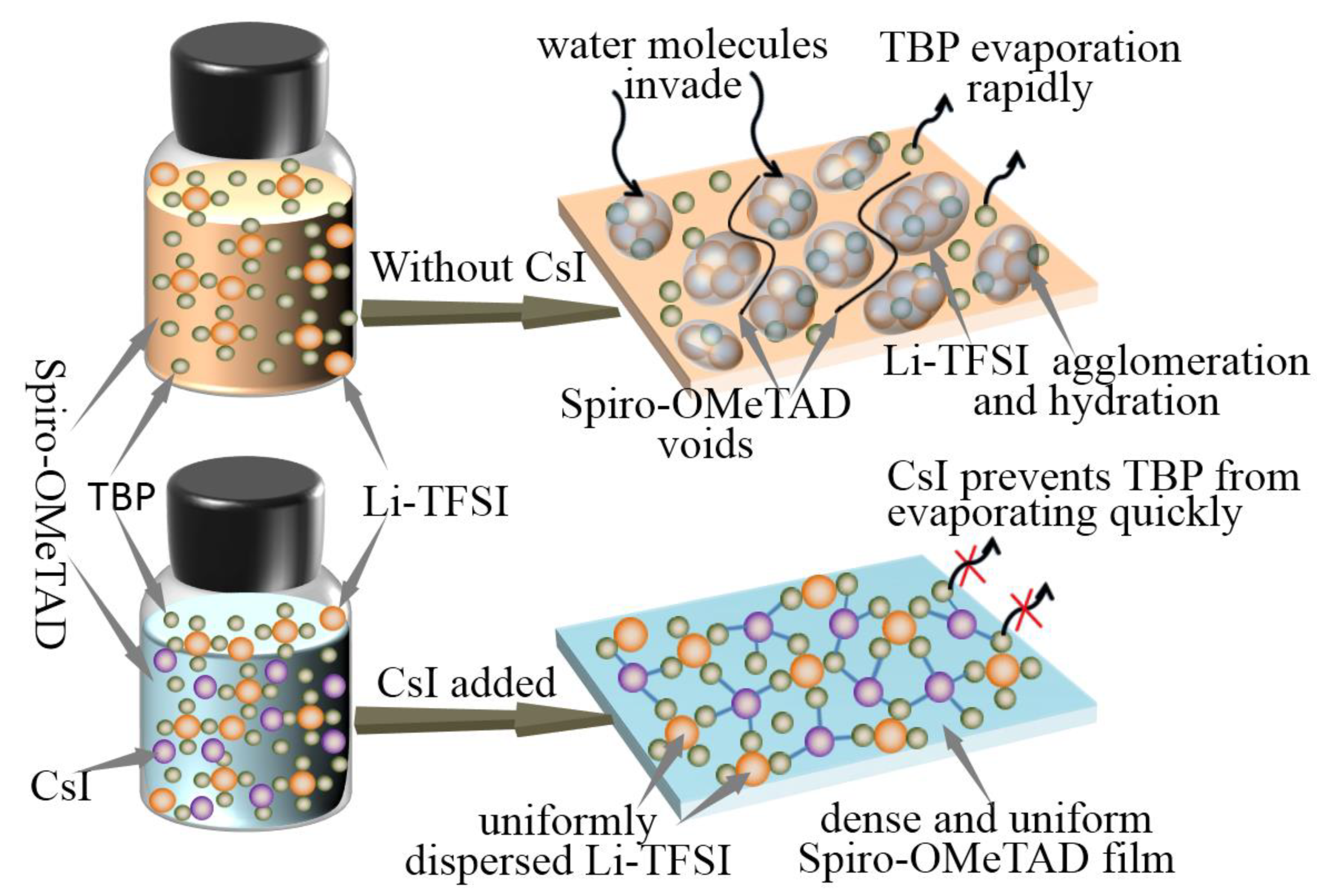
This work uses a simple doped method to develop low-cost HTL doping with high hole mobility and stability. A small amount of CsI is introduced into Spiro-OMeTAD, together with Li-TFSI and TBP as additives. After the study, it is found that CsI and TBP formed a complex, which inhibited the agglomeration of Li-TFSI in Spiro-OMeTAD, thus preventing the rapid evaporation of TBP from leaving some cracks in Spiro-OMeTAD. Compared with Spiro-OMeTAD, which only added Li-TFSI and TBP additives, the Spiro-OMeTAD morphology and hole transport performance are improved after CsI doping. The solar cells made with the optimized Spiro-OMeTAD material showed excellent performance. The results show that due to the improvement of fill factor (FF), short-circuit current density (JSC), and other parameters, the stable output efficiency of PSCs is 13.31%. The CsI and TBP complexes can also inhibit the aggregation and crystallization of Li-TFSI, reducing voids and pinholes. The uniform and dense Spiro-OMeTAD film can effectively avoid moisture infiltration, thereby preventing the decomposition of perovskite.
2. Materials and Methods
Materials: Molybdenum (VI) oxide (MoO3, 99.97%), N, N-dimethylformamide (DMF, 99.8%), Dimethyl sulfoxide (DMSO, ≥99.9%, ACS reagent), bis(trifluoromethane) sulfonamide lithium salt (Li-TFSI), chlorobenzene (CB, 99.9%)and 4-tert-Butylpyridine (TBP, 96%), Acetonitrile (99. 9%, Superdry) are purchased from Sigma-Aldrich. Lead iodide (PbI2, 99.99%) and 2, 2′, 7, 7′-tetrakis (N, N-di-p-methoxyphenylamine)9, 9′-spirobifluorene (Spiro-OMeTAD, 99.8%) are purchased from Xi’an Polymer Light Technology Corp, Xi'an, China. Indium-tin oxide (ITO) transparent conductive film glass and Methylammonium iodide (MAI, ≥99.9%) are purchased from Advanced Election Technology CO.,Ltd, Liaoning, China. Tin (IV) oxide (SnO2), 15% in H2O colloidal dispersion, is purchased from Alfa Aesar, Shanghai, China. All chemicals and solvents are used as received without further purification unless otherwise stated.
Device Fabrication: All PSCs are fabricated on commercial ITO, with patterned glass electrodes less than 10 Ω sq−1. The patterned ITO substrate is thoroughly cleaned in detergent, acetone, 2-propanol, and deionized water for the sequence in an ultrasonic bath for 15 min. Then, the substrate is treated with UV-ozone for 15 min.
SnO2 Film Preparation: SnO2 aqueous solution (15%) is diluted with deionized water at a volume ratio of 1:6. In an air environment, drop the diluted SnO2 solution on the ITO substrate and spin at 4000 rpm for 50 s. Finally, the film is annealed at 150 °C for 30 min. After cooling, the substrates are first treated with UV-ozone for 5 min and transferred into a nitrogen-filled glove box for device fabrication (O2 < 0.01 ppm, H2O < 0.01 ppm).
Perovskite Film Preparation: PbI2 (553.7 mg) and MAI (190.7 mg) are dissolved in N,N-dimethylformamide (DMF, 0.8 mL) and Dimethyl sulfoxide (DMSO, 0.2 mL). The mixtures are kept stirred at 70 °C for one night and filtered through a 0.22 μm filter before use. An amount of 200 µL of 70 °C CH3NH3PbI3 solutions are dispensed onto the SnO2 layer and spin-coated at 3000 rpm for 13 s. The spin speed is then increased to 5000 rpm, and after 5 s, 300 µL of anti-solvent chlorobenzene is dispensed onto the middle of the spinning perovskite film in less than 2 s. Finally, the films are left to spin at 5000 rpm for 50 s. The CH3NH3PbI3 perovskite film spin-coating is done at room temperature (25 °C) and annealed at 100 °C for 15 min.
Spiro-OMeTAD Film Preparation: First, 0.0 wt%, 0.2 wt%, 0.4 wt%, 0.6 wt%, and 0.8 wt% of CsI is dissolved in 1 mL TBP (mass ratio, CsI/TBP), respectively, and then stirred for 30 min (min) to obtain TBP and CsI mixed solution. Then, 72.3 mg of Spiro-OMeTAD is dissolved in 1 mL of chlorobenzene that contains 17.5 µL Li-TFSI (520 mg mL−1 in acetonitrile) and 28.8 µL of the above TBP and CsI mixed solution to obtain Spiro-OMeTAD precursor solution. Then Spiro-OMeTAD precursor solution is spin-coated on perovskite film at 3000 rpm for 40 s and then stored in an air environment (25 %RH and 25 °C) for 8 h.
Finally, molybdenum oxide (≈10 nm) and copper (≈100 nm) are thermally evaporated onto the active layer sequentially under vacuum pressure <10−4 Pa.
3. Results and Discussion
In this study, five types of Spiro-OMeTAD hole transport layer (HTL) are prepared: Spiro-OMeTAD with Li-TFSI, TBP and without CsI (=HTL 0.0 wt%), Spiro-OMeTAD with Li-TFSI, TBP and 0.2 wt% CsI (=HTL 0.2 wt%), Spiro-OMeTAD with Li-TFSI, TBP and 0.4 wt% CsI (=HTL 0.4 wt%), Spiro-OMeTAD with Li-TFSI, TBP and 0.6 wt% CsI(=HTL 0.6 wt%), and Spiro-OMeTAD with Li-TFSI, TBP and 0.8 wt% CsI (=HTL 0.8 wt%). Accordingly, five types of perovskite solar cells (PSC 0.0 wt%, PSC 0.2 wt%, PSC 0.4 wt%, PSC 0.6 wt%, and PSC 0.8 wt%) are manufactured based on the above five HTLs, and their performance is tested. The manufacturing process of PSCs is shown in Figure 1a. First, the electron transport layer (SnO2), photosensitive layer (MAPbI3), and hole transport layer (Spiro-OMeTAD) are gyro-coated on patterned ITO substrates successively.Finally, the device is transferred to a vacuum chamber at 2 × 10⁻⁴ Pa for electrode modified layer (MoO3) evaporation and electrode (Cu). The Experimental Section completely describes the fabrication process of the device. All devices are manufactured under the same conditions, so each layer has the same thickness. As shown in Figure 1b, the device with the ITO/SnO2/MAPbI3/Spiro-OMeTAD (with or without CsI)/MoO3/Cu structure.
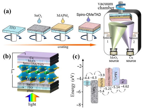
Figure 1.
(a) The manufacturing process of PSCs. (b) The device configuration of PSCs. (c) Energy level diagram of PSCs.
3.1. Spiro-OMeTAD: CsI Films Characterization
Carrier transport in PSCs is closely related to the crystal structure and morphology of HTMs, which affects the performance parameters of the detector [30]. Five types of PSCs are prepared by spin-coating SnO2, organic-inorganic hybrid MAPbI3 layer, and Spiro-OMeTAD (with or without CsI) on ITO coated glass, respectively (Figure 1a,b). The materials have suitable energy level matching, and the energy level diagram of the device is shown in Figure 1c.
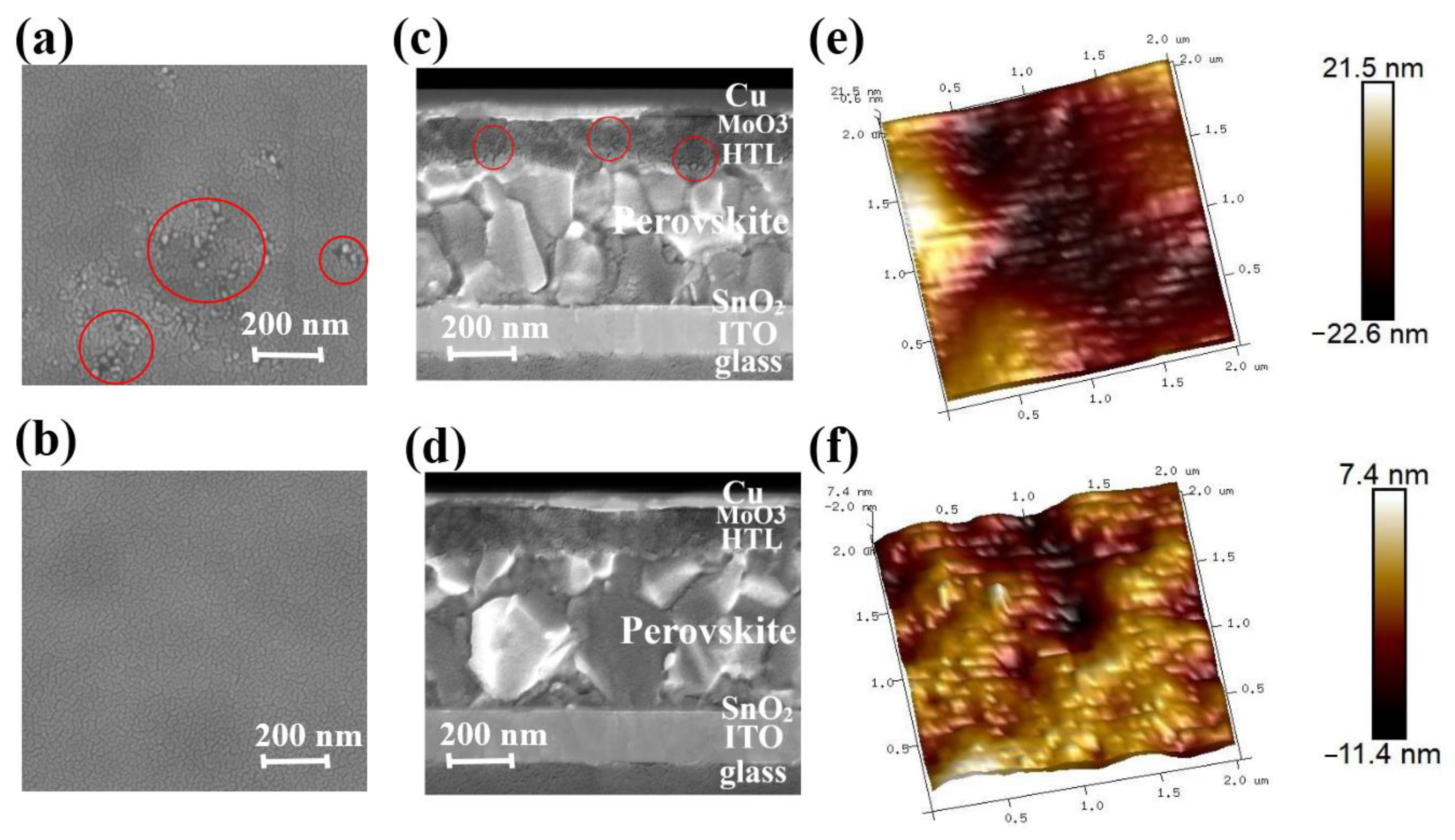
To further investigate the impact of CsI in governing the morphology and microstructure of the HTL, scanning electron microscope (SEM) and atomic force microscopy (AFM) is conducted (Figures S1–S6). Figure S1a–e show the top-view SEM images of fresh Spiro-OMeTAD film (HTL 0.0 wt%, HTL 0.2 wt%, HTL 0.4 wt%, HTL 0.6 wt%, and HTL 0.8 wt%) after spin coating, respectively. As shown in Figure S1a–e, the fresh Spiro-OMeTAD films after spin coating all had a dense and uniform surface. It shows that the addition of CsI will not damage the film-forming properties of Spiro-OMeTAD. In order to improve the hole mobility and conductivity of Spiro-OMeTAD, the spin-coated Spiro-OMeTAD films are oxidized in air. Figure S1f–k shows the top view SEM image of the corresponding Spiro-OMeTAD films after oxidizing in the air for 8 h. As can be seen from Figure 2a and Figure S1f, the Spiro-OMeTAD film that is not optimized by CsI showed obvious aggregation. In contrast, other Spiro-OMeTAD films optimized by CsI remain relatively uniform after oxidation (Figure S1g–k). HTL 0.4 wt% maintains the best uniform and dense film after oxidation (Figure 2b and Figure S1h). Figure 2c shows the SEM image of the cross-sectional view of the device based on HTL 0.0 wt%. There are black aggregates and cracks randomly distributed within the HTL 0.0 wt%, which will seriously hinder the transmission of holes and reduce the device’s performance. In contrast, Figure 2d is a cross-sectional SEM image of a device based on HTL 0.4 wt%, showing a compact multilayer structure with a clear interface. All devices are manufactured under the same conditions, so each functional layer has the same thickness. The thickness of each functional layer of the PSCs can be measured. The cathode electrode (ITO) is about 170 nm, the SnO2 is 20 nm, the perovskite photoactive layer (MAPbI3 or CH3NH3PbI3) is 460 nm, Spiro-OMeTAD is 160 nm, and the copper electrode is 80 nm.

Figure 2.
Top-view SEM images of Spiro-OMeTAD film oxidized at room temperature for 8 h HTL 0.0 wt% (a) and HTL 0.4 wt% (b). Cross-sectional SEM images of PSCs based on HTL 0.0 wt% (c) and HTL 0.4 wt% (d). 3D AFM images of HTL 0.0 wt% (e) and HTL 0.4 wt% (f). Films for the AFM testing in tapping mode. The red circles in panels (a) and (c) represent the aggregated regions of the Spiro-OMeTAD films.
In addition, 3D AFM images confirm that the introduction of CsI significantly improves the films’ morphology (Figure S1i–p). Figure 2e,f show high-resolution AFM images of HTL 0.0 wt% and HTL 0.4 wt%. For the HTL 0.0 wt%, the arithmetic average (Ra) and the root mean square (Rq) are 6.19 nm and 5.13 nm, respectively. On the contrary, when the Spiro-OMeTAD is doped with 0.4 wt% CsI, the film is smooth, Ra is 1.77 nm, and Rq is 2.21 nm. Table S1 shows that with the increase of CsI doped, Ra of Spiro-OMeTAD decreased from 5.13 nm to 1.77 nm (CsI 0.4 wt%), and the Rq decreased from 6.19 nm to 2.21 nm (CsI 0.4 wt%), respectively. When the doping content reaches 0.4 wt%, the minimum surface roughness, in addition, if the doped amount continues to increase, it will lad to the over-precipitation of CsI, resulting in the film’s roughness. Due to the low solubility of CsI in chlorobenzene, CsI crystals will precipitate when TBP solution containing a high concentration of CsI is added to the chlorobenzene solution of Spiro-OMeTAD. The precipitated CsI crystals will increase the roughness of the Spiro-OMeTAD film.
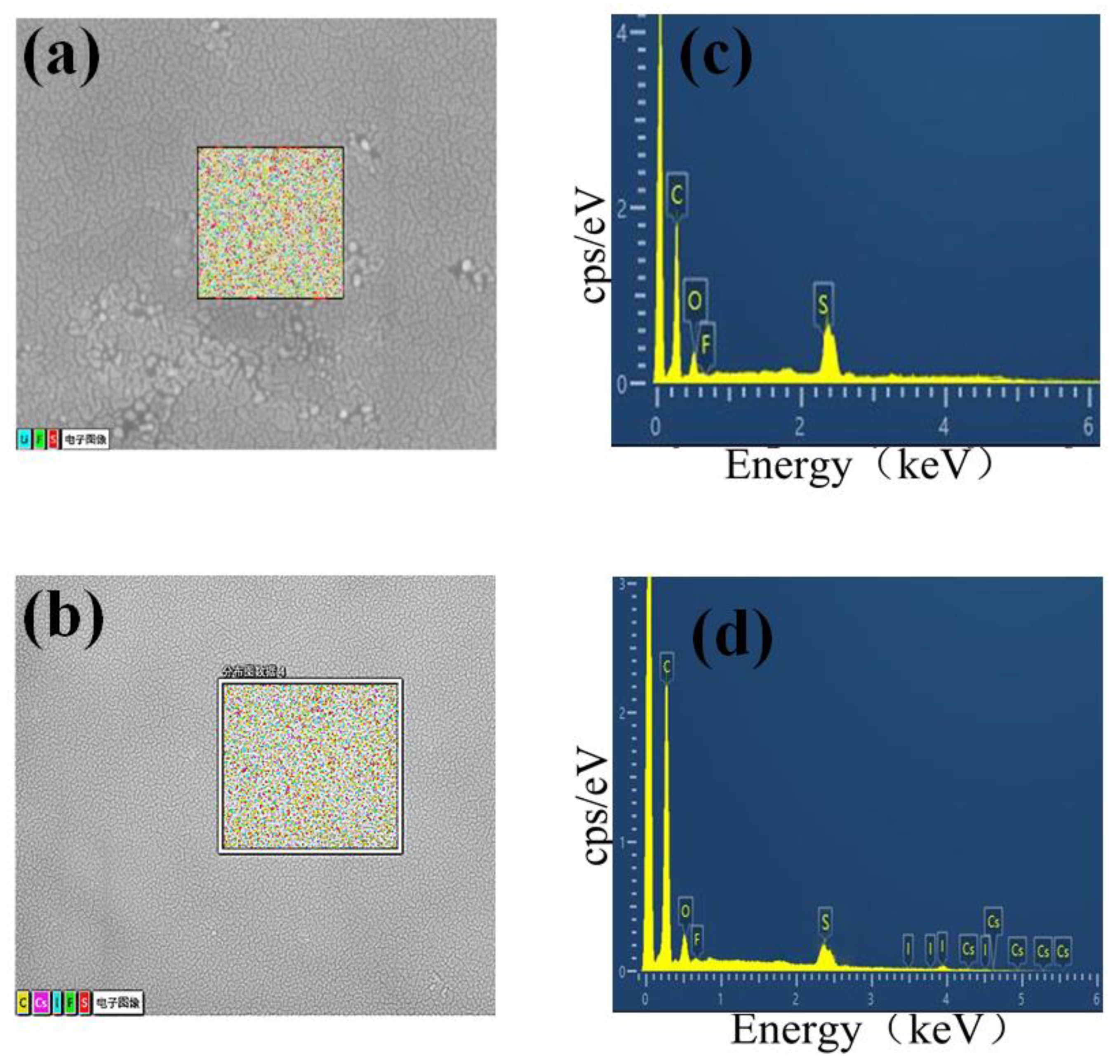
Energy-dispersive X-ray energy spectrum (EDS) analysis of the aggregation centre(Figure 3a,c) revealed the presence of fluorine (F) and sulfur (S), which indicated that Li-TFSI is not uniformly dispersed in the Spiro-OMeTAD, leading to the aggregation of the Spiro-OMeTAD. When 0.4 wt% CsI is added, the Spiro-OMeTAD aggregates disappear and show a uniform surface. EDS could also detect that caesium and iodine elements are evenly dispersed in the Spiro-OMeTAD (Figure 3b,d). These results confirmed that the introduction of CsI prevents the aggregation of Li-TFSI and Spiro-OMeTAD.
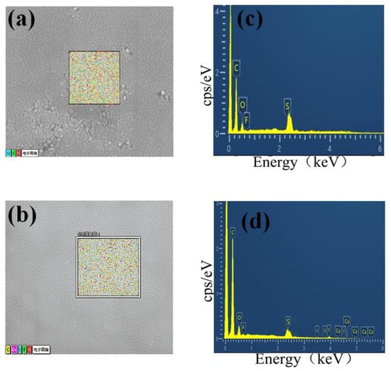
Figure 3.
Energy dispersive X-ray energy spectrum of HTL 0.0 wt% (a,c) and HTL 0.4 wt% (b,d), respectively.
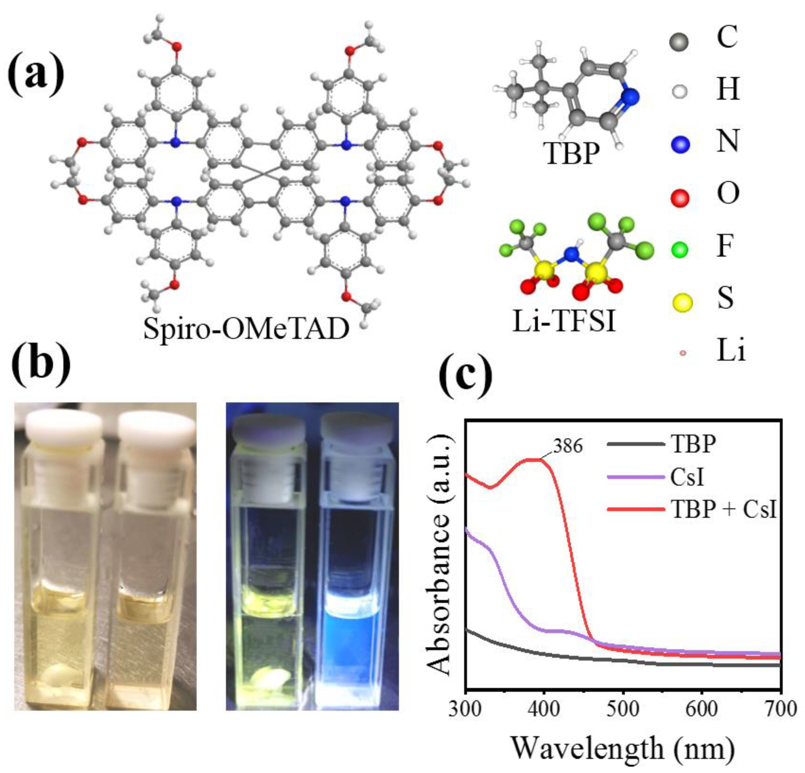
It has been reported that Li-TFSI plays a catalytic role in forming oxidation Spiro-OMeTAD in the ion-doped Spiro-OMeTAD system. Therefore, the uniform distribution of Li-TFSI in HTL can effectively oxidize Spiro-OMeTAD and form more oxidation state Spiro-OMeTAD+, thus improving the hole mobility and overall device performance. In order to determine the interactions in HTL solutions, especially between TBP and CsI, experimental analyses are performed. Under white light, TBP is a yellowish liquid, while under ultraviolet light, TBP emits blue fluorescence. This blue fluorescence disappeared when CsI is added to TBP (Figure 4b). The pure TBP and TBP liquids containing CsI are analyzed by UV-visible spectroscopy. Strong absorption at 386 nm is observed in the absorption spectrum (Figure 4c). These observations indicate an interaction between TBP and CsI molecules. We suspect that CsI introduced into HTL forms a complex of CsI·xTBP that prevents rapid evaporation of TBP. It is well known that the central role of TBP is to disperse Li-TFSI and prevent their agglomeration [24,31]. Figure 5 shows the effect of CsI on preventing Li-TFSI aggregation. When Spiro-OMeTAD containing Li-TFSI and TBP is spin-coated, TBP in the film would evaporate quickly, resulting in Li-TFSI agglomeration. The rapid evaporation of TBP leaves a void inside the HTL, which inhibited charge transfer. The accumulation of Li-TFSI will causes moisture in the air to enter the interior of Spiro-OMeTAD and destroyed its structure easily [32]. CsI·xTBP inhibited the agglomeration Li-TFSI and formed uniform and dense Spiro-OMeTAD film, which effectively inhibited the invasion of moisture. It has been reported that Li-TFSI plays a catalytic role in forming oxidation Spiro-OMeTAD in the ion-doped Spiro-OMeTAD system [33]. Therefore, the uniform distribution of Li-TFSI in HTL can effectively oxidize Spiro-OMeTAD and form more oxidation state Spiro-OMeTAD+, thus improving the hole mobility and overall device performance.
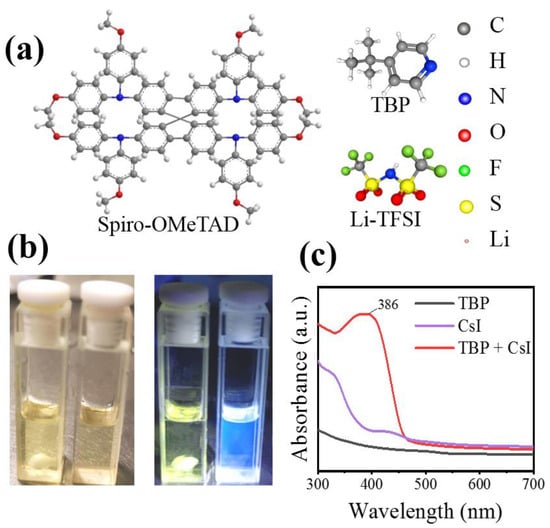
Figure 4.
(a) Molecular structures of Spiro-OMeTAD, Li-TFSI, and TBP. (b) Optical image of TBP and CsI dissolved in TBP under white light (left) and ultraviolet light (right). (c) UV-visible absorption spectra of CsI, TBP, and CsI dissolved in TBP.
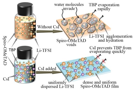
Figure 5.
Schematic illustration of the effect of CsI on preventing Li-TFSI from aggregation.
The water contact angle is measured to investigate the hydrophobicity of Spiro-OMeTAD films further. When 5 microliters of water are placed on the surface of the HTL 0.0 wt%, the water contact angle gradually decreases from 73° to 43° in 2 min (Figure S5a–c). In addition, water gradually penetrates the perovskite layer and hydrolyzes the perovskite in 2 min. In contrast, within 2 min, the contact angle of the Spiro-OMeTAD film treated with 0.4 wt% CsI remained at 81°, and there is no perovskite hydrolysis (Figure S5d). The above experimental results indicate that Spiro-OMeTAD film optimized by 0.4 wt% CsI can inhibit moisture infiltration.
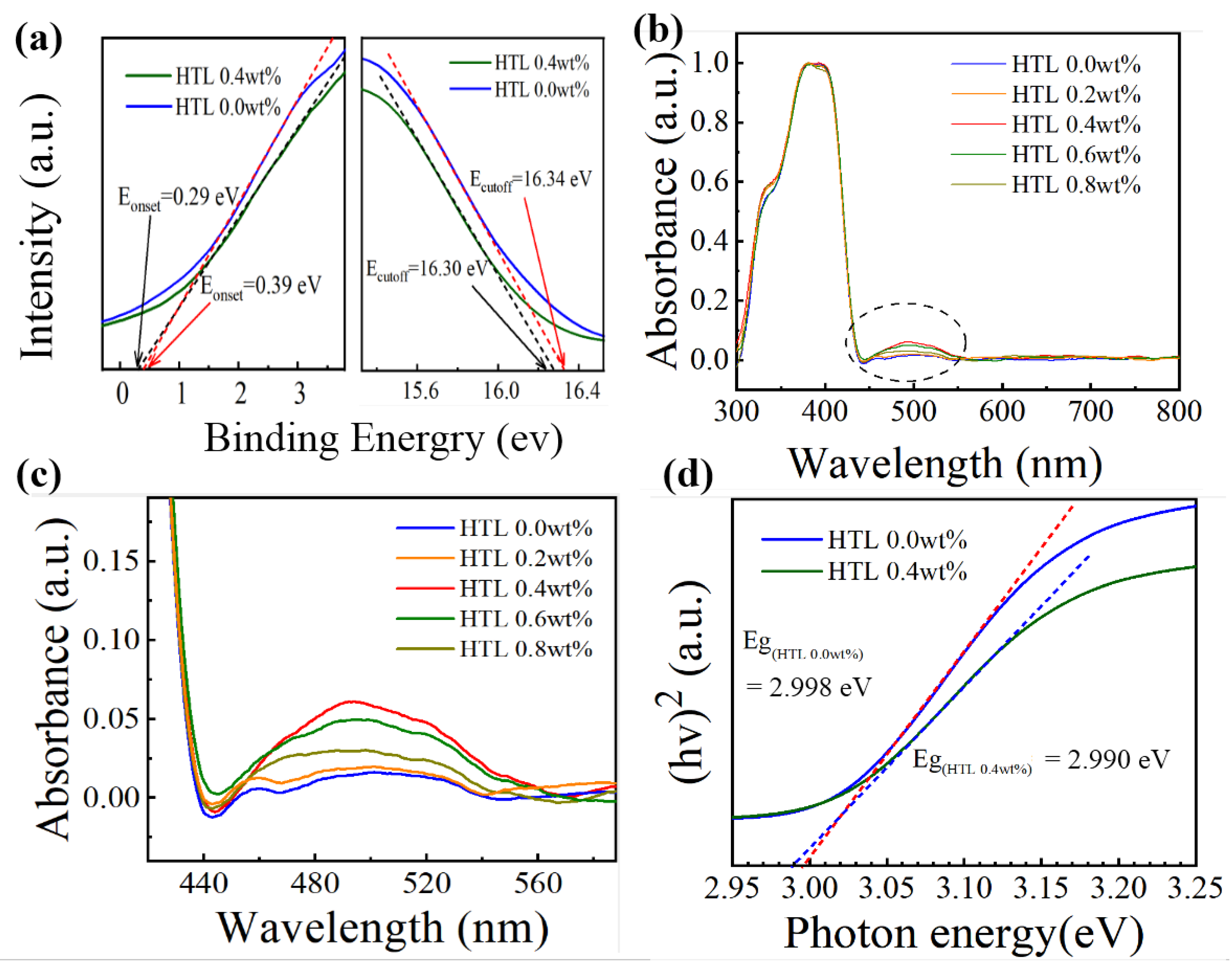
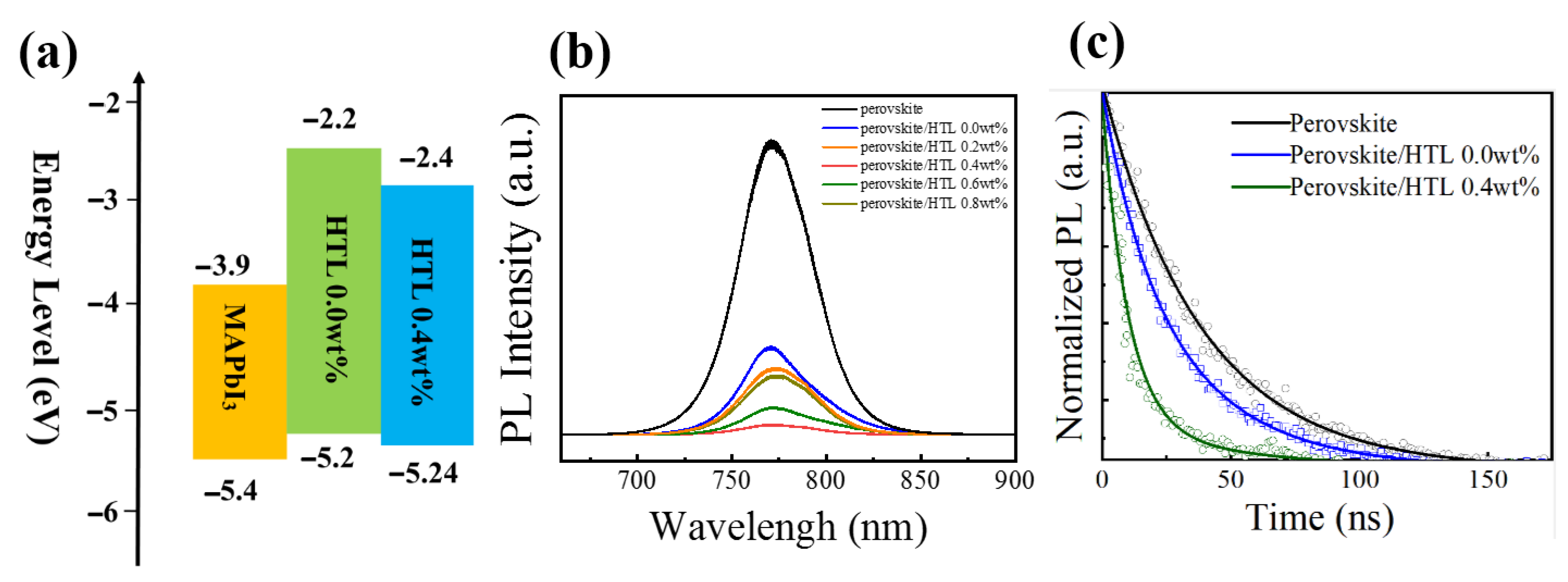
To better understand the effect of the dopants on the energy level of HTLs, ultraviolet photoemission spectra (UPS) are performed. As shown in Figure 6a, the energy level of HTLs can be obtained by the following equations: [34,35]. ECB = EVB + Eg; EVB = EF − Eonset (onset energy); EF = Ecutoff (cutoff energy) −21.22 eV. The ECB, EVB, EF, and Eg represent the conduction band maximum, valence band maximum, the Fermi level, and energy bandgap, respectively. The exact energy level values for the different HTLs are summarized in Table 1. After 0.4 wt% CsI doping, the Fermi level value of Spiro-OMeTAD film increases from −4.92 eV to –4.88 eV, indicating the formation of extensive p-type oxidized Spiro-OMeTAD+ cations. Figure 7a shows the energy levels of perovskite, HTL 0.0 wt%, and HTL 0.4 wt% layers. After 0.4 wt% CsI is added, the EVB of Spiro-OMeTAD film decreased from −5.21 eV to −5.24 eV. It is worth noting that the addition of CsI shifts downward the EVB of the HTL, which is closer to the EVB of perovskite, thus enabling more effective hole extraction and transportation between perovskite and HTL.
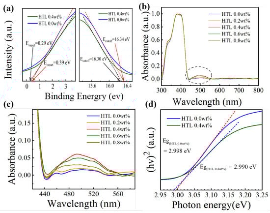
Figure 6.
(a) UPS diagrams of HTL 0.0 wt% and HTL 0.4 wt% films: Eonset area (left), Ecutoff area (right). (b) Ultraviolet-visible absorption spectra of Spiro-OMeTAD doped with different CsI content. (c) magnified image of the oxidized Spiro-OMeTAD peak at 440–560 nm. (d) Tauc plots of the HTL 0.0 wt%t and HTL 0.4 wt%.

Table 1.
The calculated values of energy level of the HTLs doped with and without CsI.
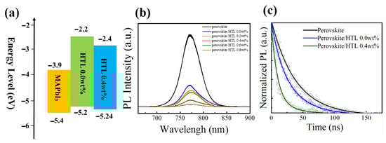
Figure 7.
(a) Energy levels of the perovskite, HTL 0.0 wt% and HTL 0.4 wt% layers. (b) PL spectra of perovskite and perovskite/Spiro-OMeTAD with different concentrations of CsI. (c) Time-resolved photoluminescence (TRPL) of perovskite and perovskite/HTL 0.0 wt% and perovskite/HTL 0.4 wt% layers.
To understand the properties of Spiro-OMeTAD: CsI (0.0, 0.2, 0.4, 0.6, 0.8 wt%) films with different doped concentrations, the UV-visible absorption spectra of Spiro-OMeTAD: CsI is characterized in the wavelength range from 300 to 800 nm. As shown in Figure 6b, all spectra are intensity normalized to the prominent peak at 390 nm [36,37]. The peaks of all samples near 390 nm can be attributed to Spiro-OMeTAD absorption, corresponding to the p-p* electron transition of Spiro-OMeTAD [38]. The broad peak around 500 nm shown in Figure 6c is the indicator for the generation of oxidized Spiro-OMeTAD (Spiro-OMeTAD+) [39,40,41]. However, HTL 0.4 wt% has the highest absorption peak near 500 nm, indicating that this concentration can effectively oxidize Spiro-OMeTAD. The formation of oxidized state Spiro-OMeTAD is beneficial to improving the hole’s mobility [42]. The evenly distributed Li-TFSI promoted the oxidation of Spiro-OMeTAD, which improves the hole mobility and the device’s overall performance. The doping of inorganic ions can improve the conductivity and carrier mobility of organic semiconductor materials and improve device stability [43,44]. As shown in Figure 6d, the energy bandgap (Eg) of HTL 0.4 wt% and HTL 0.0 wt% are 2.990 eV and 2.998 eV, respectively, and the difference is within the margin of error, indicating that adding CsI brings no noticeable impact on the bandgaps.
Photoluminescence (PL) spectroscopies further investigate the charge carrier dynamics of ITO/perovskite/HTL devices. Electron-hole pair be generated when the perovskite excites by laser, the radiation combination of the electron-hole pair will produce fluorescence. The hole extraction ability of HTL can be determined by comparing the fluorescence quenching effect of perovskite/Spiro-OMeTAD films [45]. As shown in Figure 7b the fluorescence intensity of Spiro-OMeTAD film doped with CsI is lower than that of the undoped film (HTL 0.0 wt%). HTL 0.4 wt% has the lowest fluorescence intensity. The results indicate that CsI doped could effectively improve the hole extractive ability of Spiro-OMeTAD films.
The process of hole extraction is analyzed by time-resolved photoluminescence (TRPL) decay spectra (Figure 7c). A bi-exponential equation can fit the TRPL decay curves:
Charge carrier average lifetime (τav) are 38.12 ns, 16.40 ns, and 10.06 ns for the pristine perovskite, perovskite/HTL 0.0 wt%, and perovskite/HTL 0.0 wt%, respectively (Table S2). The above indicates that CsI doped HTL has a faster and more efficient hole extraction ability, thus improving the photoelectric performance of the device [23,46]. Hole extraction rate where τ0 and τ represent the PL lifetime of the pristine perovskite and perovskite/HTL films, respectively. The hole extraction rate of perovskite/HTL 0.4 wt% is 7.32 × 10⁷ s−1, which is higher than perovskite/HTL 0.0 wt% (3.4 × 10⁷ s−1). HTL 0.4 wt% has a higher charge-carrier extraction ability, indicating that CsI doped can improve the perovskite/HTL interface and reduce defects of HTL.
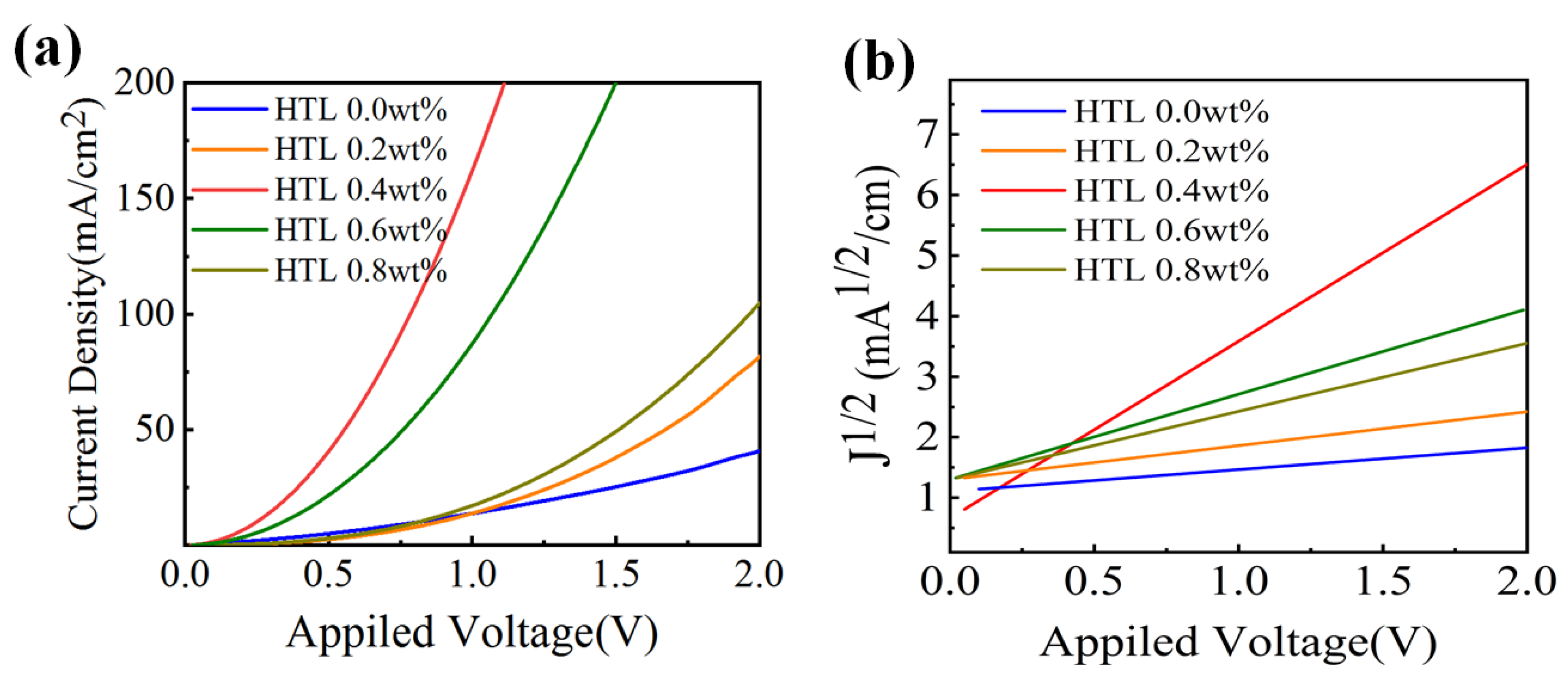
In order to study the carrier behaviour of the CsI-doped Spiro-OMeTAD film, a pure hole device is fabricated. Figure 8a shows the pure hole device’s current density–voltage curves in the 0–2 V voltage range, and Figure 8b shows the corresponding J1/2-V curves. Under the same voltage, the current density of CsI doped devices is much higher than the undoped ones. The device doped with 0.4 wt% CsI shows the highest current density in the whole bias range. The above indicates that the introduction of CsI improves the interface contact between the perovskites/HTL/electrode and makes the charge transfer faster. The mobilities of different HTLs are measured by space-charge-limited current (SCLC).
where εr = 3 is the dielectric constant of the Spiro-OMeTAD film, ε0 is the permittivity of free space, L = 200 nm is the thickness of Spiro-OMeTAD film, μ is the hole mobility, and V is the partial voltage. Based on the slope and intercept of the J1/2-V curves, we calculated the mobility of HTL by Equation (2). The hole mobility of HTL 0.4 wt% is 4.29 × 10⁻³ cm2 V−1 s−1, which is higher than the 2.12×10⁻⁴ cm2 V−1 s−1 of HTL 0.0 wt%. The above results verify that the introduction of CsI affects carrier behaviour. The above results verify that CsI improves the hole mobility of Spiro-OMeTAD, which helped the device achieve efficient hole transport and extraction, reducing dark currents and improving detection.
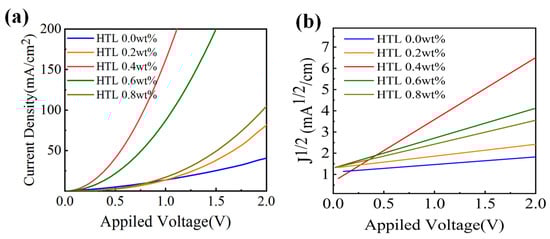
Figure 8.
(a) J-V and (b) J1/2-V curves in hole only devices with the structure of ITO/PEDOT: PSS (40 nm)/Spiro-OMeTAD (200 nm)/MoO3 (10 nm)/Cu.
3.2. Performance of the PSCs
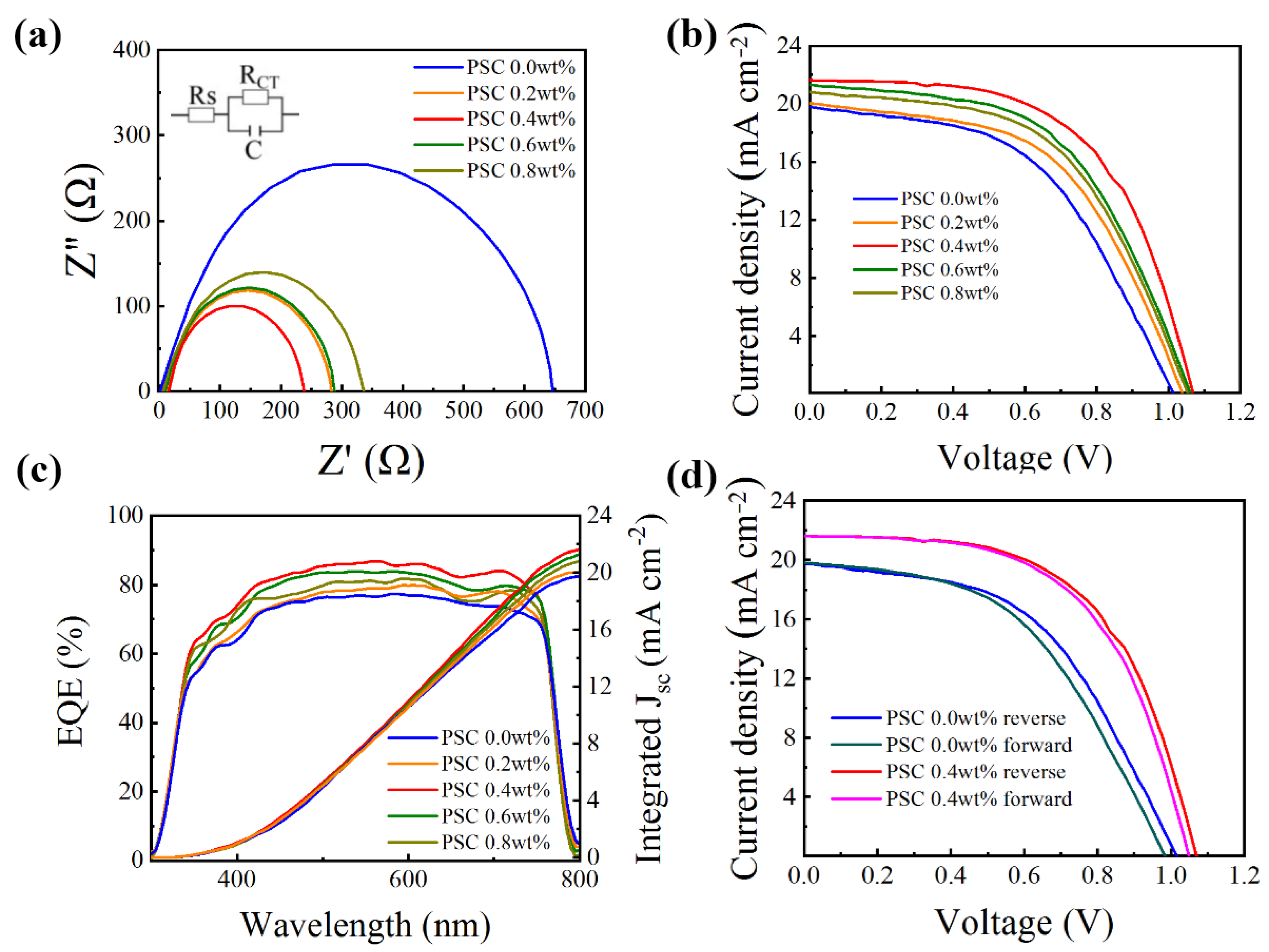
In order to further study the effect of doped CsI on the MAPbI3/HTL/MoO3/Cu interface, electrochemical impedance spectroscopy (EIS) measurement is performed on PSCs. Figure 9a shows the EIS spectrum of PSCs, and the inset is the equivalent circuit used to fit the data. The semicircle at high frequency is considered the charge transfer resistance (Rt) of the interface between MAPbI3/HTL and HTL/MoO3/Cu [47]. It is evident that the Spiro-OMeTAD doped with CsI has a lower Rt than the Spiro-OMeTAD without CsI doping. Among them, the semicircle of PSC 0.4 wt% is the smallest, indicating that the Spiro-OMeTAD film is the smoothest at this doping concentration, which is beneficial to the rapid transmission and extraction of holes. This result is consistent with Figure 9b, and the decreased Rt lad to higher FF and VOC of PSCs.
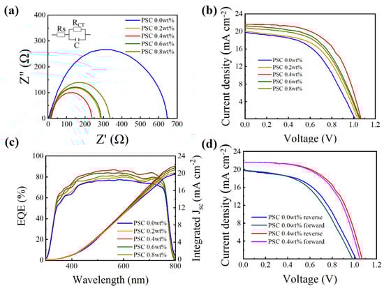
Figure 9.
(a) Nyquist plots of the PSCs based on different Spiro-OMeTADs. (b) J-V characteristics of devices with HTLs doping with different concentrations of CsI measured under AM 1.5 G solar irradiance (100 mW cm−2). (c) The EQE curve of the PSCs is based on Spiro-OMeTAD with different CsI doping concentrations. (d) J-V characteristics of PSC 0.0 wt% and PSC 0.4 wt%, measured at both forward and reverse scanning directions.
The optimal current-voltage (J-V) characteristic curve of devices based on the Spiro-OMeTAD with various doping concentrations of CsI (0.0, 0.2, 0.4, 0.6, 0.8 wt%) under simulated AM 1.5 G solar irradiation (100 mW cm−2) are displayed in Figure 9b, and their relevant photovoltaic parameters are summarized in Table 2. Compared with the PSC 0.0 wt%, the PSC optimized with different proportions of CsI result in significant increments in open-circuit voltage (VOC), short-circuit current (JSC) and fill factor (FF). In particular, PSC 0.4 wt% achieved the highest PCE value of 13.31% with a VOC of 1.07 V, a JSC of 23.09 mA cm−2, and a fill factor of 0.58. In contrast, the non-CsI-optimized device (PSC 0.0 wt%) has a PCE value of 10.02%, a VOC of 1.00 V, a JSC of 19.76 mA cm−2, and a fill factor of 0.50. The increased JSC and FF of PSCs are attributed to the optimized HTL [48], efficiently transporting holes from the perovskite layer. After the addition of CsI, the enhancement of the hole transportability of HTL reduces the accumulation of interface charges, thereby increasing the VOC of the device.
Table 2.
Photovoltaic data of PSCs based on Spiro-OMeTAD doped different CsI concentrations.
In order to explore the reproducibility of device efficiency, we made 20 PSC devices without CsI and with CsI optimization and measured them. Figure S6 shows the statistics of all devices. The PCE distribution of CsI optimized devices is concentrated in a small range of 12.68~13.31%, higher than the PCE distribution of devices without CsI (8.71~10.02%), indicating that our PSCs production process has good repeatability. As shown in Figure S6, the PCE first increases with CsI doping concentration. This is because doping CsI helps improve the charge transport performance of HTL. Moreover, a further increase in the CsI concentration will decrease short-circuit current density, open-circuit voltage, and influence factor. The accumulation of interface charge is one of the main reasons of the decrease in the light pressure of the device. We believe that the decrease in VOC can be attributed to the increase in SnO2/perovskite/HTL interface charge recombination. The previous analysis shows that an appropriate amount of CsI doping concentration can improve the hole mobility of Spiro-OMeTAD (Figure 8 and Table 3), which is conducive to the charge transport of HTL. When the doped CsI concentration is 0.4 wt% (mass ratio, CsI/TBP), PSCs have the best PCE. As the CsI concentration further increases, the PCE of the device decreases. This is because excessive CsI that does not form a complex with TBP may act as a recombination centereat the interface between perovskite and HTL, thereby increasing the hole concentration in HTM and reducing the driving force for hole extraction, resulting in a device Performance deteriorating. Therefore, the doping amount of CsI concentration of about 0.4 wt% (mass ratio, CsI/TBP) may be the balance point of hole extraction, hole transport, and interface recombination.
Table 3.
The mobility of HTL consisting of Spiro-OMeTAD and different amounts of CsI (0.0, 0.2, 0.4, 0.6, and 0.8 wt%).
Figure 9c shows the EQE curve of solar cells with or without CsI dopants. Obviously, the CsI-doped Spiro-OMeTAD device exhibits a higher EQE in the 300–800 nm region than the undoped Spiro-OMeTAD. As mentioned above, this may be due to the high hole mobility and conductivity of CsI-doped HTL. The integral JSC value obtained from the EQE curve is basically the same as the value obtained from the J-V characteristics curve, indicating the validity of our measurement.
As we all know, in the PSCs measurement process, the J-V characteristic curve will change due to the different scanning directions and scanning rate [49]. As shown in Figure 9d, we studied the hysteresis in PSCs through reverse and forward scanning. The hysteresis index (HI) is used to estimate the degree of hysteresis: HI = (PCEreverse − PCEforward)/PCE reverse. The detailed photovoltaic parameters are shown in Table 4. From Table 4, we can know that the HI of the PSC 0.0 wt% is 0.082, but it reduced to 0.031 after optimization by CsI. This shows that CsI optimized devices have lower hysteresis. The reason for the decrease in hysteresis may be that the conductivity of the HTL is optimized, the carrier extraction capability of the HTL is enhanced, and the traps at the perovskite/HTL interface are passivated so that electron transport and hole transport are balanced [50].
Table 4.
Photovoltaic data of the PSC 0.0 wt% and PSC 0.4 wt% measured in forward and reversed scans.
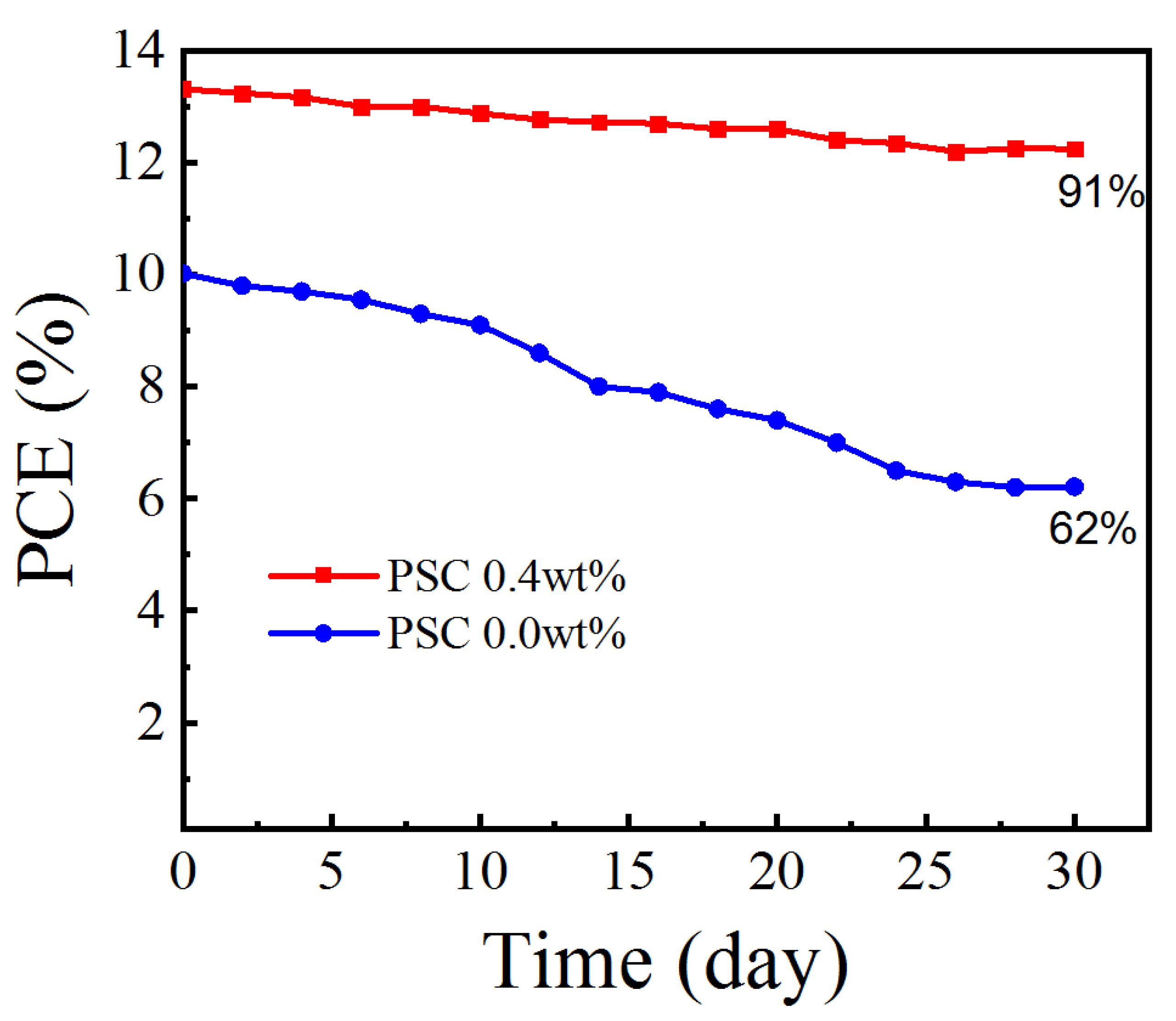
As shown in Figure 10, the stability of Spiro-OMeTAD-doped or non-doped CsI PSCs is tested for about 30 days (relative humidity: 25%RH, temperature: 25 °C). During the 30d storage period, the PCE 0.0 wt% device value is significantly reduced to 62% of the original value, while the CsI optimized PCE 0.4 wt% device maintained 91% of its initial PCE value, showing excellent long-term stability.
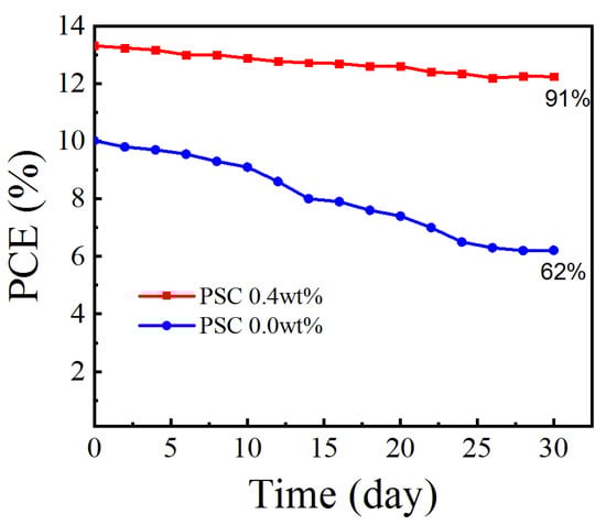
Figure 10.
Stability test for the efficiencies of the unpackaged devices based on doped or undoped Spiro-OMeTAD HTLs.
The degradation of device performance is a combination of many factors. The deterioration of the perovskite/transport layer interface and the decomposition of perovskite crystals may lead to the degradation of solar cell performance. Fu et al. found that at higher operating temperatures, the degradation mainly starts from the inside of the perovskite absorber rather than the perovskite/charge-selective layer interface or the cell edge [51]. Khadka et al. found that voids at the HTL (ETL)/HaP interface and I2 gas released from PbI2 crystallites are the main reasons for the degradation of perovskite solar cells [52]. In this work, we found that the main reason for the performance degradation of solar cells is that the surface of the hole transport layer of Spiro-OMeTAD not optimized by CsI is rough and had voids, which allows the intrusion of moisture from the air. Moisture penetrating the Spiro-OMeTAD hole transport layer will destroy the perovskite layer and cause the perovskite to decompose. The hydrolytic reaction of perovskite conforms to the following stoichiometric equation: [53].
According to the chemical equation, the water reacts with the perovskite layer, breaking the perovskite into PbI2. After optimization, the stability of the PSC 0.4 wt% device is enhanced. This is because HTL 0.4 wt% has a dense and uniform surface film, which can effectively prevented moisture intrusion. The dense hole transport layer protects the perovskite layer and increase the stability of perovskite solar cells.
4. Conclusions
In summary, we use a mixture of Spiro-OMeTAD, Li-TFSI, TBP and CsI as HTL, showing a cheap and straightforward strategy to improve the photovoltaic performance of PSCs. CsI and TBP form a complex, which effectively prevents the rapid evaporation of TBP, reduce the defects between the perovskite/HTL, and makes the surface of Spiro-OMeTAD uniform and smooth. UV-Vis absorption spectra, PL and TRPL results show that doping CsI can effectively oxidize Spiro-OMeTAD to Spiro-OMeTAD+, which improves the hole extraction ability of HTL. In addition, SCLC, UPS, and EIS analysis confirmed that HTM doped with CsI improves the conductivity of HTL, reduces charge recombination loss, and achieves an appropriate energy level. In particular, the addition of CsI increases the short-circuit current density and open-circuit voltage of the PSC, mainly due to the increase in the extraction rate of holes and the reduction of carrier recombination. Therefore, under the same conditions, the maximum PCE value of the PSC 0.4 wt% optimized by CsI is 13.31%, while the PCE value of the unoptimized PSC 0.0 wt% device is only 10.01%. At the same time, the 0.4 wt% CsI-doped device maintained an initial efficiency of 91% within 30 days (humidity: 25%, temperature: 25 °C, dark conditions), while the original device only maintained a efficiency of 62%. This work provides a simple and low-cost method for improving PSCs’ photovoltaic performance and stability.
Supplementary Materials
The following supporting information can be downloaded at: https://www.mdpi.com/article/10.3390/cryst12020290/s1, Figure S1: (a–e) Top-view SEM images of fresh Spiro-OMeTAD film (HTL 0.0wt%, HTL 0.2wt%, HTL 0.4wt%, HTL 0.6wt% and HTL 0.8wt%) after spin coating. (f–k) Top view SEM image of the corresponding Spiro-OMeTAD film after being oxidized in air for 8 hours. (l–p) Top view 3D AFM image of the corresponding Spiro-OMeTAD film after oxidation in air for 8 hours. Figure S2: (a) Elementary characterization of HTL 0.0wt%; (b,c) EDS mapping of S and F elements in HTL 0.0wt%. Figure S3: (a) Elementary characterization of HTL 0.4wt%; (b–e) EDS mapping of Cs, S, I and F elements in HTL 0.4wt%. Figure S4: Top-view SEM image of the perovskite film. Figure S5: Water contact angles of ITO/SnO2/perovskite/HTL 0.0wt% (a-c) and ITO/SnO2/perovskite/HTL 0.4wt% (d). Figure S6: At five concentrations of 0.0, 0.2, 0.4, 0.6 and 0.8 wt% (mass ratio, CsI/TBP). The statistical distribution of Voc (a), Jsc (b), FF (c) and PCE (d) photovoltaic parameters of 20 PSCs samples under the same test conditions. Table S1: AFM data of Spiro-OMeTAD doped with different mass ratio of CsI. Table S2: TRPL data of ITO/Perovskite, ITO/Perovskite/HTL 0.0wt% and ITO/ Perovskite/HTL 0.4wt%.
Author Contributions
Y.W. and W.S. conceived the idea; G.L. designed the experiments; G.L. and L.H. carried out the device fabrication; G.L. and L.H. carried out electrical characterizations and the optical characterizations; Administration: R.Z. All authors have read and agreed to the published version of the manuscript.
Funding
This research received no external funding.
Acknowledgments
This work is supported financially by the fund for Bagui Talent of Guangxi Province (No. T3120097921, No. T31200992001), Talent Model Base (AD19110157), Guangxi Science and Technology Program (AD19245132), Guangxi University Foundation (A3120051010). Guangxi Science and Technology Base and Talent Special project (No. AD20238093, No. AE31200086), and Disinfection Robot Based on High Power AlGaN-based UVLEDs (No.BB31200014).
Conflicts of Interest
The authors declare no conflict of interest.
References
- Huang, L.; Wang, Y.; Zhu, X.; Zhao, X.; Li, G.; Li, L.; Sun, W. Mg-Doped Nickel Oxide as Efficient Hole-Transport Layer for Perovskite Photodetectors. J. Phys. Chem. C 2021, 125, 16066–16074. [Google Scholar] [CrossRef]
- Zhao, X.; Huang, L.; Wang, Y.; Zhu, X.; Li, L.; Li, G.; Sun, W. Interface engineering for gain perovskite photodetectors with extremely high external quantum efficiency. RSC Adv. 2020, 10, 32976–32983. [Google Scholar] [CrossRef]
- Miyata, A.; Mitioglu, A.; Plochocka, P.; Portugall, O.; Wang, J.T.-W.; Stranks, S.D.; Snaith, H.J.; Nicholas, R.J. Direct measurement of the exciton binding energy and effective masses for charge carriers in organic–inorganic tri-halide perovskites. Nat. Phys. 2015, 11, 582–587. [Google Scholar] [CrossRef] [Green Version]
- Dong, Q.; Fang, Y.; Shao, Y.; Mulligan, P.; Qiu, J.; Cao, L.; Huang, J. Electron-hole diffusion lengths > 175 μm in solution-grown CH3NH3PbI3 single crystals. Science 2015, 347, 967–970. [Google Scholar] [CrossRef] [Green Version]
- Zhao, X.; Wang, Y.; Li, L.; Huang, L.; Li, G.; Sun, W.H. Methylammonium Chloride reduces the bandgap width and trap densities for efficient perovskite photodetectors. J. Mater. Sci. 2021, 56, 9242–9253. [Google Scholar] [CrossRef]
- Zhu, X.; Zhao, X.; Li, L.; Peng, Y.; Wei, W.; Zhang, X.; Su, M.; Wang, Y.; Chen, Z.; Sun, W. Perovskite Self-Passivation with PCBM for Small Open-Circuit Voltage Loss. Energy Power Eng. 2020, 12, 257–272. [Google Scholar] [CrossRef]
- Snaith, H.J. Perovskites: The Emergence of a New Era for Low-Cost, High-Efficiency Solar Cells. J. Phys. Chem. Lett. 2013, 4, 3623–3630. [Google Scholar] [CrossRef]
- Song, Z.; McElvany, C.L.; Phillips, A.B.; Celik, I.; Krantz, P.W.; Watthage, S.C.; Liyanage, G.K.; Apul, D.; Heben, M.J. A technoeconomic analysis of perovskite solar module manufacturing with low-cost materials and techniques. Energy Environ. Sci. 2017, 10, 1297–1305. [Google Scholar] [CrossRef]
- McMeekin, D.P.; Mahesh, S.; Noel, N.K.; Klug, M.T.; Lim, J.; Warby, J.H.; Ball, J.M.; Herz, L.M.; Johnston, M.B.; Snaith, H.J. Solution-Processed All-Perovskite Multi-junction Solar Cells. Joule 2019, 3, 387–401. [Google Scholar]
- Nie, W.; Tsai, H.; Asadpour, R.; Blancon, J.-C.; Neukirch Amanda, J.; Gupta, G.; Crochet Jared, J.; Chhowalla, M.; Tretiak, S.; Alam Muhammad, A.; et al. High-efficiency solution-processed perovskite solar cells with millimeter-scale grains. Science 2015, 347, 522–525. [Google Scholar] [CrossRef] [PubMed] [Green Version]
- Kojima, A.; Teshima, K.; Shirai, Y.; Miyasaka, T. Organometal Halide Perovskites as Visible-Light Sensitizers for Photovoltaic Cells. J. Am. Chem. Soc. 2009, 131, 6050–6051. [Google Scholar] [CrossRef] [PubMed]
- Ryu, S.; Noh, J.; Jeon, N.; Kim, Y.; Yang, W.; Seo, J.; Im, S.H. Voltage output of efficient perovskite solar cells with high open-circuit voltage and fill factor. Energy Environ. Sci. 2014, 7, 2614–2618. [Google Scholar] [CrossRef]
- Guo, R.; Huang, F.; Zheng, K.; Pullerits, T.; Tian, J. CuInSe2 Quantum Dots Hybrid Hole Transfer Layer for Halide Perovskite Photodetectors. ACS Appl. Mater. Interfaces 2018, 10, 35656–35663. [Google Scholar] [CrossRef]
- Zhou, H.; Yang, L.; Gui, P.; Grice, C.R.; Song, Z.; Wang, H.; Fang, G. Ga-doped ZnO nanorod scaffold for high-performance, hole-transport-layer-free, self-powered CH3NH3PbI3 perovskite photodetectors. Sol. Energy Mater. Sol. Cells 2019, 193, 246–252. [Google Scholar] [CrossRef]
- Ghosh, J.; Natu, G.; Giri, P.K. Plasmonic hole-transport-layer enabled self-powered hybrid perovskite photodetector using a modified perovskite deposition method in ambient air. Org. Electron. 2019, 71, 175–184. [Google Scholar] [CrossRef]
- Yu, W.; Sun, X.; Xiao, M.; Hou, T.; Liu, X.; Zheng, B.; Yu, H.; Zhang, M.; Huang, Y.; Hao, X. Recent advances on interface engineering of perovskite solar cells. Nano Res. 2022, 15, 85–103. [Google Scholar] [CrossRef]
- Lin, C.H.; Hu, L.; Guan, X.; Kim, J.; Huang, C.Y.; Huang, J.K.; Singh, S.; Wu, T.J.A.M. Electrode Engineering in Halide Perovskite Electronics: Plenty of Room at the Interfaces. Adv. Mater. 2022, 2108616. [Google Scholar] [CrossRef]
- Leijtens, T.; Lim, J.; Teuscher, J.; Park, T.; Snaith, H.J. Charge Density Dependent Mobility of Organic Hole-Transporters and Mesoporous TiO2 Determined by Transient Mobility Spectroscopy: Implications to Dye-Sensitized and Organic Solar Cells. Adv. Mater. 2013, 25, 3227–3233. [Google Scholar] [CrossRef]
- Burschka, J.; Dualeh, A.; Kessler, F.; Baranoff, E.; Cevey-Ha, N.-L.; Yi, C.; Nazeeruddin, M.K.; Grätzel, M. Tris(2-(1H-pyrazol-1-yl)pyridine)cobalt(III) as p-Type Dopant for Organic Semiconductors and Its Application in Highly Efficient Solid-State Dye-Sensitized Solar Cells. J. Am. Chem. Soc. 2011, 133, 18042–18045. [Google Scholar] [CrossRef] [PubMed]
- Schloemer, T.H.; Christians, J.A.; Luther, J.M.; Sellinger, A. Doping strategies for small molecule organic hole-transport materials: Impacts on perovskite solar cell performance and stability. Chem. Sci. 2019, 10, 1904–1935. [Google Scholar] [CrossRef] [Green Version]
- Ono, L.K.; Schulz, P.; Endres, J.J.; Nikiforov, G.O.; Kato, Y.; Kahn, A.; Qi, Y. Air-Exposure-Induced Gas-Molecule Incorporation into Spiro-MeOTAD Films. J. Phys. Chem. Lett. 2014, 5, 1374–1379. [Google Scholar] [CrossRef] [PubMed]
- Liu, Y.; Hu, Y.; Zhang, X.; Zeng, P.; Li, F.; Wang, B.; Yang, Q.; Liu, M. Inhibited aggregation of lithium salt in spiro-OMeTAD toward highly efficient perovskite solar cells. Nano Energy 2020, 70, 104483. [Google Scholar] [CrossRef]
- Yuan, P.; Wu, J.; Sun, W.; Zhu, Q.; Zhang, M.; Zou, J.; Wang, X.; Liu, X.; Yang, Y.; Lan, Z. High-Performance Perovskite Solar Cells Using Iodine as Effective Dopant for Spiro-OMeTAD. Energy Technol. 2020, 8, 1901171. [Google Scholar] [CrossRef]
- Wang, S.; Sina, M.; Parikh, P.; Uekert, T.; Shahbazian, B.; Devaraj, A.; Meng, Y.S. Role of 4-tert-Butylpyridine as a Hole Transport Layer Morphological Controller in Perovskite Solar Cells. Nano Lett. 2016, 16, 5594–5600. [Google Scholar] [CrossRef]
- Noh, J.H.; Jeon, N.J.; Choi, Y.C.; Nazeeruddin, M.K.; Grätzel, M.; Seok, S.I. Nanostructured TiO2/CH3NH3PbI3 heterojunction solar cells employing spiro-OMeTAD/Co-complex as hole-transporting material. J. Mater. Chem. A 2013, 1, 11842–11847. [Google Scholar] [CrossRef]
- Xu, M.; Rong, Y.; Ku, Z.; Mei, A.; Li, X.; Han, H. Improvement in Solid-State Dye Sensitized Solar Cells by p-Type Doping with Lewis Acid SnCl4. J. Phys. Chem. C 2013, 117, 22492–22496. [Google Scholar] [CrossRef]
- Chen, D.-Y.; Tseng, W.-H.; Liang, S.-P.; Wu, C.-I.; Hsu, C.-W.; Chi, Y.; Hung, W.-Y.; Chou, P.-T. Application of F4TCNQ doped spiro-MeOTAD in high performance solid state dye sensitized solar cells. Phys. Chem. Chem. Phys. 2012, 14, 11689–11694. [Google Scholar] [CrossRef] [PubMed]
- Zhang, J.; Zhang, T.; Jiang, L.; Bach, U.; Cheng, Y.-B. 4-tert-Butylpyridine Free Hole Transport Materials for Efficient Perovskite Solar Cells: A New Strategy to Enhance the Environmental and Thermal Stability. ACS Energy Lett. 2018, 3, 1677–1682. [Google Scholar] [CrossRef]
- Niu, X.; Li, N.; Zhu, C.; Liu, L.; Zhao, Y.; Ge, Y.; Chen, Y.; Xu, Z.; Lu, Y.; Sui, M.; et al. Temporal and spatial pinhole constraints in small-molecule hole transport layers for stable and efficient perovskite photovoltaics. J. Mater. Chem. A 2019, 7, 7338–7346. [Google Scholar] [CrossRef]
- Yang, Z.; Dou, J.; Wang, M.; Li, J.; Huang, J.; Shao, J. Flexible all-inorganic photoconductor detectors based on perovskite/hole-conducting layer heterostructures. J. Mater. Chem. C 2018, 6, 6739–6746. [Google Scholar] [CrossRef]
- Juarez-Perez, E.J.; Leyden, M.R.; Wang, S.; Ono, L.K.; Hawash, Z.; Qi, Y. Role of the Dopants on the Morphological and Transport Properties of Spiro-MeOTAD Hole Transport Layer. Chem. Mater. 2016, 28, 5702–5709. [Google Scholar] [CrossRef]
- Boyd, C.C.; Cheacharoen, R.; Leijtens, T.; McGehee, M.D. Understanding Degradation Mechanisms and Improving Stability of Perovskite Photovoltaics. Chem. Rev. 2019, 119, 3418–3451. [Google Scholar] [CrossRef]
- Cappel, U.B.; Daeneke, T.; Bach, U. Oxygen-Induced Doping of Spiro-MeOTAD in Solid-State Dye-Sensitized Solar Cells and Its Impact on Device Performance. Nano Lett. 2012, 12, 4925–4931. [Google Scholar] [CrossRef]
- Dou, Y.; Wang, D.; Li, G.; Liao, Y.; Sun, W.; Wu, J.; Lan, Z. Toward Highly Reproducible, Efficient, and Stable Perovskite Solar Cells via Interface Engineering with CoO Nanoplates. ACS Appl. Mater. Interfaces 2019, 11, 32159–32168. [Google Scholar] [CrossRef] [PubMed]
- Peng, J.; Chen, Y.; Zheng, K.; Pullerits, T.; Liang, Z. Insights into charge carrier dynamics in organo-metal halide perovskites: From neat films to solar cells. Chem. Soc. Rev. 2017, 46, 5714–5729. [Google Scholar] [CrossRef] [PubMed] [Green Version]
- Ding, I.K.; Tétreault, N.; Brillet, J.; Hardin, B.E.; Smith, E.H.; Rosenthal, S.J.; Sauvage, F.; Grätzel, M.; McGehee, M.D. Pore-Filling of Spiro-OMeTAD in Solid-State Dye Sensitized Solar Cells: Quantification, Mechanism, and Consequences for Device Performance. Adv. Funct. Mater. 2009, 19, 2431–2436. [Google Scholar] [CrossRef]
- Schölin, R.; Karlsson, M.H.; Eriksson, S.K.; Siegbahn, H.; Johansson, E.M.J.; Rensmo, H. Energy Level Shifts in Spiro-OMeTAD Molecular Thin Films When Adding Li-TFSI. J. Phys. Chem. C 2012, 116, 26300–26305. [Google Scholar] [CrossRef]
- Li, Z.; Wu, J.; Liu, X.; Zhu, Q.; Yang, Y.; Dou, Y.; Du, Y.; Zhang, X.; Chen, Q.; Sun, W.; et al. Highly efficient and stable perovskite solar cells using thionyl chloride as a p-type dopant for spiro-OMeTAD. J. Alloys Compd. 2020, 847, 156500. [Google Scholar] [CrossRef]
- Ashassi-Sorkhabi, H.; Salehi-Abar, P. How the change of OMe substituent position affects the performance of spiro-OMeTAD in neutral and oxidized forms: Theoretical approaches. RSC Adv. 2018, 8, 18234–18242. [Google Scholar] [CrossRef] [Green Version]
- Cappel, U.B.; Gibson, E.A.; Hagfeldt, A.; Boschloo, G. Dye Regeneration by Spiro-MeOTAD in Solid State Dye-Sensitized Solar Cells Studied by Photoinduced Absorption Spectroscopy and Spectroelectrochemistry. J. Phys. Chem. C 2009, 113, 6275–6281. [Google Scholar] [CrossRef]
- Fantacci, S.; De Angelis, F.; Nazeeruddin, M.K.; Grätzel, M. Electronic and Optical Properties of the Spiro-MeOTAD Hole Conductor in Its Neutral and Oxidized Forms: A DFT/TDDFT Investigation. J. Phys. Chem. C 2011, 115, 23126–23133. [Google Scholar] [CrossRef] [Green Version]
- Scully, S.R.; Armstrong, P.B.; Edder, C.; Fréchet, J.M.J.; McGehee, M.D. Long-Range Resonant Energy Transfer for Enhanced Exciton Harvesting for Organic Solar Cells. Adv. Mater. 2007, 19, 2961–2966. [Google Scholar] [CrossRef]
- Kröger, M.; Hamwi, S.; Meyer, J.; Riedl, T.; Kowalsky, W.; Kahn, A. Role of the deep-lying electronic states of MoO3 in the enhancement of hole-injection in organic thin films. Appl. Phys. Lett. 2009, 95, 123301. [Google Scholar] [CrossRef]
- Small, C.E.; Tsang, S.-W.; Kido, J.; So, S.K.; So, F. Origin of Enhanced Hole Injection in Inverted Organic Devices with Electron Accepting Interlayer. Adv. Funct. Mater. 2012, 22, 3261–3266. [Google Scholar] [CrossRef]
- Pockett, A.; Eperon, G.E.; Peltola, T.; Snaith, H.J.; Walker, A.; Peter, L.M.; Cameron, P.J. Characterization of Planar Lead Halide Perovskite Solar Cells by Impedance Spectroscopy, Open-Circuit Photovoltage Decay, and Intensity-Modulated Photovoltage/Photocurrent Spectroscopy. J. Phys. Chem. C 2015, 119, 3456–3465. [Google Scholar] [CrossRef] [Green Version]
- Dou, L.; Yang, Y.; You, J.; Hong, Z.; Chang, W.-H.; Li, G.; Yang, Y. Solution-processed hybrid perovskite photodetectors with high detectivity. Nat. Commun. 2014, 5, 5404. [Google Scholar] [CrossRef]
- Li, Z.; Tinkham, J.; Schulz, P.; Yang, M.; Kim, D.H.; Berry, J.; Sellinger, A.; Zhu, K. Acid Additives Enhancing the Conductivity of Spiro-OMeTAD Toward High-Efficiency and Hysteresis-Less Planar Perovskite Solar Cells. Adv. Energy Mater. 2017, 7, 1601451. [Google Scholar] [CrossRef]
- Liu, X.; Cheng, Y.; Liu, C.; Zhang, T.; Zhang, N.; Zhang, S.; Chen, J.; Xu, Q.; Ouyang, J.; Gong, H. 20.7% highly reproducible inverted planar perovskite solar cells with enhanced fill factor and eliminated hysteresis. Energy Environ. Sci. 2019, 12, 1622–1633. [Google Scholar] [CrossRef]
- Snaith, H.J.; Abate, A.; Ball, J.M.; Eperon, G.E.; Leijtens, T.; Noel, N.K.; Stranks, S.D.; Wang, J.T.-W.; Wojciechowski, K.; Zhang, W. Anomalous Hysteresis in Perovskite Solar Cells. J. Phys. Chem. Lett. 2014, 5, 1511–1515. [Google Scholar] [CrossRef] [PubMed]
- Bai, D.; Zhang, J.; Jin, Z.; Bian, H.; Wang, K.; Wang, H.; Liang, L.; Wang, Q.; Liu, S.F. Interstitial Mn2+-Driven High-Aspect-Ratio Grain Growth for Low-Trap-Density Microcrystalline Films for Record Efficiency CsPbI2Br Solar Cells. ACS Energy Lett. 2018, 3, 970–978. [Google Scholar] [CrossRef]
- Fu, F.; Pisoni, S.; Jeangros, Q.; Sastre-Pellicer, J.; Kawecki, M.; Paracchino, A.; Moser, T.; Werner, J.; Andres, C.; Duchêne, L.; et al. I2 vapor-induced degradation of formamidinium lead iodide based perovskite solar cells under heat–light soaking conditions. Energy Environ. Sci. 2019, 12, 3074–3088. [Google Scholar] [CrossRef] [Green Version]
- Khadka, D.B.; Shirai, Y.; Yanagida, M.; Miyano, K. Insights into Accelerated Degradation of Perovskite Solar Cells under Continuous Illumination Driven by Thermal Stress and Interfacial Junction. ACS Appl. Energy Mater. 2021, 4, 11121–11132. [Google Scholar] [CrossRef]
- Leguy, A.M.A.; Hu, Y.; Campoy-Quiles, M.; Alonso, M.I.; Weber, O.J.; Azarhoosh, P.; van Schilfgaarde, M.; Weller, M.T.; Bein, T.; Nelson, J.; et al. Reversible Hydration of CH3NH3PbI3 in Films, Single Crystals, and Solar Cells. Chem. Mater. 2015, 27, 3397–3407. [Google Scholar] [CrossRef]

Publisher’s Note: MDPI stays neutral with regard to jurisdictional claims in published maps and institutional affiliations. |
© 2022 by the authors. Licensee MDPI, Basel, Switzerland. This article is an open access article distributed under the terms and conditions of the Creative Commons Attribution (CC BY) license (https://creativecommons.org/licenses/by/4.0/).