Article

Optimization of Effective Doping Concentration of Emitter for Ideal c-Si Solar Cell Device with PC1D Simulation

by
Maruthamuthu Subramanian
1,*,
Balaji Nagarajan
2,
Aishwarya Ravichandran
3,
Varsha Subhash Betageri
3,
Gokul Sidarth Thirunavukkarasu
3,
Elmira Jamei
4,
Mehdi Seyedmahmoudian
3,*,
Alex Stojcevski
3,
Saad Mekhilef
3 and
Vasudeva Reddy Minnam Reddy
5
1
Department of Physics, PSG Institute of Technology and Applied Research, Coimbatore 641062, India
2
Department of Energy Science, Sungkyunkwan University, Suwon 16419, Korea
3
School of Science, Computing and Engineering Technologies, Swinburne University of Technology, Melbourne, VIC 3122, Australia
4
College of Engineering and Science, Victoria University, Melbourne, VIC 3011, Australia
5
School of Chemical Engineering, Yeungnam University, 280 Gyeongsan, Gyeongsan 38541, Korea
*
Authors to whom correspondence should be addressed.
Crystals 2022, 12(2), 244; https://doi.org/10.3390/cryst12020244
Submission received: 16 December 2021 / Revised: 29 January 2022 / Accepted: 7 February 2022 / Published: 11 February 2022
(This article belongs to the Special Issue Silicon and Graphene Based Materials and Related Devices)

Abstract

:
Increasing silicon solar cell efficiency plays a vital role in improving the dominant market share of photo-voltaic systems in the renewable energy sector. The performance of the solar cells can be evaluated by making a profound analysis on various effective parameters, such as the sheet resistance, doping concentration, thickness of the solar cell, arbitrary dopant profile, etc., using software simulation tools, such as P C 1 D . In this paper, we present the observations obtained from the evaluation carried out on the impact of sheet resistance on the solar cell’s parameters using P C 1 D software. After which, the E D N A 2 simulation tool was used to analyse the emitter saturation current density for the chosen arbitrary dopant profile. Results indicated that the diffusion profile with low surface concentration and shallow junction depth can improve the blue response at the frontal side of the solar cell. The emitter saturation current density decreases from 66.52 to 36.82 fA/cm 2 for the subsequent increase in sheet resistance. The blue response also increased from 89.6 % to 97.5 % with rise in sheet resistance. In addition, the short circuit density and open circuit voltage was also observed to be improved by 0.6 mA/cm 2 and 3 mV for the sheet resistance value of 130 Ω /sq, which resulted in achieving the highest efficiency of 20.6 % .

1. Introduction

The energy demand and rate of electricity consumption has significantly increased with urbanization, technological advancements and population growth [1,2], which is primarily addressed by fossil-fuel-based conventional energy resources. The use of conventional energy resources leads to global warming and climate change creating adverse environmental impacts. Therefore, to reduce these impacts, renewable energy resources, such as solar, wind, tidal, biomass, hydro, and geothermal, are considered as an alternative energy generation sources. In addition to the environmental impacts, the renewable energy sources also provide economic and social impacts, thereby, making it a sustainable choice [3].
Solar photovoltaics are considered as a promising type of renewable energy resource due to the abundant availability and cost-effective nature leading to a production of about 200 to 350 W/m 2 in hot temperate climatic regions on average. Matthias et al. projected an installation capacity of about 800,000 km 2 of solar panels to meet the gross estimated demand of 16 TW highlighting the drawback of the very low ( 10 % ) conversion efficiency of the commercially available solar panels [4].
This alarming nature of the increasing demand and lower efficiency has motivated many researchers across the world to work on optimizing/improving the cell efficiency of the solar panels. Improvement of the efficiency of the solar panels is considered to be more significant than reducing the manufacturing costs when considering the proportional relationship with the rise in the solar cell efficiency and reduction of the cost. Therefore, many simulation and modelling software packages have been developed to simulate the impact of optimizing characteristics, such as the thickness of a solar cell, concentration level of doping elements, type of dopants used, and configuration of the contacts in the solar cell structure.
The crystalline silicon (c-Si) solar cell is the most common type of solar cell used world wide due to the simple structure and effective operating procedure. The c-Si solar cell mainly consists of a moderately doped p-type wafer in the middle with a highly doped n + layer on the top and p + layer on the rear side. In addition to this, an anti reflecting coating and serial connectors are present in the front side of the solar cell structure as illustrated in Figure 1.
From the literature, it is evident that the characteristics of emitter configuration of a c-Si solar cell has a significant influence on the efficiency and many researchers across the world are working towards improving this. State-of-the-art approaches are used to appropriately perform characterization and optimization of the emitter configurations that can lead to a significant efficiency gain; this efficiency gain substantially reduces the cost of the system.
An ideal emitter configuration aims to reduces the (i) recombination losses in the diffused region as well as at the surface of the cell and (ii) resistive losses [6] as the emitter doping profile plays a significant role in controlling the solar cell’s device characteristics. In a typical solar cell, the highly doped homogeneous emitter having a low sheet resistance ( R s h e e t ) of 40 50   Ω /sq, with a junction depth of 0.4–0.5 μ m is used. This heavily doped deeper emitter configurations reduces the contact resistance as highlighted by Stem et al.
However, this heavily doped emitter contributes in the reduction of the blue response as well as the surface passivation [7]. Optimization of I–V characteristics, such as the open circuit voltage ( V o c ), saturation current density ( J s c ) and fill factor ( F F ) play a significant role in increasing the conversion efficiency of the solar cell’s without altering its structure by developing an ideal emitter layer as highlighted by Franklin et al. [8].
By introducing a heavy diffusion in the emitter region, the solar cell efficiency can be improved. Therefore, Teinkemper et al. recommends the peak doping concentration should be higher to achieve higher efficiency of the solar cell [9]. However, the heavy doping concentration of the emitter improves the surface passivation, but this creates a drawback by increasing the contact resistivity. Doshi et al. highlighted that the increase in blue response with shallow junction depth, increases the shunting probability, which will influence the decline in the efficiency of the solar cell [10].
In conventional solar cell processing, emitter formation is a tedious and an expensive process that motivates researchers to conduct simulations before experimentally verifying the performance of the optimized emitter configurations [11]. P C 1 D is one of the widely used solar cell simulators [12], which will be used for evaluating of the emitter configurations, such as sheet resistance and emitter doping concentration in this paper. P C 1 D is an open-source, extremely informative, modelling tool that assists in the evaluation of all crucial factors constituting a solar cell.
P C 1 D allows the variation in parameters, such as bulk doping levels, variation in doping concentration of emitter etc. Moreover, we can visualize the performance of the I–V curve, V o c , J s c , external and internal quantum efficiencies of solar cell in a graphical format [13]. Kim et.al investigated the doping profile effect on the selective emitter solar cells by P C 1 D [14]. Park et al. studied the influence of the doping profile on the current density, generation rate, recombination rate. and defect density in c-Si solar cells using T C A D simulation [15].
In this present study, we explore the effects of higher sheet resistance of an emitter and analyse the impact on the performance of solar cells. Finally, a detailed analysis of the emitter saturation current density was performed with E D N A 2 simulation.

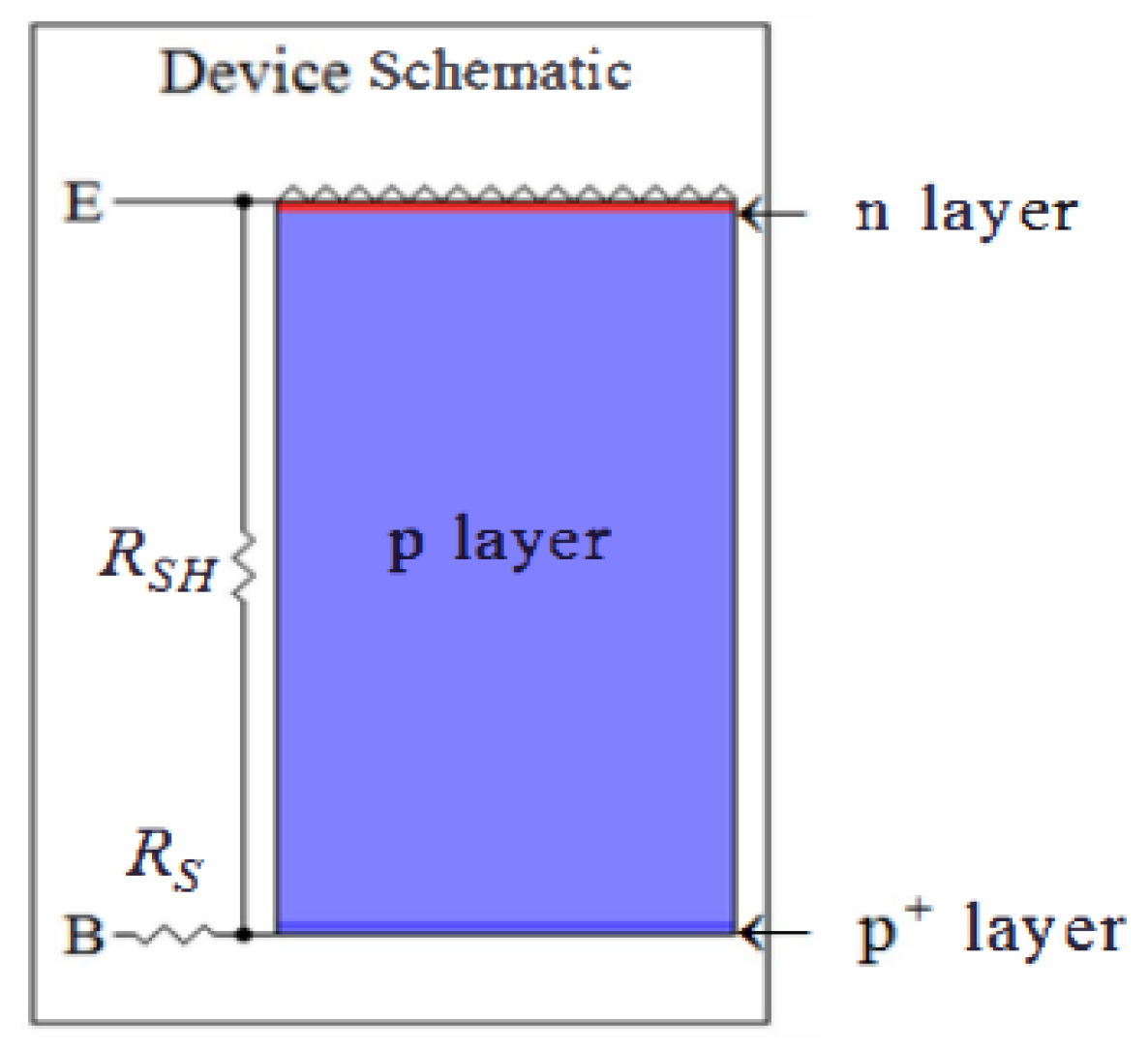
2. Solar Cell Modelling Using PC1D

The solar cell electrical and optical behaviour with the change in emitter configurations, such as the sheet resistance and emitter doping concentration was studied using the P C 1 D software. The advantage of using numerical modelling tools, such as P C 1 D , in order to optimize the emitter configurations is that the use of these simulation tools reduces the cost, time, and efforts required to analyse the impact of the change in configuration of the solar cells. The P C 1 D tool considers a basic schematic of the solar cell as illustrated in Figure 2.
P C 1 D is one of the commonly used numerical modelling simulation tools used for crystalline Si ( c - S 1 ) solar cell device simulations. The numerical model incorporated within the P C 1 D software package represents the quasi-one-dimensional transportation of electrons and holes of a semiconductor material (Solar cells). Equations (1)–(7) illustrate the basic governing equations of the numerical model used in the P C 1 D software package. A similar models have been created to use the model of a silicon cell, and P C 1 D is used for optimizing various process parameters, including the ARC coating layer properties [5], etc.
J n = μ n · n · E F n
J p = μ p · p · E F p
J n and J p represent the current densities of the electrons and the holes, respectively. μ n and μ p are the mobility of the electron and holes, and n and p are the electron and hole density, respectively. The E F n and E F p are the diffusion coefficients, which represent the difference in the electron and hole quasi-Fermi energies E F n and E F p . Equations (1) and (2) are the numerical representation of the current densities.
n t = · J n q + G L U n
p t = · J p q + G L U p
Δ 2 ϕ = q ϵ n p + N a c c N d o n +
Inferences from the law of conservation of charge or the continuity equation lead to the formulation of Equations (3) and (4). where G L and U n are generation rate and recombination rate, respectively. Equation (5) represents Poisson’s equation for solving the electrostatic field problems in which N a c c and N d o n + are the acceptor and donor doping concentrations.
n = N C F 1 / 2 q ψ + V n q ϕ n , i + ln n i , 0 / N C k B T
p = N V F 1 / 2 q ψ + V p q ϕ p , i + ln n i , 0 / N V k B T
In (6) and (7), the effective density of states in the conduction and valence bands are represented as N c and N v , respectively, to describe the type of material used, Fermi–Dirac statistics directly related to the band edges. The finite element approach is used to solve the three basic equations that assist in simulating the solar cell behaviours using the P C 1 D modelling tool. The optimization of the process parameters using the P C 1 D simulation tool is widely studied in the literature, but the proposed research aims to optimise the design process characteristics of the effective doping concentration of the emitter used in the fabrication of the c-Si solar cells. Finally, the efficiency of c-Si solar cells is calculated using the following Equation (8).
η = P max I in = J mpp V mpp I in = J SC V OC F F I in
where η represents the efficiency of the solar cell, which is calculated using P max , I in , J mpp , V mpp , J SC , V OC and F F that indicates the maximum power, incident power, current at maximum power point, voltage at maximum power point, saturation current density, open circuit voltage, and fill factor, respectively. PC1D is limited to one-dimensional modelling. The doping profiles are approximated by error functions that give the best fit to the experimental data. However, these might not possess the same shape of the doping profiles obtained experimentally. Particularly, the peak surface concentrations for the simulated profiles are overestimated, which might reduce the cell potential.
The concentration of the electrons and holes in the silicon layer of the c-Si solar cell is modified and optimized by the process of doping. The doping concentration and the type of doping (shallow or deep) influences the electrical conductivity of the semiconductor material making the solar cell more efficient. The electrical conductivity of the c-Si solar cell depends mainly on the parameters, such as the doping concentration and the mobility of the electrons and holes in the semiconductor region of the solar cell. Figure 3 illustrates the different dopant concentration levels of the c-Si solar cells, and in this paper, we critically test the heavy doping region with varying sheet resistance.
In this simulation, we considered the uniform distribution across the wafers. A detailed overview of the assumptions considered and the experimental procedure for the simulation is highlighted in the following section.

3. Simulation of c-Si Solar Cell

In this present study, we considered the actual device configuration for optimizing the n + p p + solar cell by P C 1 D simulation. Numerous simulations were performed to study the impact of different parameters on the solar cell device performance. The solar cell parameters used for the simulation is depicted in Table 1. The base resistance (0.015 Ω ), internal conductor (0.3 S), and light intensity (0.1 W/cm 2 ) were kept constant during simulation, as the doping concentration and the sheet resistance were varied, and the cell performance was evaluated. As recommended by Bremner et al., the A M 1.5 G spectrum was used in the modelling of the c-Si solar cell [16].
For detailed analysis of the recombination in an emitter, we used the E D N A 2 simulation program [17]. This simulator can determine the following factors: (i) recombination that occurs in both emitter as well as back surface field (BSF) (ii) emitter saturation current density ( J 0 e ) and (iii) internal quantum efficiency (IQE) for the chosen dopant profile. In the present study, we applied the following models: Trupke radiative recombination [18], Ritcher Auger recombination [19], Shockley–Read–Hall (SRH) recombination [20] to calculate the effective surface recombination velocity (as 1× 10 4 cm/s).
Mobility and band gap were modelled using Klaassen’s for mobility [21], Passler’s for intrinsic band gap [22], Sentaurus’s for density of states model [23], Altermatt’s for dopant ionization model [24], Schenk’s model for band gap narrowing [25] and Fermi–Dirac statistics [26]. With the above said models and error functions (ERFC), the n + (phosphorous) doping profiles with maximum doping concentration of 1 × 10 20 cm 3 were calibrated. Initially, we analysed the c-Si solar cell’s performance with the change in sheet resistance and later with the different doping profile and the results of the these observations are deliberately discussed in the following section.

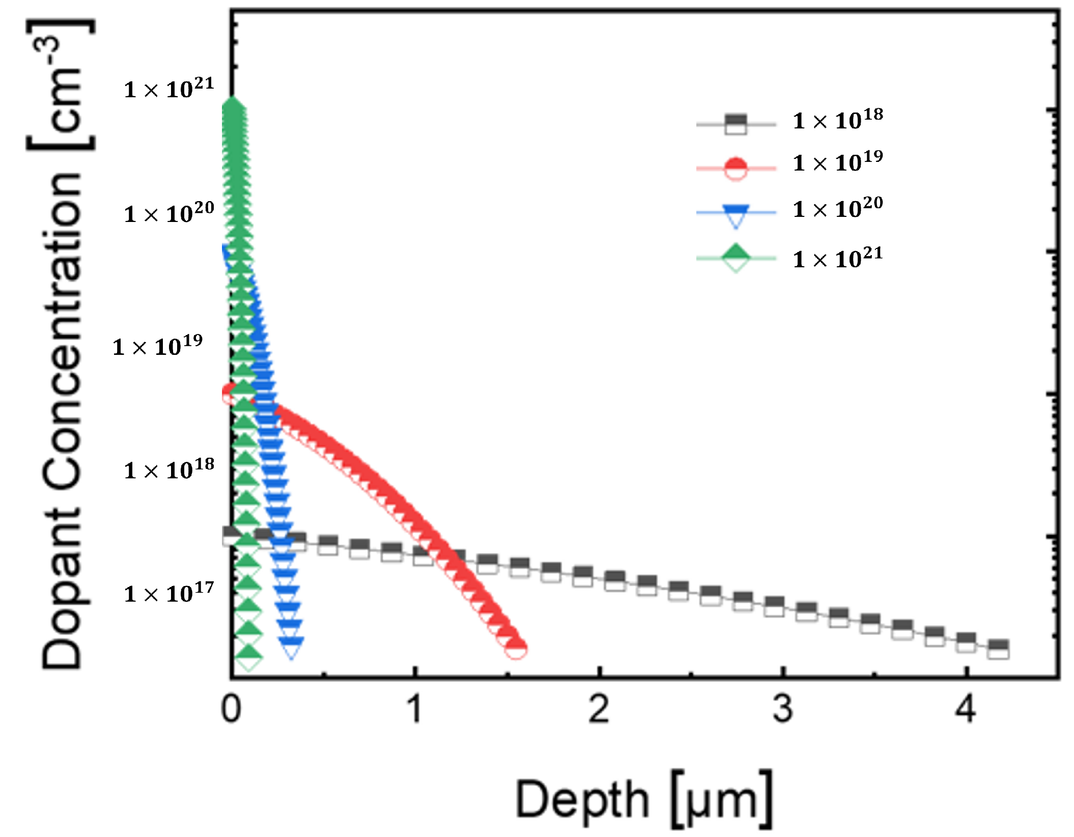
4. Results and Discussion

The emitter ( n + ) sheet resistance R s h e e t is one of the imperative parameters that can influence the recombination losses at the front side of the solar cell. Therefore, the improvement in the saturation current density at the emitter, surface, and contact is a concern to be aware of when increasing the sheet resistance of the emitter. In order to study the impact of the emitter sheet resistance R s h e e t on the efficiency of the solar cell, we fixed the doping concentration as 1 × 10 20 cm 3 and observed the change in possible junction depth as depicted in Figure 4.
It is clear from the observations that the lower the R s h e e t , the deeper the junction. To achieve a R s h e e t of 50 Ω /sq, the junction depth should be 0.59 μ m. Higher R s h e e t of 130 Ω /sq was obtained for the shallow junction depth of 0.21 μ m. The high R s h e e t at the emitter are benign for low saturation current density at the front.
Figure 5 displays the various current and voltage (I–V) parameters, such as ( J s c , V o c , FF, and efficiency) of Si solar cell simulated using P C 1 D against the R s h e e t . Figure 5 shows an improvement in J s c and slight variation in the V o c with respect to the variation in the R s h e e t . It is clear that a shallow emitter junction is preferable for highly-efficient solar cells. As the junction depth becomes shallower, the current density increases and, hence, the fill factor. A gain in J s c by 0.6 mA/cm 2 and V o c by 3 mV was observed for the high R s h e e t .
This increase in R s h e e t , lowers the Auger recombination and enhances the quantum efficiency in the short wavelength range. The increase in V o c with increase in R s h e e t can be attributed to the decrease in front surface doping concentration that contributes to the reduced Auger recombination. It is well known that the V o c is inversely proportional to the reverse saturation current density; thus, the V o c increases with increase in R s h e e t . Hence, the current photovoltaic industry utilize >90 Ω /sq in its homogeneously diffused n+ emitters and is expected to increase >130 Ω /sq by 2030 [27], which is evident from the results observed in the simulation.
Though the lightly doped emitter with R s h e e t of 130 Ω /sq yielded a high V o c , in actual cell fabrication process there would be a drop in V o c after front grid metallization. Screen-printed A g pastes with lower surface doping concentration can significantly reduce this V o c loss. However, with lightly doped emitters, the metal recombination losses increase due to the etching nature of the A g pastes. This limits the cell efficiency gain in experimentally fabricated cells [28]. To overcome this limitation, a dual print approach i.e., printing bus bars with less aggressive pastes and then printing fine metal fingers might reduce the metallization-induced recombination losses and in turn increase the conversion efficiency of the Si solar cells.
The doping concentration was fixed, and the change in junction depth was observed. Quantum Efficiency (QE) is one of the most crucial parameter of a solar cell. It is the ratio of number of carriers collected by the solar cell to the number of incident photons for a given wavelength [29]. The increase in quantum efficiency indicates the improvement in carrier collection. Thus, QE reveals the contribution of photons with different wavelengths towards J s c .
IQE is another parameter utilized to characterize the quality of solar cells in the short wavelength range of 300–500 nm. Most of the light in the blue wavelength region is absorbed by the emitter. The increase in J s c for the shallow junction depth (130 Ω /sq) is attributed towards enhancement in IQE. Figure 6 depicts the simulated internal quantum efficiency with respect to the variation in R s h e e t . The spectral response also determines/indicates the recombination rate on the frontal surface of c-Si solar cell, which is closely related to the junction depth.
The decrease in total J 0 e contributes to the increase in R s h e e t . Table 2 shows the split of the recombination mechanism predominant in each R s h e e t . It is well known that three different kind of recombination occurs in semiconductor. The radiative recombination is almost negligible for all the R s h e e t as the emitted photon has energy, such as at the band gap, and is therefore weakly absorbed.
The Auger recombination decreases with higher R s h e e t . Auger recombination is vital at high carrier concentrations, which is caused by either heavy doping or high level injection at concentrated sunlight. Auger recombination limits the lifetime and cell efficiency. The SRH recombination increases slightly with an increase in R s h e e t .
By fixing the R s h e e t , the emitter dopant concentration was varied as depicted in Figure 7. The heavy doping concentration (1× 10 18 cm 3 ) and shallow doping concentration (1 × 10 21 cm 3 ) ended in deeper and shallow junction, respectively. Though lightly doped emitter with high surface concentration is expected to have a good emitter properties (low J 0 e , better blue response), the junction depth is too shallow. This shallow junction induced high shunt resistance and series resistance, thereby, leading to poor solar cell performance. Similarly, the heavily doped emitter ended in a deeper junction, which decreased the series resistance, and thus a better FF was due to a low surface dopant concentration; however, J s c and V o c dropped due to poor surface passivation with high dopant concentration. Thus, a doping concentration in the order of 1 × 10 20 cm 3 with good junction depth is preferred.

5. Conclusions

The effect of the emitter sheet resistance on the performance of a silicon solar cell was studied. The phosphorus dopant profiles with a peak dopant concentration of 1 × 10 20 cm 3 were fixed, and the sheet resistance was varied using E D N A 2 simulation. The R s h e e t was varied from 50 to 130 Ω /sq. The results show that the emitter saturation current density decreased from 66.52 to 36.82 fA/cm 2 with an increase in the sheet resistance during n + (phosphorus) diffusion.
This decrease in the values of J 0 e is attributed to the decrease in Auger recombination. The internal quantum efficiency increased from 89.6 % to 97.5 % for the corresponding surge in sheet resistance. The short circuit density and open circuit voltage increased by 0.6 mA/cm 2 and 3 mV, respectively, for the 130 Ω /sq sheet resistance, which showed the highest efficiency of 20.6 % . However, metallization-induced recombination losses occurred on the phosphorus-diffused emitters with varying surface doping concentrations and junction depths. Thus, in the future, we aim to study the metallization-induced recombination on the various doping profiles, which will be helpful for our fellow researchers in the PV industry for improving device performance.

Author Contributions

Conceptualization, M.S. (Maruthamuthu Subramanian), B.N. and V.R.M.R.; methodology, B.N., M.S. (Maruthamuthu Subramanian), M.S. (Mehdi Seyedmahmoudian) and A.S.; software, A.R., G.S.T., E.J. and V.S.B.; validation, M.S. (Mehdi Seyedmahmoudian), A.S., S.M., E.J. and G.S.T.; formal analysis, G.S.T., A.R. and V.S.B.; investigation, M.S. (Maruthamuthu Subramanian), B.N. and V.R.M.R.; resources, M.S. (Mehdi Seyedmahmoudian), A.S., S.M., E.J. and V.R.M.R.; data curation, G.S.T., E.J. and M.S. (Mehdi Seyedmahmoudian); writing—original draft preparation, M.S. (Maruthamuthu Subramanian), B.N., A.R., G.S.T., E.J. and V.S.B.; writing—review and editing, E.J., M.S. (Maruthamuthu Subramanian), A.S. and S.M.; visualization, G.S.T., E.J., A.R. and V.S.B. All authors have read and agreed to the published version of the manuscript.

Funding

This research received no external funding.

Institutional Review Board Statement

Not applicable.

Informed Consent Statement

Not applicable.

Data Availability Statement

Not applicable.

Conflicts of Interest

The authors declare no conflict of interest.

References

  1. Madeti, S.R.; Singh, S. Monitoring system for photovoltaic plants: A review. Renew. Sustain. Energy Rev. 2017, 67, 1180–1207. [Google Scholar] [CrossRef]
  2. Rezk, H.; Tyukhov, I.; Al-Dhaifallah, M.; Tikhonov, A. Performance of data acquisition system for monitoring PV system parameters. Measurement 2017, 104, 204–211. [Google Scholar] [CrossRef]
  3. Panwar, N.; Kaushik, S.; Kothari, S. Role of renewable energy sources in environmental protection: A review. Renew. Sustain. Energy Rev. 2011, 15, 1513–1524. [Google Scholar] [CrossRef]
  4. Matthias, L. Total primary Energy supply from sunlight. Retrieved April 2006, 6, 2012. [Google Scholar]
  5. Thirunavukkarasu, G.S.; Seyedmahmoudian, M.; Chandran, J.; Stojcevski, A.; Subramanian, M.; Marnadu, R.; Alfaify, S.; Shkir, M. Optimization of Mono-Crystalline Silicon Solar Cell Devices Using PC1D Simulation. Energies 2021, 14, 4986. [Google Scholar] [CrossRef]
  6. Battaglia, C.; Cuevas, A.; De Wolf, S. High-efficiency crystalline silicon solar cells: Status and perspectives. Energy Environ. Sci. 2016, 9, 1552–1576. [Google Scholar] [CrossRef] [Green Version]
  7. Stem, N.; Cid, M. Physical limitations for homogeneous and highly doped n-type emitter monocrystalline silicon solar cells. Solid-State Electron. 2004, 48, 197–205. [Google Scholar] [CrossRef]
  8. Franklin, E.; Fong, K.; McIntosh, K.; Fell, A.; Blakers, A.; Kho, T.; Walter, D.; Wang, D.; Zin, N.; Stocks, M.; et al. Design, fabrication and characterisation of a 24.4% efficient interdigitated back contact solar cell. Prog. Photovolt. Res. Appl. 2016, 24, 411–427. [Google Scholar] [CrossRef]
  9. Steinkemper, H.; Hermle, M.; Glunz, S.W. Comprehensive simulation study of industrially relevant silicon solar cell architectures for an optimal material parameter choice. Prog. Photovolt. Res. Appl. 2016, 24, 1319–1331. [Google Scholar] [CrossRef]
  10. Doshi, P.; Mejia, J.; Tate, K.; Kamra, S.; Rohatgi, A.; Narayanan, S.; Singh, R. High-efficiency silicon solar cells by low-cost rapid thermal processing, screen printing, and plasma-enhanced chemical vapor deposition. In Proceedings of the Conference Record of the Twenty Fifth IEEE Photovoltaic Specialists Conference, Washington, DC, USA, 13 May 1996; pp. 421–424. [Google Scholar]
  11. Oh, J.; Yuan, H.C.; Branz, H.M. An 18.2%-efficient black-silicon solar cell achieved through control of carrier recombination in nanostructures. Nat. Nanotechnol. 2012, 7, 743–748. [Google Scholar] [CrossRef]
  12. Clugston, D.A.; Basore, P.A. PC1D version 5: 32-bit solar cell modeling on personal computers. In Proceedings of the Conference Record of the Twenty Sixth IEEE Photovoltaic Specialists Conference-1997, Anaheim, CA, USA, 29 September–3 October 1997; pp. 207–210. [Google Scholar]
  13. Fell, A.; McIntosh, K.R.; Altermatt, P.P.; Janssen, G.J.; Stangl, R.; Ho-Baillie, A.; Steinkemper, H.; Greulich, J.; Müller, M.; Min, B.; et al. Input parameters for the simulation of silicon solar cells in 2014. IEEE J. Photovolt. 2015, 5, 1250–1263. [Google Scholar] [CrossRef] [Green Version]
  14. Kim, B.; Park, C.; Balaji, N.; Lee, Y.; Song, K.; Jung, W.; Choi, J.; Ju, M.; Lee, J.; Lee, H.; et al. Doping Profile Effect of Shallow Emitter Junction in Selective Emitter c-Si Solar Cell with Reactive Ion Etching Etch Back Process. J. Comput. Theor. Nanosci. 2013, 10, 1779–1783. [Google Scholar] [CrossRef]
  15. Park, C.; Ahn, S.; Kim, B.; Song, K.; Choi, J.; Balaji, N.; Ju, M.; Lee, H.; Yi, J. An Analysis and Optimization of Selective Emitter with Etched-Back Structure of Crystalline Silicon Solar Cells Using TCAD Simulation. J. Comput. Theor. Nanosci. 2013, 10, 1772–1778. [Google Scholar] [CrossRef]
  16. Bremner, S.; Levy, M.; Honsberg, C.B. Analysis of tandem solar cell efficiencies under AM1. 5G spectrum using a rapid flux calculation method. Prog. Photovolt. Res. Appl. 2008, 16, 225–233. [Google Scholar] [CrossRef]
  17. Fell, A.; McIntosh, K.R.; Abbott, M.; Walter, D. Quokka version 2: Selective surface doping, luminescence modeling and data fitting. In Proceedings of the 23rd International Photovoltaic Science and Engineering Conference 2013, Taipei, Taiwan, 28 October–1 November 2013. [Google Scholar]
  18. Trupke, T.; Green, M.A.; Würfel, P.; Altermatt, P.; Wang, A.; Zhao, J.; Corkish, R. Temperature dependence of the radiative recombination coefficient of intrinsic crystalline silicon. J. Appl. Phys. 2003, 94, 4930–4937. [Google Scholar] [CrossRef] [Green Version]
  19. Richter, A.; Glunz, S.W.; Werner, F.; Schmidt, J.; Cuevas, A. Improved quantitative description of Auger recombination in crystalline silicon. Phys. Rev. B 2012, 86, 165202. [Google Scholar] [CrossRef] [Green Version]
  20. Maeda, T.; Narita, T.; Ueda, H.; Kanechika, M.; Uesugi, T.; Kachi, T.; Kimoto, T.; Horita, M.; Suda, J. Shockley–Read–Hall lifetime in homoepitaxial p-GaN extracted from recombination current in GaN p–n+ junction diodes. Jpn. J. Appl. Phys. 2019, 58, SCCB14. [Google Scholar] [CrossRef]
  21. Klaassen, D. A unified mobility model for device simulation—I. Model equations and concentration dependence. Solid-State Electron. 1992, 35, 953–959. [Google Scholar] [CrossRef]
  22. Pässler, R. Semi-empirical descriptions of temperature dependences of band gaps in semiconductors. Phys. Status Solidi b 2003, 236, 710–728. [Google Scholar] [CrossRef]
  23. Passeri, D.; Moscatelli, F.; Morozzi, A.; Bilei, G. Modeling of radiation damage effects in silicon detectors at high fluences HL-LHC with Sentaurus TCAD. Nucl. Instruments Methods Phys. Res. Sect. A Accel. Spectrometers Detect. Assoc. Equip. 2016, 824, 443–445. [Google Scholar] [CrossRef] [Green Version]
  24. Altermatt, P.; Schenk, A.; Heiser, G. A simulation model for the density of states and for incomplete ionization in crystalline silicon. I. Establishing the model in Si: P. J. Appl. Phys. 2006, 100, 113715. [Google Scholar] [CrossRef]
  25. Schenk, A. Finite-temperature full random-phase approximation model of band gap narrowing for silicon device simulation. J. Appl. Phys. 1998, 84, 3684–3695. [Google Scholar] [CrossRef]
  26. Dexter, D.; Seitz, F. Effects of dislocations on mobilities in semiconductors. Phys. Rev. 1952, 86, 964. [Google Scholar] [CrossRef]
  27. Fischer, M.; Woodhouse, M.; Herritsch, S.; Trube, J. International Technology Roadmap for Photovoltaic (ITRPV); Technical Report; VDMA: Frankfurt am Main, Germany, 2020. [Google Scholar]
  28. Shanmugam, V.; Khanna, A.; Basu, P.K.; Aberle, A.G.; Mueller, T.; Wong, J. Impact of the phosphorus emitter doping profile on metal contact recombination of silicon wafer solar cells. Sol. Energy Mater. Sol. Cells 2016, 147, 171–176. [Google Scholar] [CrossRef]
  29. Chander, S.; Purohit, A.; Nehra, A.; Nehra, S.; Dhaka, M. A study on spectral response and external quantum efficiency of mono-crystalline silicon solar cell. Int. J. Renew. Energy Res. (IJRER) 2015, 5, 41–44. [Google Scholar]
Figure 1. Structure of a c-Si solar cell [5].
Crystals 12 00244 g001
Figure 2. Schematic of the solar cell model [5].
Crystals 12 00244 g002
Figure 3. Dopant concentration levels [5].
Crystals 12 00244 g003
Figure 4. Variation in the R s h e e t by fixing the emitter dopant concentration 1 × 10 20 cm 3 .
Crystals 12 00244 g004
Figure 5. I–V characteristics as a function of R s h e e t .
Crystals 12 00244 g005
Figure 6. Simulated internal quantum efficiency as a function of R s h e e t .
Crystals 12 00244 g006
Figure 7. Variation in the emitter dopant concentration by fixing R s h e e t .
Crystals 12 00244 g007
Table 1. Unique characteristics of each appliance used in the simulations [5].
CharacteristicsValue
Device area 244.32 cm 2
Front/rear surface texture depth54.74 /3  μ m
Front/Rear surface coating S i N x 80 nm − n = 2.03
Internal optical reflectanceEnabled
Thickness180 μ m
Intrinsic concentration ni @ 300 K 1 × 10 10 cm 3
n + diffusion 1 × 10 20 cm 3
p + diffusion 3 × 10 18 cm 3
Front and rear SRV10,000 cm/s
Bulk recombination100 μ s
Temperature 25 °C
Table 2. Impact of variation in the emitter saturation current densities as a function of R s h e e t .
R sheet  
[Ω/sq.]
IQE E
 [%]
J 0 e , radiative
[fA/cm 2 ]
J 0 e , Auger
[fA/cm 2 ]
J 0 e , SRH
[fA/cm 2 ]
J 0 e , total
[fA/cm 2 ]
5089.60.0352.5313.9666.52
7093.70.0238.9714.653.59
9095.80.0230.6514.9245.59
11096.90.0125.3515.0940.45
13097.50.0121.6215.1936.82
Publisher’s Note: MDPI stays neutral with regard to jurisdictional claims in published maps and institutional affiliations.

