Article

Application of the Alexander–Haasen Model for Thermally Stimulated Dislocation Generation in FZ Silicon Crystals

1
Institute of Numerical Modelling, University of Latvia, Jelgavas Street 3, LV-1004 Riga, Latvia
2
Leibniz-Institut für Kristallzüchtung, Max-Born-Str. 2, 12489 Berlin, Germany
*
Author to whom correspondence should be addressed.
Crystals 2022, 12(2), 174; https://doi.org/10.3390/cryst12020174
Submission received: 31 December 2021 / Revised: 14 January 2022 / Accepted: 19 January 2022 / Published: 25 January 2022
(This article belongs to the Section Crystal Engineering)

Abstract

:
Numerical simulations of the transient temperature field and dislocation density distribution for a recently published silicon crystal heating experiment were carried out. Low- and high-frequency modelling approaches for heat induction were introduced and shown to yield similar results. The calculated temperature field was in very good agreement with the experiment. To better explain the experimentally observed dislocation distribution, the Alexander–Haasen model was extended with a critical stress threshold below which no dislocation multiplication occurs. The results are compared with the experiment, and some remaining shortcomings in the model are discussed.

1. Introduction

Dislocation-free silicon (Si) single crystals are grown with the Czochralski (CZ) and Floating-Zone (FZ) methods. The occurrence of dislocations is detrimental to process yield and needs to be avoided. Furthermore, in other growth processes, for solar Si in particular, dislocation density and distribution are important quality factors influencing many practically relevant material parameters such as the minority carrier lifetime.
In FZ and CZ processes, the initial dislocations are generated due to high temperature gradients arising during the contact of the crystalline seed with the melt. These are eliminated using the Dash technique—by growing a long, thin neck until dislocations terminate at the crystal surface by the climb mechanism [1]. Recent attempts to develop new techniques without the Dash neck, such as the modified FZ method, have shown that in cases using large-area seeds, the dislocations always occur at high temperatures above 1200 ° C [2,3]. In this case, dislocation generation is believed to be caused primarily by high thermal stresses. By adjusting the temperature gradients, the stress level and the final dislocation density in the crystal can be lowered [4].
To explain various experimental observations, early mathematical models in the literature proposed a simplified criterion—the critical resolved shear stress (CRSS) [5,6]. The elastic thermal stress field is calculated, and, if it is lower than CRSS, no dislocations will be generated. Otherwise, the dislocation density is proportional to the excess stress, which is the difference between the calculated stress and the CRSS. This model is only qualitative and does not explain why dislocation-free CZ and FZ crystals can be grown with calculated stresses exceeding the CRSS at least by an order of magnitude [7].
A quantitative model for the dislocation density proposed in [8] is known as the Alexander–Haasen (AH) model. It describes dislocation multiplication but not generation, and it is a local model, meaning that the multiplication rate does not depend on the neighbouring dislocation density values. The crystal initially must have a small non-zero dislocation density, which will increase (multiply) at different rates, depending on the stress level and the temperature. The AH model has been applied for Si and other semiconductor materials [9,10,11,12,13,14] and extended to multi-slip systems as the Haasen–Alexander–Sumino (HAS) model [15,16].
An advanced Alexander–Haasen model was used for the modelling of almost dislocation-free CZ and FZ Si crystals of different orientations in 3D [17]. The crystals were heated (not exceeding the melting point) and cooled down by controlling the temperature at monitoring points located on heaters. The calculated dislocation density distribution for the 111 crystal was in a worse agreement with the experiment than for the 100 crystal possibly due to the neglected dislocation propagation. However, since the whole crystal was heated, it is somewhat difficult to pinpoint at what conditions (temperature and stress) the dislocation generation was started.
To the best of the knowledge of the authors, no macroscopic dislocation density model (AH, HAS, or their modifications) allows to predict the generation of the first dislocations in an initially dislocation-free crystal. This model limitation implies that additional assumptions (e.g., non-zero initial dislocation density) have to be used for the numerical modelling of the CZ Si crystal growth [12], FZ Si crystal growth (no literature known), or other almost-dislocation-free setups [17]. Most existing numerical studies consider other materials or growth processes where the dislocations are always present, and their multiplication is well described by the AH model.
To better understand the origins of dislocation generation, an experiment by Rost et al. [18] related to the modified FZ process [2,3] was carried out. An as-grown FZ Si single crystal was heated by a high-frequency (HF) coil in a controlled manner up to different temperatures, depending on the position. No mechanical surface treatment was applied to avoid dislocation generation induced by surface defects. The time-dependent temperature of the crystal was measured, and a clearly defined initial dislocation generation at about 995 ° C was observed in later dislocation measurements. Thus, a set of experimental data is available for the validation of the mathematical models for temperature and dislocation density.
In the present study, the experiment [18] was analysed numerically using a new implementation of the AH model with the goal of validating the applicability for dislocation dynamics in FZ Si. A simplified volume distribution of the electromagnetic (EM) field from calculated surface values using the HF approach was introduced since the crystal diameter is comparable to the EM skin depth. The AH model, supplemented with a critical stress threshold, which imitates the effect of dislocation generation, was applied to describe the dislocation density dynamics. The results were compared with the experiment. Such temperature and dislocation density simulations for an as-grown Si crystal have not been published in the literature up to now. New solvers for the temperature, stress, and dislocation density are developed using open-source finite element library deal.II [19] and are freely available to all interested researchers as a new open-source solver package MACPLAS [20].

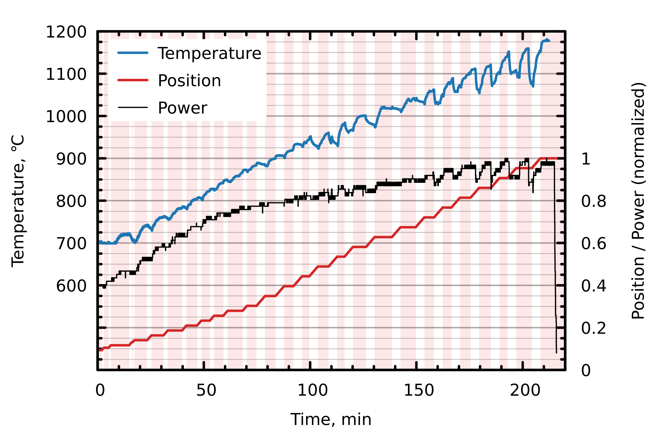
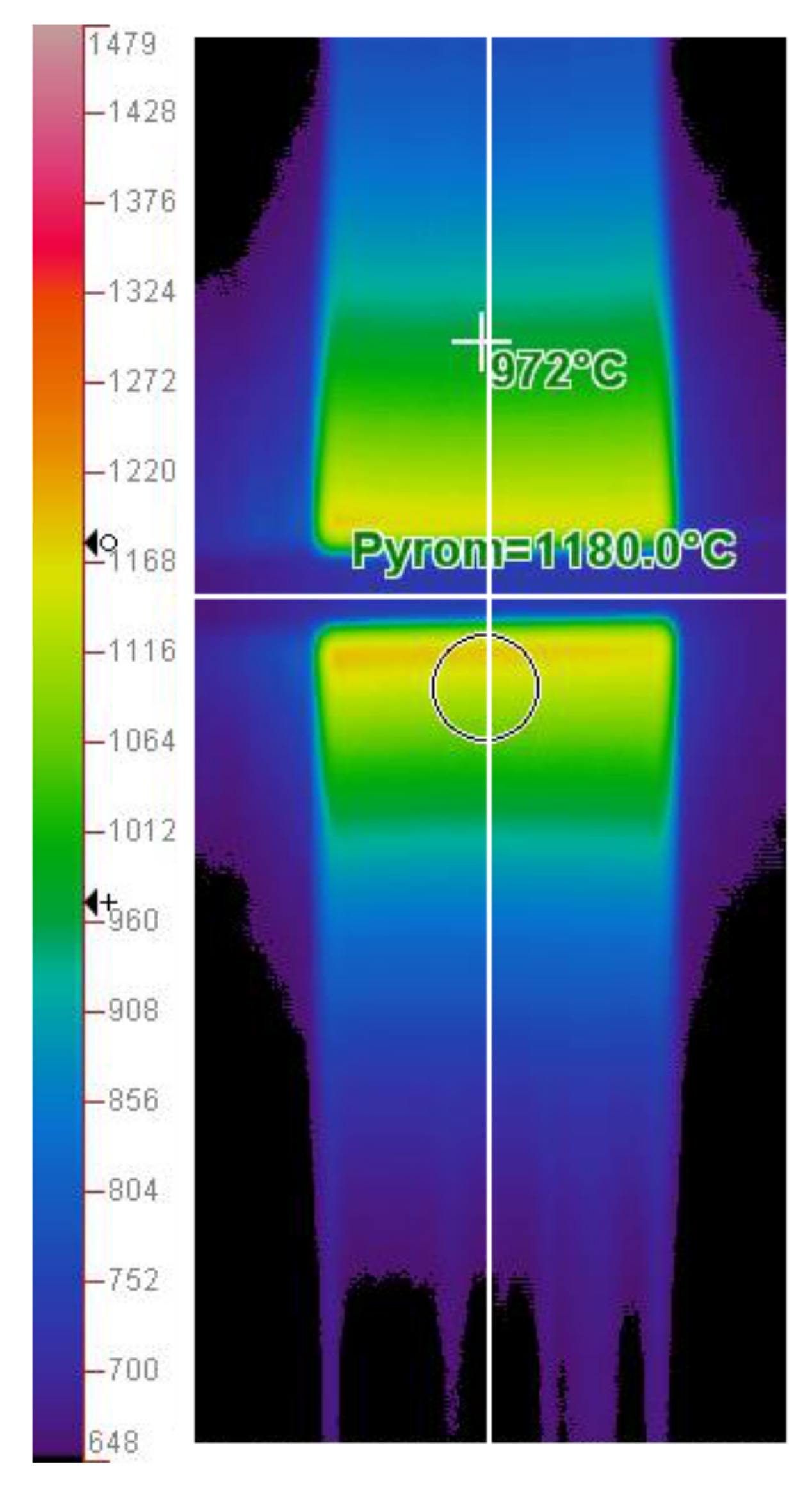
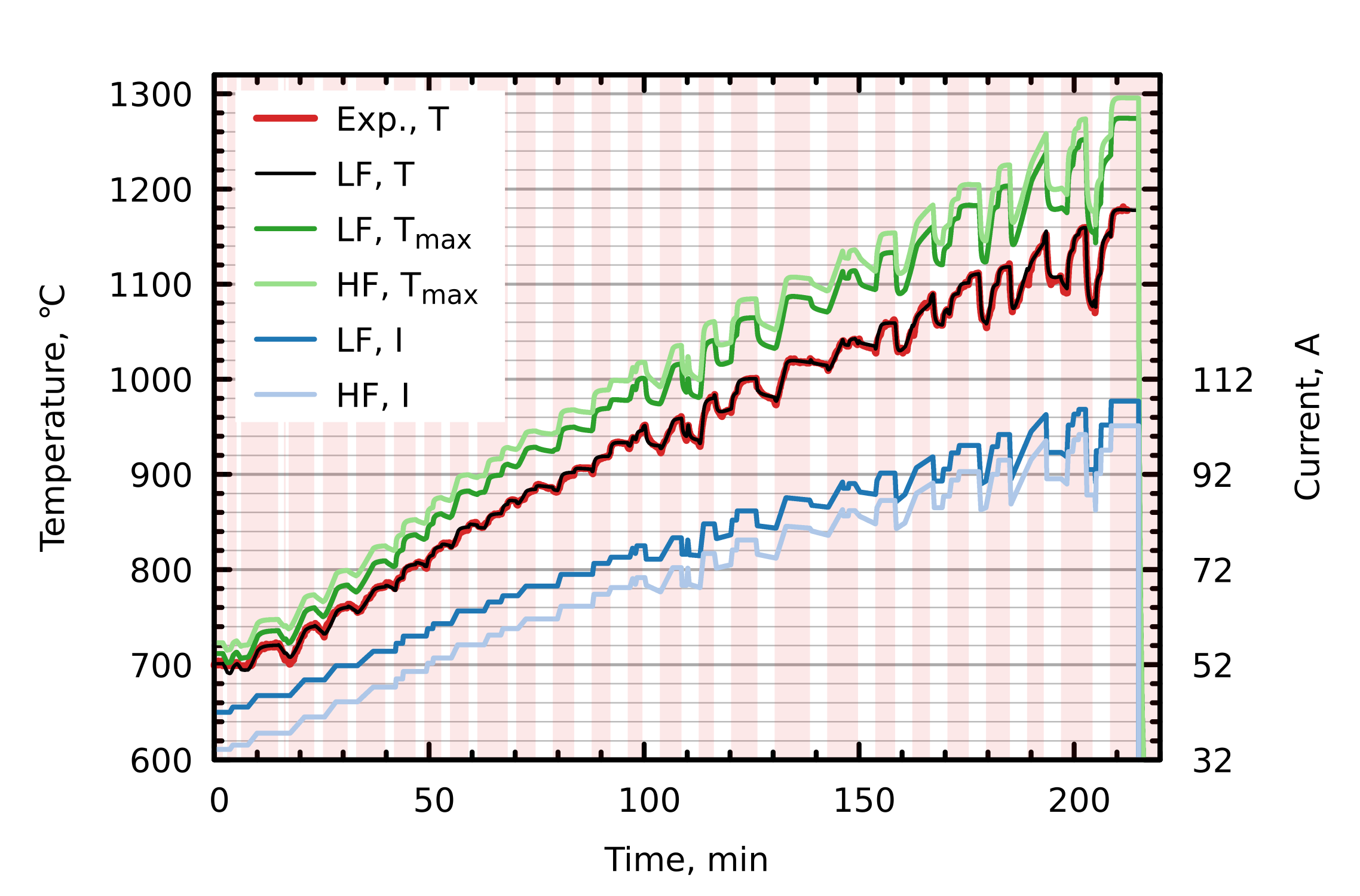
2. Description of Experiment

The experimental setup and obtained results are described in [18]; therefore, only a brief summary relevant for the numerical modelling is given in this section.
An as-grown 100 FZ Si single crystal with a diameter of 20 m m and a length of 480 m m was heated by an HF ( f = 2.715 M Hz ) inductor to increasing temperatures and shifted stepwise to different heating (i.e., crystal) positions. Temperature steps of about 20 K in the range of 700– 1180 ° C were applied; thus, the melting point of Si at T 0 = 1687   K = 1414   ° C was not exceeded. The temperature was monitored by a pyrometer with an integrated infrared camera (Advanced Energy, IMPAC ISR 6-TI Advanced), which measures the average temperature in a circular probe region; see Figure 1.
Since a ratio pyrometer (also known as two-color pyrometer) is used to measure the temperature, the obtained values are reliable because the temperature dependence of the emissivity ε ( T ) is taken into account automatically. A limitation, however, exists for the global temperature field because a constant emissivity is employed outside the probe region. This effect can be analysed by assuming ε T 4 = const from which the following estimation is derived:
T meas = T real ε ( T real ) ε ref 1 / 4 ,
where ε ref denotes the emissivity at the probe region; T meas —measured temperature at an arbitrary position; and T real —the actual temperature at this position. By using ε ( T ) from [21], one obtains from Equation (1) that pyrometer measurements of low temperatures 25 m m from the probe point below the inductor overestimate the real temperature by up to 50 ° C .
The crystal was shifted downwards relative to the inductor in 10 m m or 20 m m steps with a velocity V = 5   m m / min , following by prolonged stops to allow the temperature to reach the steady-state. In addition to the heating position change, the HF inductor power was increased over time to reach higher temperatures as depicted in Figure 2. The time t = 0 corresponds to the beginning of the stepwise heating, i.e., after the preheating.
A peculiar effect to note in Figure 2 is that both the measured temperature and the inductor power drop as the crystal starts to move. This effect is especially pronounced at high temperatures (above 1000 ° C ), when the temperature drop can reach 100 K . While the complete explanation is beyond the scope of the present article, a possible reason could be that the hot crystal at the heating position is replaced by a cooler region from above and, as a result of changed electrical conductivity and skin depth, the inductor-crystal impedance changes as well, leading to a reduction in induced power. It cannot be excluded that the power fluctuations are caused by the power control algorithm of the HF generator. From now on, it will be assumed that the temperature is affected by the prescribed time-dependent inductor power (in experiment) or current (in simulation).
Finally, after reaching the maximum temperature at t = 215 min , the inductor power was turned off. The crystal cool-down to room temperature was not analysed in the experiment.

3. Numerical Model

3.1. Heat Transfer

3.1.1. Temperature Field

The transient temperature equation is solved in the crystal:
ρ c p T t = · ( λ ( T ) T ) + q ˙ ,
where ρ is the density; c p —specific heat capacity; λ ( T ) —temperature-dependent thermal conductivity; and q ˙ —volumetric heat source. While 3D simulations are possible, a 2D (axisymmetric) model was employed in the present work to save computational resources. Another two reasons that justify the use of a 2D model is that (i) anisotropic material properties (elastic constants) have a weak influence on the results [13] and (ii) no clear deviation from axial symmetry in characterisation results was observed in the experiment [18].
The global heat transfer was not considered in the present study since only the temperature field in the crystal was of interest. Heat transfer between the crystal and parts of the FZ furnace is described by the following boundary condition, which was applied at the crystal side surface:
q = σ SB ε ( T 4 T amb 4 ) + h ( T T gas ) q EM ,
where q is the heat flux density; σ SB = 5.67 × 10 8 W / m 2 / K 4 is the Stefan–Boltzmann constant; ε —emissivity; T amb —ambient temperature; h—heat transfer coefficient; T gas —reference gas temperature; and q EM —surface heat sources. Three terms on the right-hand side of Equation (3) describe the effect of thermal radiation, convective gas cooling, and inductive heating, respectively.
The parameters T amb , T gas and h mainly affect the T ( z ) profile at low-temperature regions, while the maximum temperature was determined by the inductor current ( q EM term). Of particular importance are the convective heat losses, since for h = 0 the crystal temperature 30 m m below the inductor was ca. 40 K higher than in the experiment.
The view factors were not considered for the thermal radiation calculation; instead, the effect of the surroundings is described by a single parameter T amb . While this simplification was imprecise near the inductor, the corresponding view factors are likely to be small due to a small inductor height of 5 mm and a rather wide 3 m m gap between the crystal and the inductor (see Figure 9 of ref. [18]); therefore, no significant influence on the calculated temperature distribution was expected.

3.1.2. Heat Induction

Two different modes for numerical modelling of the heat induction are distinguished: HF and LF. In the HF (surface) mode, the induced power was applied as a temperature boundary condition at the crystal surface, Equation (3), and the volumetric heat source q ˙ in Equation (2) was set to zero. In the LF (volumetric) mode, the induced power was excluded from the boundary condition (3), and the spatially varying volumetric heat source q ˙ ( r , z ) was applied.
The HF EM field was calculated in 3D as described in [22]. The actual 3D inductor shape was used, and the results were azimuthally averaged and used in 2D temperature simulations as follows [21]:
q EM = i 2 π μ 0 f σ ,
where μ 0 = 4 ß × 10 7 H / m is the vacuum permeability; i—surface current density; f—inductor current frequency; and σ —electrical conductivity of the crystal. As i is proportional to the inductor current I, only one HF simulation with I = 1 A was needed to apply the time-dependent heating. For convenience, the crystal was not moved in the simulations, and the inductor was shifted instead (i.e., the distribution q EM ( z ) ).
The electrical conductivity of Si has a strong temperature dependence σ = σ ( T ) [23], which considerably affects the EM skin depth δ = 1 / π μ 0 f σ . The values of δ at 700 ° C and 1300 ° C were 7.3 m m and 2.0 m m , respectively, which are comparable to the crystal radius (10 m m ). Hence, the volumetric heat source should be considered for more precise results.
In principle, the LF EM field needs to be calculated at each time step to account for the spatially and temporally changing skin depth. In the present work, however, a simplified description of the LF EM field was employed, which saves computational resources yet captures the correct physics. The volume current density j was approximated with
j exp ( x δ ) ,
therefore, the volumetric heat source can be expressed as
q ˙ = j 2 σ = a exp ( 2 x δ ) ,
where x is the distance from the crystal surface, and the coefficient a is to be determined. The surface power density applied in the HF mode is [21]
q HF = lim L 0 L q ˙ x = a δ 2 ;
hence, a reasonable approximation for a is
a 2 q HF δ .
Strictly speaking, the skin depth was larger than the crystal radius far from the inductor where the crystal temperature was below 600 ° C . However, this model limitation can be neglected in simulations since, at such large distances from the inductor, q HF is practically vanishing.
It is relatively straightforward to derive an analytical expression for the temperature difference between HF and LF modes in 1D (see Appendix A). The value at the crystal surface is given by the equation
Δ T δ q HF 2 λ ,
which predicts that for q HF = 1 M W / m 2 (typical value at 1300 ° C for radial temperature gradient of 40 K / m m ), the maximum temperature in the LF mode is by ca. 45 K lower, compared to the HF mode. As will be demonstrated in Section 4.1, a difference of about 20 K was obtained in the 2D calculations, which took into account the axisymmetric geometry, non-homogeneous q HF ( z ) distribution, and temperature-dependent material properties. It was concluded that Equation (9) provides a reasonable estimation of Δ T and that the skin effect is important enough to be included in the simulations.

3.1.3. Equation Coupling

The numerical implementation of the heat transfer model is based on the open-source finite element library deal.II [19], which has been applied in the past for the modelling of transient temperature, stress, and point-defect fields [24]. The HF EM field was calculated beforehand using inductor current I = 1 A . During the simulations (each time step), the induced heat sources were scaled by I 2 and updated according to the temperature-dependent skin depth. Since both the temperature Equation (2) and the boundary condition (3) contain non-linearities, Newton’s method was applied. A direct solver was used for the system of linear equations. The developed temperature solver is available in the open-source library MACPLAS [20].

3.2. Dislocation Density Dynamics

3.2.1. Constitutive Equations

The Alexander–Haasen model [8] describes the time evolution of the dislocation density N m and plastic strain components ε i j c :
d N m d t = K v τ eff l N m ,
d ε i j c d t = b v N m 2 J 2 S i j ,
v = k 0 τ eff p exp ( Q k T ) ,
where v is the dislocation velocity; τ eff is the effective stress; b is the magnitude of Burgers vector; k = 8.617 × 10 5 e V / K is the Boltzmann constant; and Q is the activation energy (Peierls potential). J 2 = S i j S i j / 2 is the second invariant of the stress deviator S i j = σ i j δ i j σ k k / 3 . K, l, p, and k 0 are further material constants.
From a physical point of view, the multiplication law (10) together with the Orowan equation extended to a multiaxial stress state (11), assuming the crystal is isotropic [12], describe stress relaxation through plastic deformations and an increase in the dislocation density.
Using the Macaulay bracket notation x = max ( x , 0 ) 0 , the effective stress τ eff can be expressed as
τ eff = J 2 D N m τ crit ,
where D is the strain-hardening factor. An additional term— τ crit —was introduced, which is the critical stress for multiplication of dislocations. τ crit is analogous to the drag stress τ d , which has been applied in the literature to describe the influence of impurity concentration [11,12]. In a sense, the new term incorporates a threshold for the dislocation generation into the AH model since d N m / d t = 0 for J 2 < D N m + τ crit . It is demonstrated in Section 4.2 that non-zero τ crit is needed to improve agreement with the experiment.
Non-zero initial dislocation density N 0 was assumed in this study since dislocation generation is not included in the AH model, only multiplication. Models that include the generation of the first dislocations have not been published in the literature to the best of the knowledge of the authors. The value of N 0 has a weak influence on the results as long as it is sufficiently low [12]. Typically, values of N 0 of at least two orders of magnitude smaller than the final dislocation density are recommended. Zero initial values of the plastic strain were used.

3.2.2. Plastic Stress

The isotropic stress model was selected since it is known from the literature [13] that the anisotropy of Si only slightly changes the results. The axisymmetric stress components were calculated according to the following equation:
( σ r r σ z z σ ϕ ϕ σ r z ) = ( ϕ χ χ 0 χ ϕ χ 0 χ χ ϕ 0 0 0 0 G ) ( ε r r ε r r T ε r r c ε z z ε z z T ε z z c ε ϕ ϕ ε ϕ ϕ T ε ϕ ϕ c ε r z ε r z c ) ,
where the quantities ϕ = E ( 1 ν ) / ( ( 1 + ν ) ( 1 2 ν ) ) , χ = E ν / ( ( 1 + ν ) ( 1 2 ν ) ) , and G = E / ( 2 ( 1 + ν ) ) (shear modulus) are functions of the Poisson’s ratio ν and Young’s modulus E; ε i j c is the plastic strain obtained by integrating Equation (11); ε i j is the total strain; and ε i j T is the thermal strain given by
ε i j T = T ref T δ i j α ( T ) d T = α ¯ ( T ) · ( T T ref ) δ i j ,
where δ i j is the Kronecker delta; α is the differential thermal expansion coefficient; and α ¯ is the averaged thermal expansion coefficient, which is defined as
α ¯ ( T ) = 1 T T ref T ref T α d T .
Purely elastic stress is calculated by Equation (14) if all plastic strain components are zero.

3.2.3. Equation Coupling

The equations for the dislocation density and stress components were solved in a sequential manner. This approach restricts the maximum allowed time step, but it is already limited by a relatively fast crystal velocity in the heat transfer simulations. Adaptive time-stepping is employed, which automatically reduces the time step during rapid dislocation multiplication. Additionally, to improve numerical accuracy, a linearized version of Equation (10) assuming constant stress was integrated analytically in a similar manner as in ref. [10]. The stress field was calculated via the finite element method using the same mesh and element order as for the temperature field. A direct solver was used for the system of linear equations. The developed stress and dislocation density solvers are available in the open-source library MACPLAS [20].

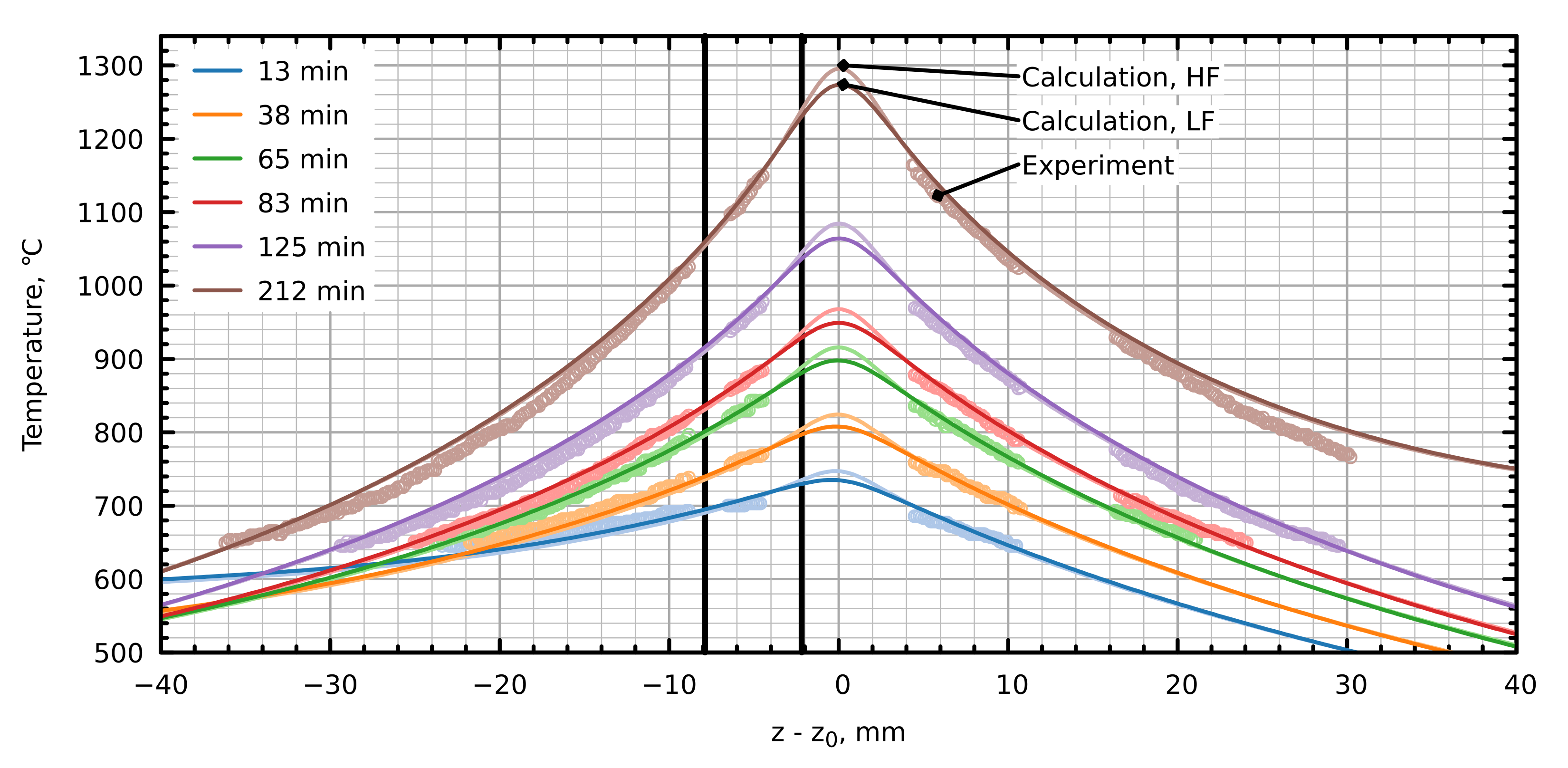
4. Results and Discussion

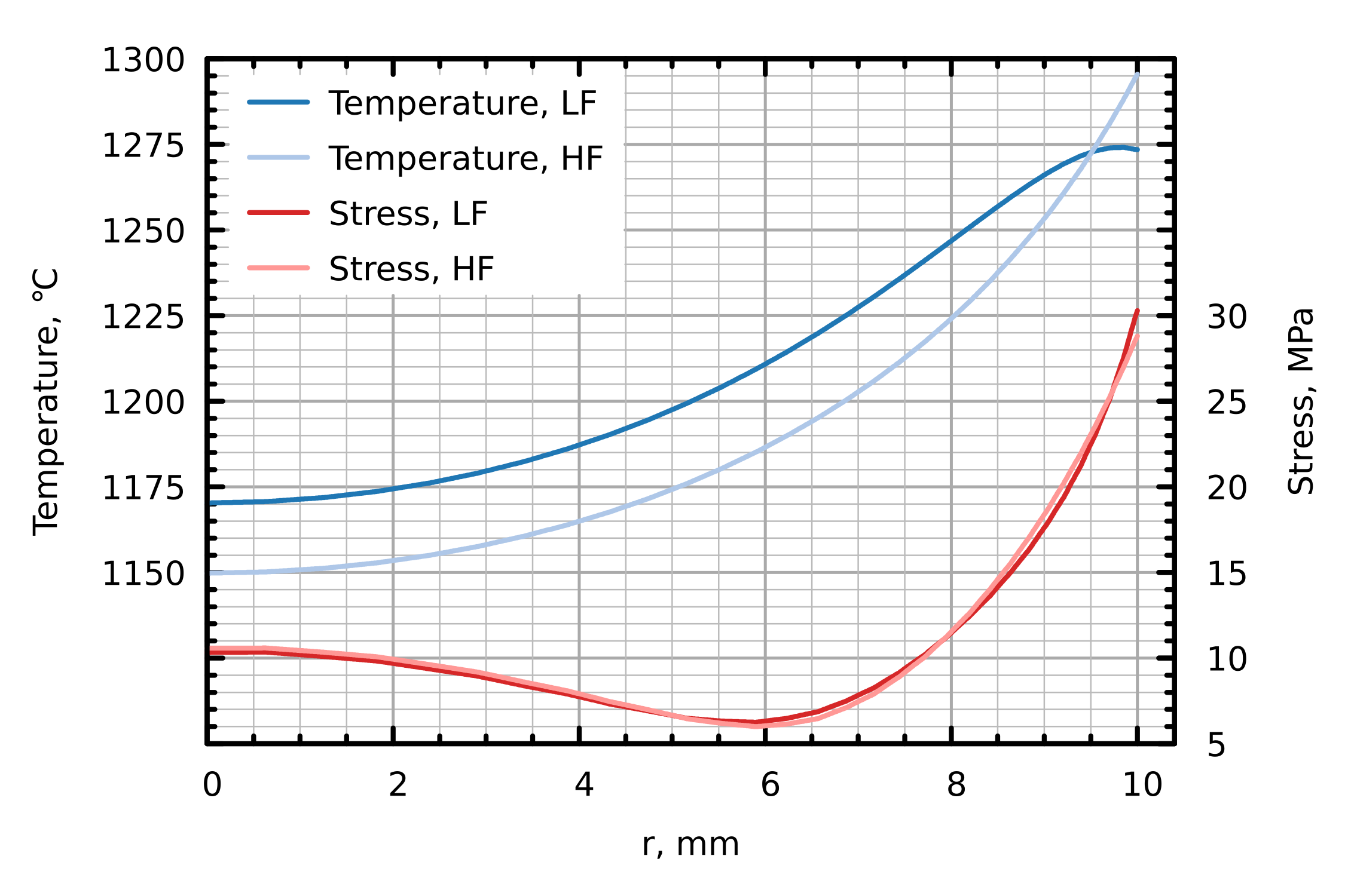
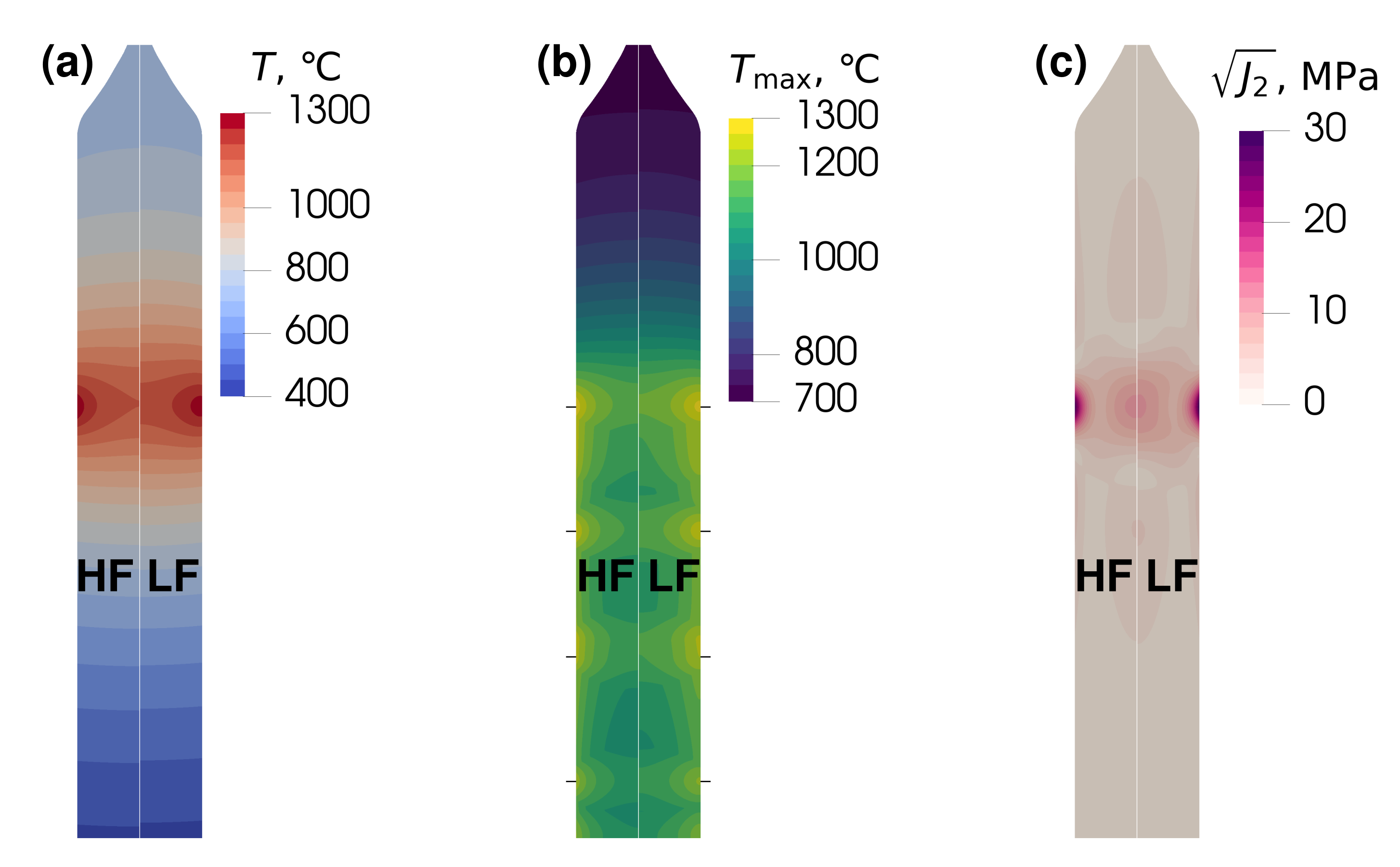
4.1. Heat Transfer and Elastic Stress

First, the temperature field was calculated to validate the heat transfer model. The following physical properties of solid Si were used: ρ = 2329 k g / m 3 and c p = 1000 J / k g / K [21]; the temperature-dependent electrical conductivity σ ( T ) , thermal conductivity λ ( T ) , and emissivity ε ( T ) are:
  • σ ( T ) = 100 · 10 4.247 2924 / T (in S / m ) [23];
  • λ ( T ) = 22 4.495 7.222 T / T 0 + 3.728 ( T / T 0 ) 2 (in W / m / K ) [21];
  • ε ( T ) = 0.46 · 1.39 , T < 0.593 T 0 0.46 · ( 1.96 0.96 T / T 0 ) , T 0.593 T 0 (dimensionless) [21].
The parameters for the convective cooling of crystal surface h = 10 W / m 2 / K and T gas = 300   K in the temperature boundary condition (3) were selected based on authors’ previous experience in the global heat transfer modelling during FZ Si crystal growth [25]. The same temperature value was used as the effective ambient temperature for thermal radiation: T amb = 300   K . Despite a much larger crystal diameter of 102 m m in ref. [25], the value of h used in the present work is justified based on two considerations: (i) the experiment took place in an inert gas atmosphere under similar conditions as the real FZ process, reaching comparably high temperatures; (ii) the crystal temperature 30 m m below the inductor was ca. 40 K higher than in the experiment when using h = 0 , while for h = 10 W / m 2 / K this discrepancy was practically eliminated.
A structured quadrilateral mesh capturing both the start- and end-cone shapes and consisting of about 15,000 cells was created using Gmsh [26]. The element size in the vertical direction was 0.5 m m . A non-uniform size distribution was applied for 15 cells in the radial direction with the minimum element size at the crystal surface of 0.3 m m . Second-order finite elements (nine-node quadrilaterals) were used, resulting in the total number of degrees of freedom for temperature of 61,000. The same discretization was used also for stress and dislocation density simulations (Section 4.2). A maximum time step of 1   s was imposed. The time step cannot be much larger due to highly localized EM power sources (profile full width at half maximum of about 4 m m ) and a relatively fast crystal movement velocity ( 5 m m / min ). The influence of the mesh size, finite element order, and the time step on the temperature field was checked by comparing the time-dependent maximum crystal temperature and the temperature at four probe points between simulations with different numerical settings and was found out to be very weak (below 0.5 K ).
The inductor current I was changed over time (Figure 3) in a similar manner as the experimentally applied power (Figure 2). Multiple iterations of manual I ( t ) adjustments were done for both the LF and HF modes to improve the agreement with the experimentally measured T ( t ) at chosen time instants. A higher current was required for the LF simulation due to a lower temperature at the crystal as explained in Section 3.1.2. For simplicity, the temperature integration over the measurement area was not done in simulations—the value at a single probe point corresponding to the measured temperature was used instead. This approach for a non-homogeneous temperature field could be justified by the vertical temperature profile T ( z ) which in the measurement area was close to linear.
As demonstrated in Figure 3, the simulations predicted the experiment very well with deviations less than 15 K . The observed temperature dropped as the crystal started to move (see Figure 2), which could only be obtained if the inductor current was reduced in the simulation. It is possible that the effective inductor current was indeed decreasing in the experiment due to the power control algorithm of the HF generator. However, additional experiments with current measurements would be required to validate this assumption.
Numerical simulations provide additional results that cannot be easily monitored in experiment—in particular, the area of maximum crystal temperature T max is hidden by the inductor. Figure 3 shows that T max is considerably higher (up to 100–120 K at the end of heating) than the measured temperature and exhibits the same drops as the crystal starts to move.
After the inductor power has been switched off, the crystal temperature drops (not shown fully in Figure 3) due to heat losses by thermal radiation and convection. This drop is so rapid that the maximum crystal temperature was below 500 ° C in just 2 min.
Since the exact inductor position z 0 (or distance between the measurement area and the inductor) is not easy to determine in the infrared images from the experiment—see Figure 1—it was done with the help of simulations—a symmetric T ( z z 0 ) distribution was obtained at t = 125 min , allowing to shift the experimental temperature profile vertically and obtain that the centre of the measurement area was 5.05 m m below the inductor ( z 0 corresponds to the horizontal line in Figure 1).
As shown in Figure 4, vertical temperature distributions for both the HF and LF simulations are in a good agreement with the experiment. As expected, the maximum crystal temperature in the HF mode was consistently higher than in the LF mode with the difference at the end of heating reaching ca. 20 K . The non-symmetry of the temperature field with respect to the inductor was primarily caused by different crystal lengths above and below the inductor at different times, not by transient effects.
Before simulations of the dislocation density dynamics, the elastic thermal stress was calculated using the following parameter values for the Poisson’s ratio ν , the temperature-dependent Young’s modulus E ( T ) , and the thermal expansion coefficient α ( T ) with T ref = 280   K in Equation (16):
  • ν = 0.25 (dimensionless) [9];
  • E ( T ) = 170 2.771 × 10 5 T 2 (in G Pa ) [9];
  • α ( T ) = 3.725 1 exp ( 5.88 × 10 3 ( T 124 ) ) + 5.548 × 10 4 T (in 10 6 / K ) [27].
Note that while the used FZ crystal was grown with a convex crystallization interface shape [18], the interface deflection is not relevant for the modelling of the considered experiment since the crystal was heated without melting.
A comparison between LF and HF modes given in Figure 5 reveals a noticeable temperature difference of ± 20 K both on the axis and at the crystal surface. The thermal stress, however, is almost the same with the values of ca. 10.5 M Pa on the axis, a minimum of 6 M Pa at r = 6 m m , and a maximum of 28.8 M Pa (LF) and 30.3 M Pa (HF) at the crystal surface. Hence, no major differences between LF and HF heat transfer models were expected in the dislocation density simulations.
Figure 6 shows 2D temperature and stress distributions at the end of heating. The instantaneous temperature field (Figure 6a) differs between LF and HF modes only in the vicinity of the inductor since in this region the majority of the Joulean power is induced. A specially post-processed field T max ( r , z ) = max T ( r , z , t ) is plotted in Figure 6b. It is interesting to observe the effects of alternating between crystal moving and stopping. Although the maximum crystal temperature was 1300 ° C , its upper part only became 700 ° C hot. Finally, Figure 6c depicts the thermal stress field at the end of heating, which was the highest at the crystal surface and roughly three times weaker near the axis. Due to the localized heating, the stress sharply drops as the distance from the inductor increases. At the heating position at time 119 min , which corresponds to the beginning of dislocation generation in the experiment [18] (not visible in Figure 6), the maximum crystal temperature was about 1016 ° C , and the stress J 2 was 25 M Pa (LF mode).

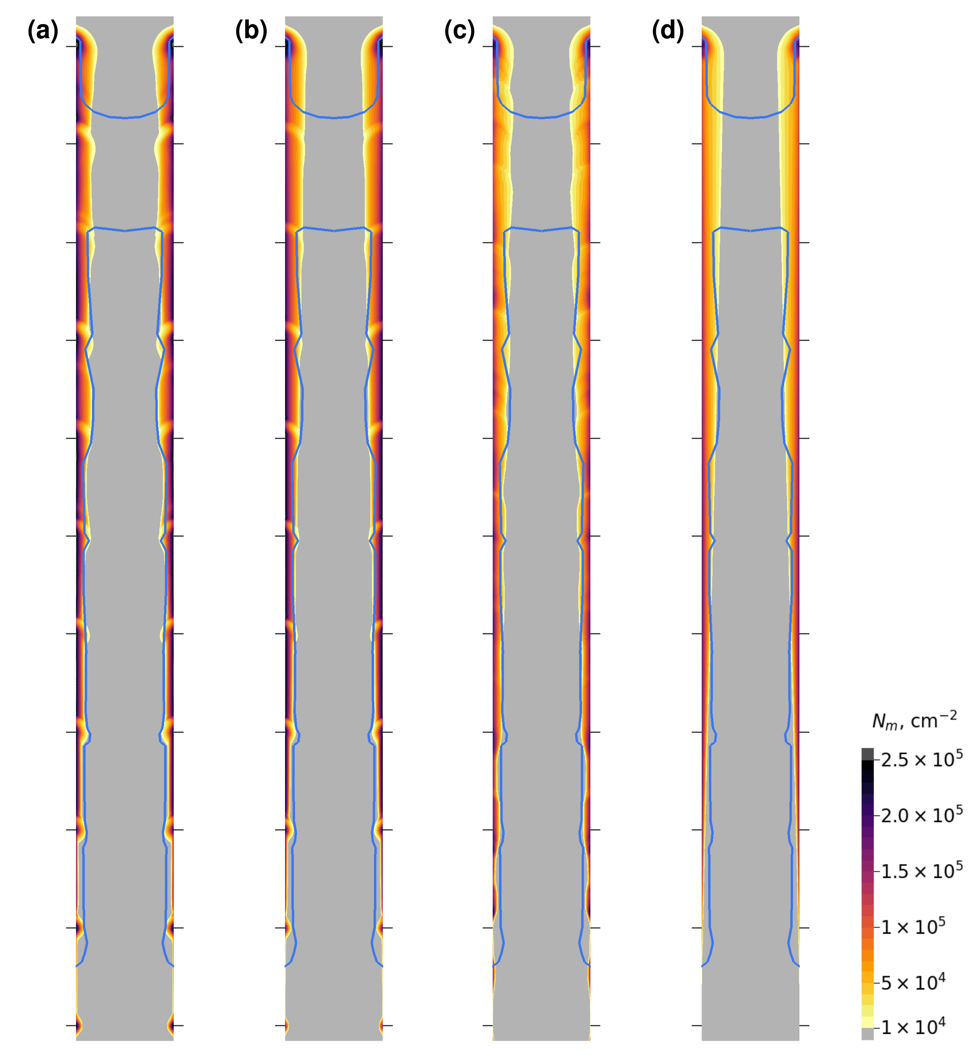
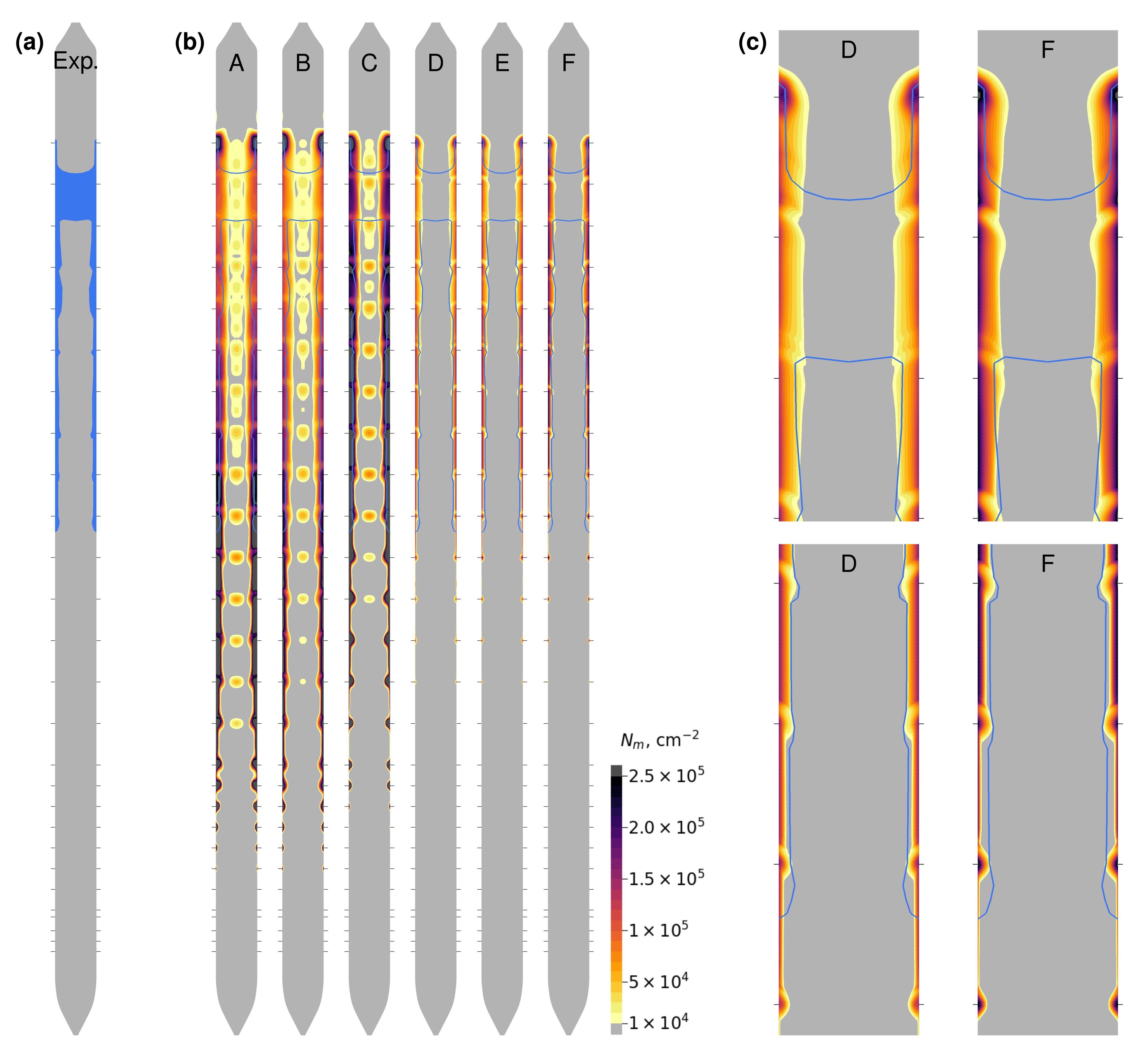
4.2. Dislocation Density Dynamics

Based on the validated heat transfer model (Section 4.1), the dislocation density simulations were then carried out. Since the AH model parameters for Si are rather similar among different authors [9,11,12,14], the parameter set from [14] was used in the present work: b = 3.8 Å , D = 4.3 N / m , p = 1.1 , l = 1.0 , k 0 = 8.6 × 10 4 m 3.2 / N 1.1 / s , K = 3.1 × 10 4 m / N , Q = 2.17 e V , and τ crit = 0 , which is further referred to as the “basic” parameter set. The Poisson’s ratio, the Young’s modulus, and the thermal expansion coefficient are the same as in Section 4.1.
The initial dislocation density N 0 has to be specified. While it is believed that in the experiment the crystal is initially dislocation-free [18], a zero value cannot be used since no dislocation multiplication will occur according to the AH model. Taking into account that dislocation densities between 1 × 10 4 c m −2 and 2 × 10 5 c m −2 were experimentally measured [18], the value of N 0 = 100   c m 2 was selected. Although it is known that the influence of N 0 on the results is small for sufficiently low N 0 [12], an additional simulation with N 0 = 1   c m 2 was carried out.
From a numerical point of view, the same mesh and finite element order as for the temperature field was employed for the dislocation density simulations. In addition to the maximum time step of 0.6 s , a minimum step of 0.1 s was set to improve numerical accuracy during time intervals in which rapid dislocation multiplication occurs. The influence of the mesh size, the finite element order, and the time step for the dislocation density field was checked in a similar manner as for the temperature field and found out to be weak (below 4%), although some minor numerical effects were observed.
Table 1 gives an overview of the parameters for six dislocation density simulations A–F. The final results—calculated dislocation density distributions for all cases—are depicted in Figure 7, including the comparison with the experiment. The superimposed experimental data were extracted from the dislocation distribution shown in Figure 6 of ref. [18]. Note that (i) only qualitative measurements of the dislocation density distribution were done (without detailed microscopic mapping), thus the extracted dislocated zone shape might not be very accurate, and (ii) no clear dependence of the dislocation density and lifetime on the crystallographic direction on a crystal cross section was observed in the experiment [18]; therefore, the crystallographic plane is not indicated for the experimental data shown in Figure 7.
The critical stress was assumed equal to the CRSS from the literature [6]: τ crit ( T ) = 0.1 exp ( 10.55 + 10147 / T ) (in Pa ). It is applied in some cases, which, as explained further in the text, improves the agreement with the experiment. For reference, the values of τ crit at 700 ° C , 1000 ° C , and 1300 ° C were 129 M Pa , 11 M Pa , and 2.4 M Pa , respectively.
There is a number of tendencies that are common for all considered cases in the simulation: the dislocations first appear at the crystal surface due to the highest stresses. The effect of crystal stopping manifests itself not only at the surface but also near the crystal axis—the local N m increases, compared to a moving crystal situation. While the calculated dislocation density differs between cases, a typical value of 1 × 10 5 c m −2 agrees with the experimentally measured values. Finally, high dislocation densities are created after the inductor power has been turned off due to a rapid temperature drop, which causes high stresses.
The first two cases in Table 1—A and B—use the same AH model parameters but differ in the heat induction model. As visible in Figure 7, there are only slight differences in the results—the maximum value of the dislocation density near the crystal surface is higher for the LF case due to higher stresses. At higher positions, the central N m “blobs” increase in size until dislocations completely penetrate the crystal cross-section.
The agreement with the experiment for cases A and B was very poor—the dislocations appeared much earlier, and the sizes of the dislocated zones near the crystal surface and the crystal axis were too large. To improve the situation, the AH model parameters were adjusted; the LF heat induction mode was used in further cases since the differences, compared to the HF mode, were rather insignificant.
To lower the dislocation density and postpone the initial dislocation appearance, in case C, the activation energy was increased from 2.17 e V to 2.3 e V . The results are closer to the experiment, but not by a significant amount—there were still too many dislocations near the axis, and dislocations appeared too early, compared to the experiment. A further increase in Q would be impractical due to an unrealistically high N m (more than 4 e 5 c m -2) at the crystal surface and too-strong individual “bumps” at low heating positions.
Instead, a different approach was used for case D by setting the temperature-dependent critical stress τ crit . The initial dislocation appearance was much closer to the experimentally observed position; additionally, the boundary of the dislocated zone near the crystal surface matched the experiment, including local N m increases at crystal stopping points. On the other hand, two discrepancies were observed: (i) initial dislocations appeared too early, and their pattern was discontinuous; (ii) the central crystal region was always dislocation-free. The fact that no dislocations appeared near the axis is explained by a lower stress as well as a lower temperature, compared to the crystal surface (see Figure 5 and Figure 6) and a consequently higher critical stress.
The influence of the initial dislocation density was checked for case E by using a 100-times lower value, compared to case D. The results were almost the same, except for slightly higher (ca. by 10%) maximum N m values, which was hardly noticeable.
Finally, in case F, the critical stress was combined with the increased activation energy. The results were qualitatively unchanged, compared to case D; however, a somewhat undesirable increase in the dislocation density at the crystal surface known from case C was present.
While cases D–F showed the best overall agreement with the experiment, the AH model still failed to correctly predict the initial appearance of the dislocations, which was well-defined in the experiment. The reason is that as soon as the effective stress was larger than zero, the dislocation multiplication starts. Some too-early individual N m maxima at stopping points could be eliminated by increasing τ crit , but the qualitative behaviour will remain the same. Another disagreement is the lack of dislocations near the crystal axis at high positions (temperatures) due to considerably lower stresses, compared to the ones at the crystal surface. This could be a limitation of the AH model, which is only local and does not include propagation of dislocations.
As mentioned before, both the inductor current I ( t ) and the heating position z ( t ) were changed in a stepwise manner. To further analyse their impact on the dislocation distribution, additional simulations based on case F were carried out in which the stepwise curves were replaced by linear time functions. The results shown in Figure 8 indicate that the effect of z ( t ) was the strongest since almost the same results were obtained for the linear I ( t ) curve (Figure 8b). If only I ( t ) was changed stepwise (Figure 8c), a quite different, more homogeneous dislocation density distribution was obtained. Finally, when both quantities were varied linearly (Figure 8d), a very smooth dislocated zone shape was predicted with its extension from the crystal surface changing from zero approximately at the position observed in the experiment to the maximum value at the end of heating. Additional parameter studies with the developed model could be carried out in the future.

5. Summary and Conclusions

A new numerical model in open-source library deal.II was developed for the simulation of the temperature field and the dislocation density dynamics. It is freely available as a new open-source solver package MACPLAS [20].
A previously published FZ Si crystal heating experiment was modelled numerically with the new model. A very good agreement with experimental measurements was obtained for the transient temperature field generated by a high-frequency inductor. Local temperature and stress maxima were observed at positions in which the crystal is not moving. Very small differences between low-frequency and high-frequency heat induction models were observed for temperature and elastic stress fields.
The Alexander–Haasen model was applied for the dislocation density dynamics. The inclusion of a temperature-dependent critical stress with a typical value of 11 M Pa at 1000 ° C was shown to be adequate for a more accurate description of the experimental results. In particular, the correct extension of the dislocated zone from the crystal surface was predicted, and the local increase in dislocation density at stopping points was present both in simulations and the experiment. There were no significant differences between both heat induction models as well as between cases with stepwise and linear inductor current curves.
The initial dislocation appearance and the fully dislocated crystal cross-section at high temperatures were not reproduced well by the simulations. A more sophisticated model considering, e.g., the propagation of dislocations would probably be required to fully explain the experimentally observed dislocation distribution. However, it should also be noted that only a single growth and heating experiment has been analysed so far. Further experiments and simulations would be beneficial.

Author Contributions

Conceptualization, A.S., K.D., R.M. and J.V.; methodology, A.S. and K.D.; software, A.S.; validation, A.S.; formal analysis, A.S. and K.D.; investigation, A.S. and K.D.; writing—original draft preparation, A.S.; writing—review and editing, K.D., R.M. and J.V.; visualization, A.S.; supervision, J.V.; project administration, A.S.; funding acquisition, A.S. All authors have read and agreed to the published version of the manuscript.

Funding

A.S. acknowledges financial support from the PostDoc Latvia Project No. 1.1.1.2/VIAA/2/18/280.

Data Availability Statement

The data presented in this study are available within the article.

Acknowledgments

The authors thank H.-J. Rost and F. M. Kießling for useful discussions. A.S. thanks K. Surovovs for technical assistance with extracting the temperature distribution from infrared images.

Conflicts of Interest

The authors declare no conflict of interest.

Abbreviations

The following abbreviations are used in this manuscript:
AHAlexander–Haasen
CRSSCritical resolved shear stress
CZCzochralski
EMElectromagnetic
FZFloating-zone
HFHigh-frequency
LFLow-frequency

Appendix A. Derivation of 1D Temperature Distribution for HF and LF Heat Induction Models

Let L δ be the domain size and 0 x L the coordinate in 1D. x = 0 corresponds to the crystal surface.
The steady-state temperature equation is solved assuming homogeneous material properties. The equation for the HF case is d 2 T / d x 2 = 0 , with the solution
T HF ( x ) = T 0 G x ,
where T 0 is the temperature at x = 0 , and G > 0 is the magnitude of the temperature gradient.
In the LF case, the volumetric heat heat source q ˙ = 2 q HF exp ( 2 x / δ ) / δ is included in the temperature equation: d 2 T / d x 2 = q ˙ / λ . The solution at large x should correspond to the HF case; therefore, the following boundary conditions at x = L were applied: T ( L ) = T 0 G L and d T / d x ( L ) = G . The first integration leads to
T x = q HF λ exp ( 2 x δ ) + c 1 ,
where the constant c 1 = G was determined from the second boundary condition and the fact that exp ( 2 L / δ ) 0 . The second integration gives
T = δ q HF 2 λ exp ( 2 x δ ) G x + c 2 ,
where the constant c 2 = T 0 was determined from the first boundary condition. The final result is
T LF ( x ) = T 0 G x δ q HF 2 λ exp ( 2 x δ ) ,
which tends to the HF solution as δ approaches zero. The difference between the HF and LF solutions is
Δ T ( x ) = T HF ( x ) T LF ( x ) = δ q HF 2 λ exp ( 2 x δ ) .
According to Equation (3), the necessary EM power to maintain the temperature distribution (A1) is given by
q HF σ SB ε T 0 4 + λ G ,
where the ambient temperature and convective cooling are neglected as they are rather weak.

References

  1. Dash, W.C. Growth of silicon crystals free from dislocations. J. Appl. Phys. 1959, 30, 459–474. [Google Scholar] [CrossRef]
  2. Rost, H.J.; Menzel, R.; Siche, D.; Juda, U.; Kayser, S.; Kießling, F.M.; Sylla, L.; Richter, T. Defect formation in Si-crystals grown on large diameter bulk seeds by a modified FZ-method. J. Cryst. Growth 2018, 500, 5–10. [Google Scholar] [CrossRef]
  3. Menzel, R.; Rost, H.J.; Kießling, F.M.; Sylla, L. Float-zone growth of silicon crystals using large-area seeding. J. Cryst. Growth 2019, 515, 32–36. [Google Scholar] [CrossRef]
  4. Stoddard, N.; Russell, J.; Hixson, E.C.; She, H.; Krause, A.; Wolny, F.; Bertoni, M.; Naerland, T.U.; Sylla, L.; von Ammon, W. NeoGrowth silicon: A new high purity, low-oxygen crystal growth technique for photovoltaic substrates. Prog. Photovoltaics Res. Appl. 2018, 26, 324–331. [Google Scholar] [CrossRef]
  5. Jordan, A.S.; Caruso, R.; VonNeida, A.R.; Nielsen, J.W. A comparative study of thermal stress induced dislocation generation in pulled GaAs, InP, and Si crystals. J. Appl. Phys. 1981, 52, 3331–3336. [Google Scholar] [CrossRef]
  6. Miyazaki, N.; Uchida, H.; Munakata, T.; Fujioka, K.; Sugino, Y. Thermal stress analysis of silicon bulk single crystal during Czochralski growth. J. Cryst. Growth 1992, 125, 102–111. [Google Scholar] [CrossRef]
  7. Muižnieks, A.; Raming, G.; Mühlbauer, A.; Virbulis, J.; Hanna, B.; Ammon, W. Stress-induced dislocation generation in large FZ- and CZ-silicon single crystals—Numerical model and qualitative considerations. J. Cryst. Growth 2001, 230, 305–313. [Google Scholar] [CrossRef]
  8. Alexander, H.; Haasen, P. Dislocations and plastic flow in the diamond structure. In Solid State Physics; Seitz, F., Turnbull, D., Ehrenreich, H., Eds.; Elsevier: Amsterdam, The Netherlands, 1969; Volume 22, pp. 27–158. [Google Scholar] [CrossRef]
  9. Dillon, O.W.; Tsai, C.T.; de Angelis, R.J. Dislocation dynamics during the growth of silicon ribbon. J. Appl. Phys. 1986, 60, 1784–1792. [Google Scholar] [CrossRef]
  10. Völkl, J.; Müller, G. A new model for the calculation of dislocation formation in semiconductor melt growth by taking into account the dynamics of plastic deformation. J. Cryst. Growth 1989, 97, 136–145. [Google Scholar] [CrossRef]
  11. Tsai, C.T.; Dillon, O.W.; de Angelis, R.J. The constitutive equation for silicon and its use in crystal growth modeling. J. Eng. Mater. Technol. 1990, 112, 183–187. [Google Scholar] [CrossRef]
  12. Miyazaki, N.; Okuyama, S. Development of finite element computer program for dislocation density analysis of bulk semiconductor single crystals during Czochralski growth. J. Cryst. Growth 1998, 183, 81–88. [Google Scholar] [CrossRef]
  13. Dadzis, K.; Behnken, H.; Bähr, T.; Oriwol, D.; Sylla, L.; Richter, T. Numerical simulation of stresses and dislocations in quasi-mono silicon. J. Cryst. Growth 2016, 450, 14–21. [Google Scholar] [CrossRef]
  14. Gallien, B.; Albaric, M.; Duffar, T.; Kakimoto, K.; M’Hamdi, M. Study on the usage of a commercial software (Comsol-Multiphysics®) for dislocation multiplication model. J. Cryst. Growth 2017, 457, 60–64. [Google Scholar] [CrossRef]
  15. Yonenaga, I.; Sumino, K. Dislocation dynamics in the plastic deformation of silicon crystals I. Experiments. Phys. Status Solidi A 1978, 50, 685–693. [Google Scholar] [CrossRef]
  16. Suezawa, M.; Sumino, K.; Yonenaga, I. Dislocation dynamics in the plastic deformation of silicon crystals. II. Theoretical analysis of experimental results. Phys. Status Solidi A 1979, 51, 217–226. [Google Scholar] [CrossRef]
  17. Gao, B.; Jiptner, K.; Nakano, S.; Harada, H.; Miyamura, Y.; Sekiguchi, T.; Kakimoto, K. Applicability of the three-dimensional Alexander-Haasen model for the analysis of dislocation distributions in single-crystal silicon. J. Cryst. Growth 2015, 411, 49–55. [Google Scholar] [CrossRef]
  18. Rost, H.J.; Buchovska, I.; Dadzis, K.; Juda, U.; Renner, M.; Menzel, R. Thermally stimulated dislocation generation in silicon crystals grown by the Float-Zone method. J. Cryst. Growth 2020, 552, 125842. [Google Scholar] [CrossRef]
  19. Arndt, D.; Bangerth, W.; Davydov, D.; Heister, T.; Heltai, L.; Kronbichler, M.; Maier, M.; Pelteret, J.P.; Turcksin, B.; Wells, D. The deal.II library, version 8.5. J. Numer. Math. 2017, 25, 137–145. [Google Scholar] [CrossRef]
  20. MACPLAS: MAcroscopic Crystal PLAsticity Simulator. Available online: https://github.com/aSabanskis/MACPLAS (accessed on 16 November 2021).
  21. Ratnieks, G. Modelling of the Floating Zone Growth of Silicon Single Crystals with Diameter up to 8 Inch. Ph.D. Thesis, University of Latvia, Riga, Latvia, 2007. [Google Scholar]
  22. Muhlbauer, A.; Muiznieks, A.; Leßmann, H.J. The calculation of 3D high-frequency electromagnetic fields during induction heating using the BEM. IEEE Trans. Magn. 1993, 29, 1566–1569. [Google Scholar] [CrossRef]
  23. Fulkerson, W.; Moore, J.P.; Williams, R.K.; Graves, R.S.; McElroy, D.L. Thermal conductivity, electrical resistivity, and Seebeck coefficient of silicon from 100 to 1300°K. Phys. Rev. 1968, 167, 765–782. [Google Scholar] [CrossRef]
  24. Sabanskis, A.; Plāte, M.; Sattler, A.; Miller, A.; Virbulis, J. Evaluation of the performance of published point defect parameter sets in cone and body phase of a 300 mm Czochralski silicon crystal. Crystals 2021, 11, 460. [Google Scholar] [CrossRef]
  25. Sabanskis, A.; Virbulis, J. Simulation of the influence of gas flow on melt convection and phase boundaries in FZ silicon single crystal growth. J. Cryst. Growth 2015, 417, 51–57. [Google Scholar] [CrossRef]
  26. Geuzaine, C.; Remacle, J.F. Gmsh: A 3-D finite element mesh generator with built-in pre- and post-processing facilities. Int. J. Numer. Methods Eng. 2009, 79, 1309–1331. [Google Scholar] [CrossRef]
  27. Okada, Y.; Tokumaru, Y. Precise determination of lattice parameter and thermal expansion coefficient of silicon between 300 and 1500 K. J. Appl. Phys. 1984, 56, 314–320. [Google Scholar] [CrossRef]
Figure 1. Infrared image 3 min before the end of heating. The superimposed horizontal white line shows the vertical position of the inductor mid-plane, while the vertical one denotes the location for the vertical temperature distribution T ( z ) . The main temperature reading of 1180.0 ° C is for a circular region ( 5.7 m m in diameter) below the inductor.
Crystals 12 00174 g001
Figure 2. Time dependence of experimental parameters—measured crystal temperature (average over the circular region in Figure 1), heating (crystal) position, and HF inductor power. Highlighted areas show time intervals at which the crystal is stationary.
Crystals 12 00174 g002
Figure 3. Comparison of time-dependent temperature with experimental measurements. T ( t ) for the HF simulation is not depicted as it practically overlaps with the LF result. Also shown is the maximum crystal temperature T max and inductor current I. Highlighted areas show time intervals at which the crystal is stationary.
Crystals 12 00174 g003
Figure 4. Comparison of vertical temperature distribution at different times with experimental measurements. Black vertical lines show the lower and the upper boundary of the measurement region. T ( z z 0 ) distribution at t = 125 min was symmetric with respect to the inductor, which allowed to obtain more precise measurement point coordinates.
Crystals 12 00174 g004
Figure 5. Comparison of radial distributions of temperature T and stress J 2 at the end of heating ( t = 215 min ) for LF and HF modes.
Crystals 12 00174 g005
Figure 6. Simulation results at the end of heating ( t = 215 min ); zoom-in at the upper part of the crystal. (a) temperature, (b) maximum temperature during the whole simulation, (c) elastic thermal stress. Left side: HF mode; right side: LF mode. Black horizontal lines in (b) show heating positions at which the crystal is not moving.
Crystals 12 00174 g006
Figure 7. (a) Shape of dislocated zone in experiment; (b) calculated dislocation density in the whole crystal according to cases A–F in Table 1; (c) zoomed-in simulation results at two positions for cases D and F. Experimentally observed boundary of the dislocated zone is depicted in (b,c) as blue curves. Black horizontal lines show heating positions at which the crystal is not moving.
Crystals 12 00174 g007
Figure 8. Dislocation density for simulation case F with varied I ( t ) and z ( t ) curves. (a) Default (stepwise) curves; (b) linear I ( t ) curve; (c) linear z ( t ) curve; (d) linear I ( t ) and z ( t ) curves. Experimentally observed boundary of the dislocated zone is depicted as blue curves. Black horizontal lines show heating positions at which the crystal was not moving.
Crystals 12 00174 g008
Table 1. Summary of considered cases.
CaseHeat Induction ModeDislocation Parameters
ALFBasic parameter set
BHFBasic parameter set
CLF Q = 2.3 e V
DLF τ crit ( T )
ELF τ crit ( T ) , N 0 = 1 c m 2
FLF τ crit ( T ) , Q = 2.3 e V
Publisher’s Note: MDPI stays neutral with regard to jurisdictional claims in published maps and institutional affiliations.

