
Preparation and Characterization of Cu and Al Doped ZnO Thin Films for Solar Cell Applications

 ,
,  ,
, 

Abstract
:1. Introduction
2. Materials and Methods
2.1. Materials
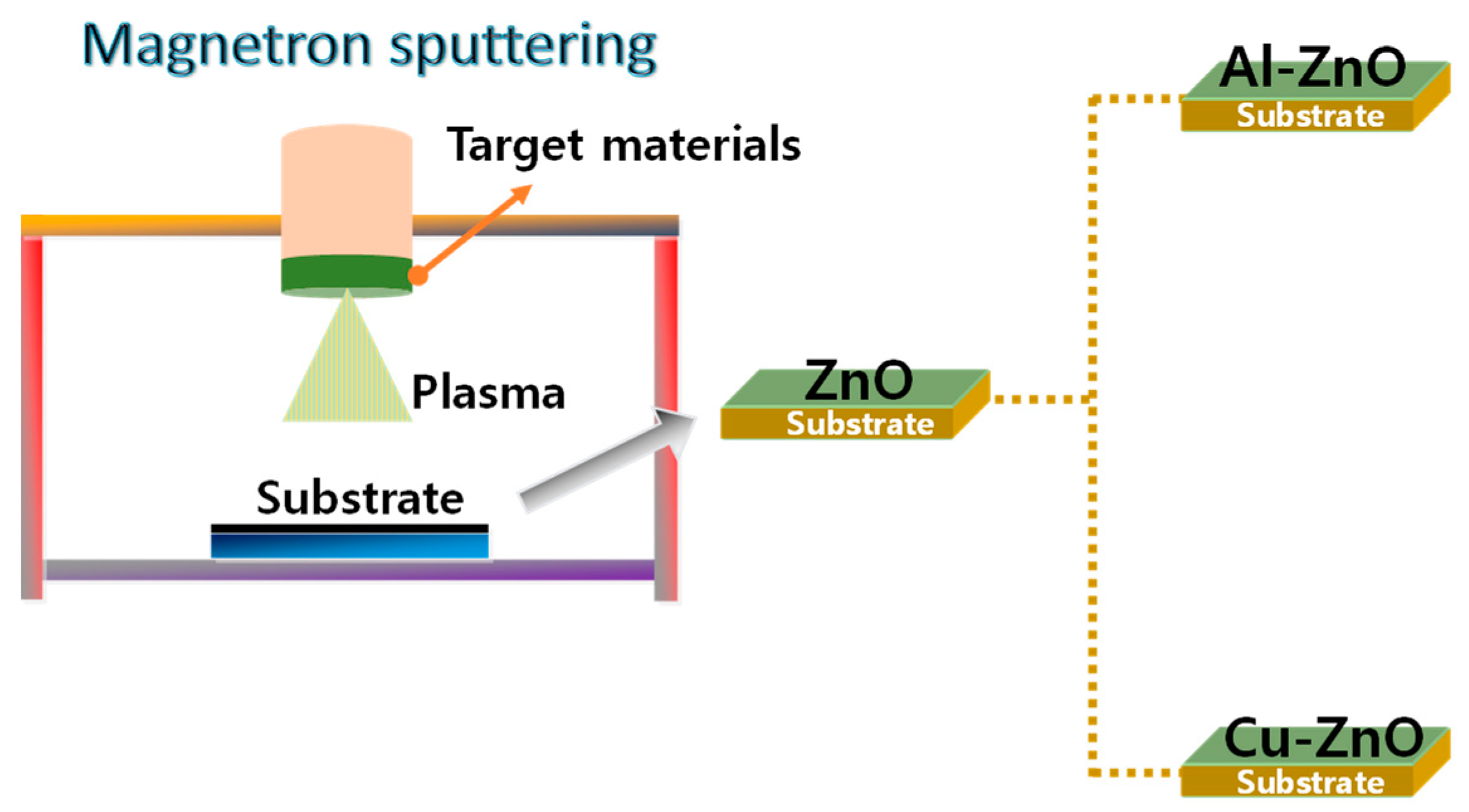
2.2. Methods
2.3. Solar Cell Fabrication and Characterization
2.4. Fabrication of the ZnO, Cu–ZnO, and Al–ZnO Film
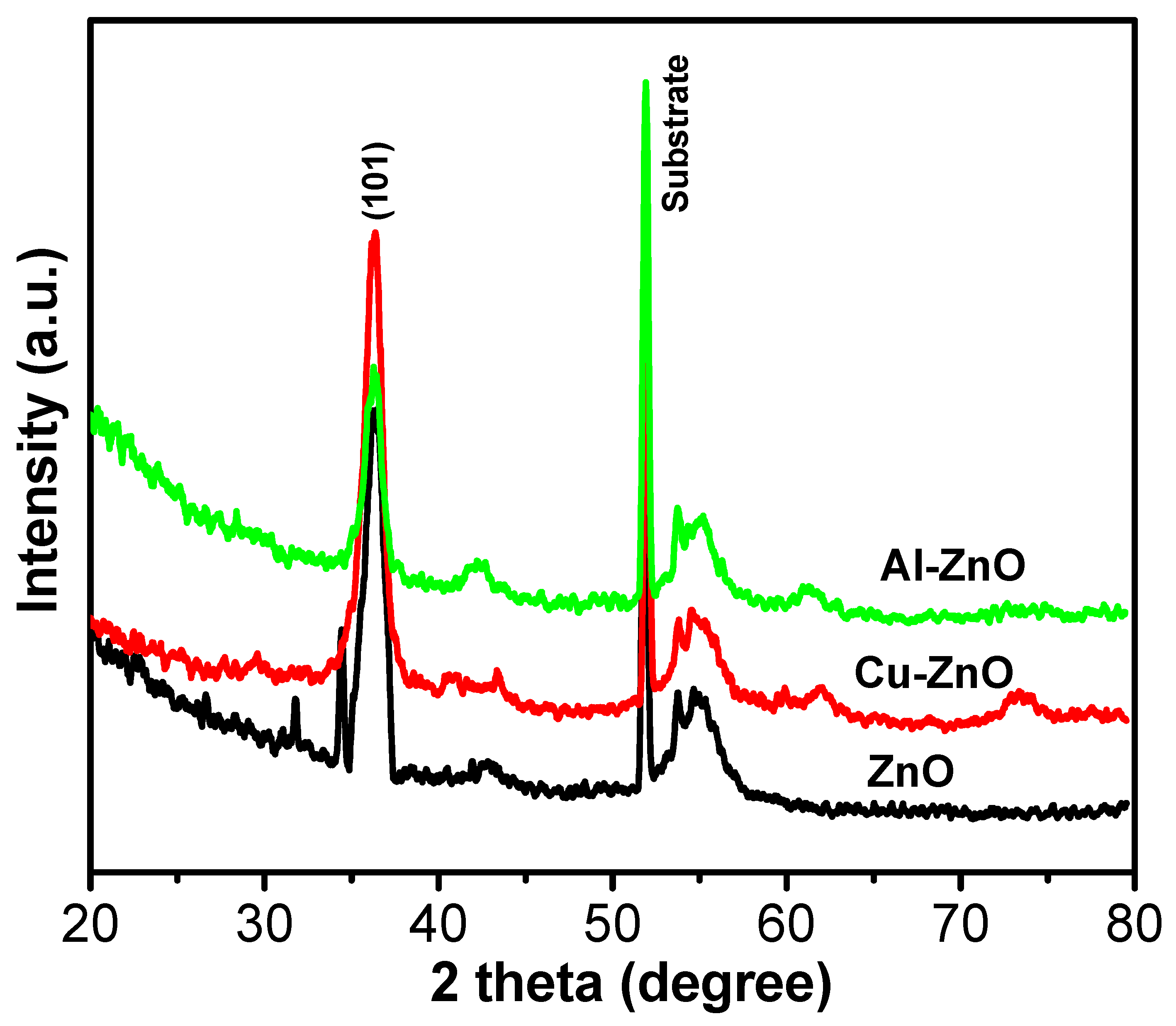
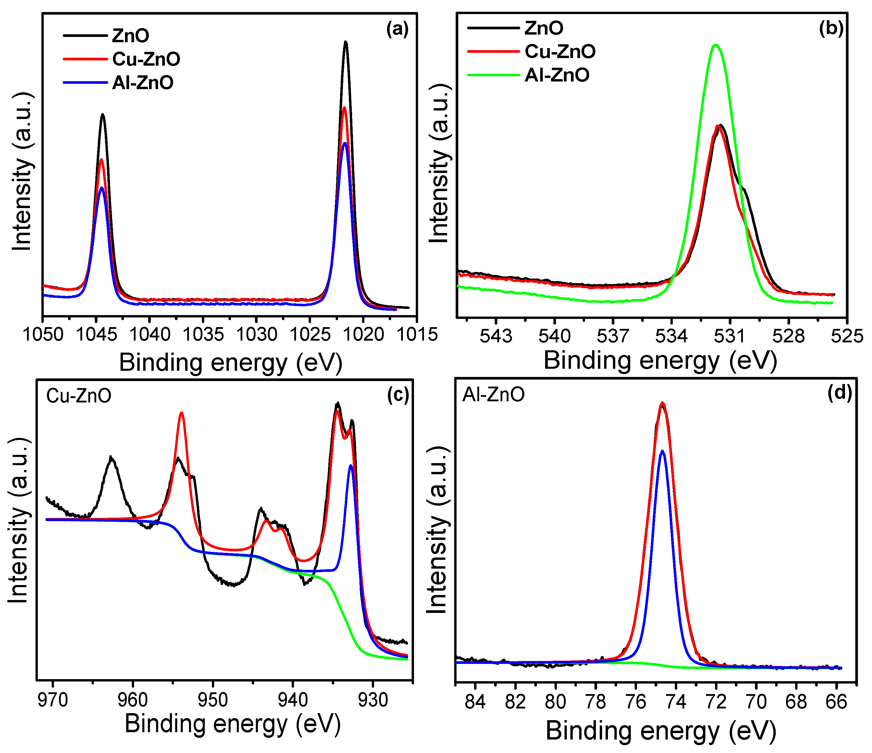
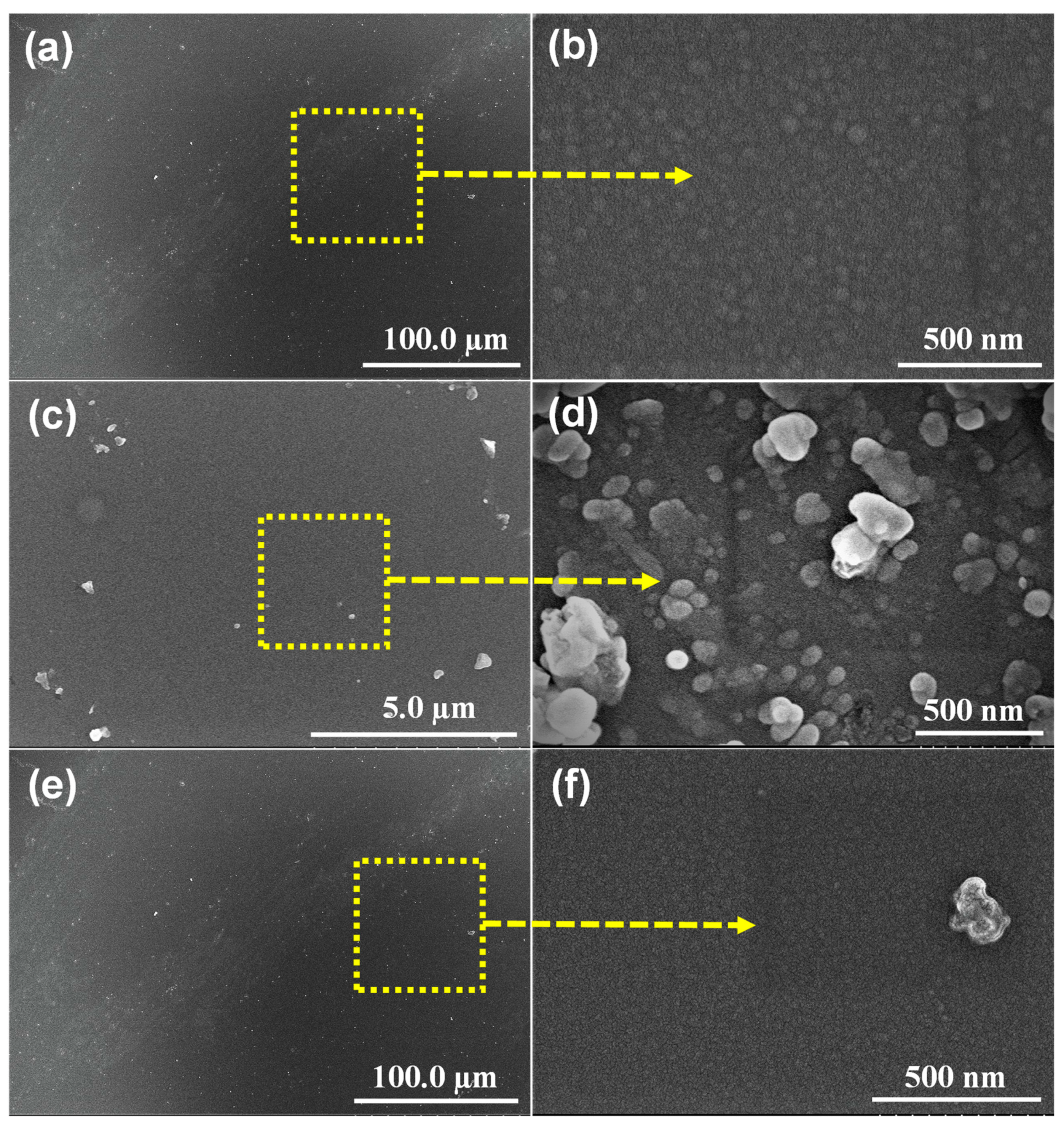
3. Results and Discussion
4. Conclusions
Author Contributions
Funding
Conflicts of Interest
References
- Ge, Z.; Wang, C.; Chen, T.; Chen, Z.; Wang, T.; Guo, L.; Qi, G.; Liu, J. Preparation of Cu-doped ZnO nanoparticles via layered double hydroxide and application for dye-sensitized solar cells. J. Phys. Chem. Solids 2021, 150, 109833. [Google Scholar] [CrossRef]
- Kharangarh, P.; Misra, D.; Georgiou, G.E.; Chin, K.K. Evaluation of Cu back contact related deep defects in CdTe solar cells. ECS J. Solid State Sci. Technol. 2012, 1, Q110. [Google Scholar] [CrossRef] [Green Version]
- Sufyan, M.; Mehmood, U.; Gill, Y.Q.; Nazar, R.; Khan, A.U.H. Hydrothermally synthesize zinc oxide (ZnO) nanorods as an effective photoanode material for third-generation Dye-sensitized solar cells (DSSCs). Mater. Lett. 2021, 297, 130017. [Google Scholar] [CrossRef]
- Ringleb, A.; Ruess, R.; Hofeditz, N.; Heimbrodt, W.; Yoshida, T.; Schlettwein, D. Influence of Mg-doping on the characteristics of ZnO photoanodes in dye-sensitized solar cells. Phys. Chem. Chem. Phys. 2021, 23, 8393–8402. [Google Scholar] [CrossRef]
- Quintana, M.; Edvinsson, T.; Hagfeldt, A.A.; Boschloo, G. Comparison of dye-sensitized ZnO and TiO2 solar cells: Studies of charge transport and carrier lifetime. J. Phys. Chem. C 2007, 11, 1035–1041. [Google Scholar] [CrossRef]
- Zhang, Q.; Xie, C.; Zhang, S.; Wang, A.; Zhu, B.; Wang, L.; Yang, Z. Identification and pattern recognition analysis of Chinese liquors by doped nano ZnO gas sensor array. Sens. Actuators B Chem. 2005, 110, 370–376. [Google Scholar] [CrossRef]
- Park, S.-M.; Ikegami, T.; Ebihara, K. Investigation of transparent conductive oxide Al-doped ZnO films produced by pulsed laser deposition. Jpn. J. Appl. Phys. 2005, 44, 8027. [Google Scholar] [CrossRef]
- Jongnavakit, P.; Amornpitoksuk, P.; Suwanboon, S.; Ndiege, N. Preparation and photocatalytic activity of Cu-doped ZnO thin films prepared by the sol–gel method. Appl. Surf. Sci. 2012, 258, 8192–8198. [Google Scholar] [CrossRef]
- Ke, Y.; Berry, J.; Parilla, P.; Zakutayev, A.; O’Hayre, R.; Ginley, D. The origin of electrical property deterioration with increasing Mg concentration in ZnMgO: Ga. Thin Solid Films 2012, 520, 3697–3702. [Google Scholar] [CrossRef]
- Purica, M.; Budianu, E.; Rusu, E.; Danila, M.A.; Gavrila, R. Optical and structural investigation of ZnO thin films prepared by chemical vapor deposition (CVD). Thin Solid Films 2002, 403, 485–488. [Google Scholar] [CrossRef]
- Sbrockey, N.M.; Ganesan, S. ZnO thin films by MOCVD. III-Vs Rev. 2004, 17, 23–25. [Google Scholar] [CrossRef] [Green Version]
- Park, T.; Kong, B.; Cho, H.K.; Park, D.; Lee, J. Influence of gas atmosphere during growth interruption in the deposition of ZnO films by magnetron sputtering. Phys. B Condens. Matter 2006, 376, 735–740. [Google Scholar] [CrossRef]
- Ghosh, A.; Kumari, N.; Bhattacharjee, A. Influence of Cu doping on the structural, electrical and optical properties of ZnO. Pramana 2015, 84, 621–635. [Google Scholar] [CrossRef]
- Yang, W.; Liu, Z.; Peng, D.-L.; Zhang, F.; Huang, H.; Xie, Y.; Wu, Z. Room-temperature deposition of transparent conducting Al-doped ZnO films by RF magnetron sputtering method. Appl. Surf. Sci. 2009, 255, 5669–5673. [Google Scholar] [CrossRef]
- Nomoto, J.-I.; Hirano, T.; Miyata, T.; Minami, T. Preparation of Al-doped ZnO transparent electrodes suitable for thin-film solar cell applications by various types of magnetron sputtering depositions. Thin Solid Films 2011, 520, 1400–1406. [Google Scholar] [CrossRef]
- Hirahara, N.; Onwona-Agyeman, B.; Nakao, M. Preparation of Al-doped ZnO thin films as transparent conductive substrate in dye-sensitized solar cell. Thin Solid Films 2012, 520, 2123–2127. [Google Scholar] [CrossRef]
- Sun, J.H.; Dong, S.Y.; Feng, J.L.; Yin, X.J.; Zhao, X.C. Enhanced sunlight photocatalytic performance of Sn-doped ZnO for Methylene Blue degradation. J. Mol. Catal. A Chem. 2011, 335, 145–150. [Google Scholar] [CrossRef]
- Saputrina, T.T.; Iwantono, I.; Awitdrus, A.; Umar, A.A. Performances of dye-sensitized solar cell (DSSC) with working electrode of aluminum-doped ZnO nanorods. Sci. Technol. Commun. J. 2020, 1, 1. [Google Scholar]
- Lee, J.H.; Song, J.T. Dependence of the electrical and optical properties on the bias voltage for ZnO: Al films deposited by rf magnetron sputtering. Thin Solid Films 2008, 516, 1377–1381. [Google Scholar] [CrossRef]
- Wang, H.; Xu, J.; Ren, M.; Yang, L. Room temperature deposition and properties of ZnO: Al thin films by nonreactive DC magnetron sputtering. J. Mater. Sci. Mater. Electron. 2008, 19, 1135–1139. [Google Scholar] [CrossRef]
- Lin, W.; Ma, R.; Shao, W.; Kang, B.; Wu, W. Properties of doped ZnO transparent conductive thin films deposited by RF magnetron sputtering using a series of high quality ceramic targets. Rare Met. 2008, 27, 32–35. [Google Scholar] [CrossRef]
- Iwantono, I.; Saad, S.K.M.; Anggelina, F.; Awitdrus, A.; Ramli, M.A.; Umar, A.A. Enhanced charge transfer activity in Au nanoparticles decorated ZnO nanorods photoanode. Phys. E Low-Dimens. Syst. Nanostruct. 2019, 111, 44–50. [Google Scholar] [CrossRef]
- Waqas Alam, M.; Khatoon, U.; Qurashi, A. Synthesis and characterization of Cu-SnO2 nanoparticles deposited on glass using ultrasonic spray pyrolysis and their H2S sensing properties. Curr. Nanosci. 2012, 8, 919–924. [Google Scholar] [CrossRef]
- Park, M.S.; Min, B.I. Ferromagnetism in ZnO codoped with transition metals: Zn1−x(FeCo)xO and Zn1−x(FeCu)xO. Phys. Rev. B 2003, 68, 224436. [Google Scholar] [CrossRef] [Green Version]
- Buchholz, D.B.; Chang, R.P.H.; Song, J.Y.; Ketterson, J.B. Room-temperature ferromagnetism in Cu-doped ZnO thin films. Appl. Phys. Lett. 2005, 87, 082504. [Google Scholar] [CrossRef]
- Mohan, R.; Krishnamoorthy, K.; Kim, S.J. Enhanced photocatalytic activity of Cu-doped ZnO nanorods. Solid State Commun. 2012, 152, 375–380. [Google Scholar] [CrossRef]
- Raja, M.; Muthukumarasamy, N.; Velauthapillai, D.; Balasundaraprabhu, R. Influence of copper on the morphology and properties of one dimensional ZnO nanorod structures. Superlattices Microstruct. 2014, 72, 102–110. [Google Scholar] [CrossRef]
- Aravind, A.; Jayaraj, M.K.; Kumar, M.; Chandra, R. Optical and magnetic properties of copper doped ZnO nanorods prepared by hydrothermal method. J. Mater. Sci. Mater. Electron. 2013, 24, 106–112. [Google Scholar] [CrossRef]
- Ma, Z.; Ren, F.; Ming, X.; Long, Y.; Volinsky, A.A. Cu-doped ZnO electronic structure and optical properties studied by first-principles calculations and experiments. Materials 2019, 12, 196. [Google Scholar] [CrossRef] [PubMed] [Green Version]
- Chen, M.; Pei, Z.; Sun, C.; Wen, L.; Wang, X. Surface characterization of transparent conductive oxide Al-doped ZnO films. J. Cryst. Growth 2000, 220, 254–262. [Google Scholar] [CrossRef]
- Asemi, M.; Ahmadi, M.; Ghanaatshoar, M. Preparation of highly conducting Al-doped ZnO target by vacuum heat-treatment for thin film solar cell applications. Ceram. Int. 2018, 44, 12862–12868. [Google Scholar] [CrossRef]
- Raja, M.; Muthukumarasamy, N.; Velauthapillai, D.; Balasundraprabhu, R.; Agilan, S.; Senthil, T.S. Quantum dot sensitized aluminium doped and copper doped ZnO nanostructure based solar cells. J. Mater. Sci. Mater. Electron. 2014, 25, 5035–5040. [Google Scholar] [CrossRef]
- Lee, D.J.; Kim, H.M.; Kwon, J.Y.; Choi, H.; Kim, S.H.; Kim, K.B. Structural and electrical properties of atomic layer deposited Al-doped ZnO films. Adv. Funct. Mater. 2011, 21, 448–455. [Google Scholar] [CrossRef]
- Lee, Y.M.; Lai, C.H. Preparation and characterization of solid n-TiO2/p-NiO hetrojunction electrodes for all-solid-state dye-sensitized solar cells. Solid-State Electron. 2009, 53, 1116–1125. [Google Scholar] [CrossRef]
- Das, A.; Wary, R.R.; Nair, R.G. Cu modified ZnO nanoflakes: An efficient visible light-driven photocatalyst and a promising photoanode for dye sensitized solar cell (DSSC). Solid State Sci. 2020, 104, 106290. [Google Scholar] [CrossRef]


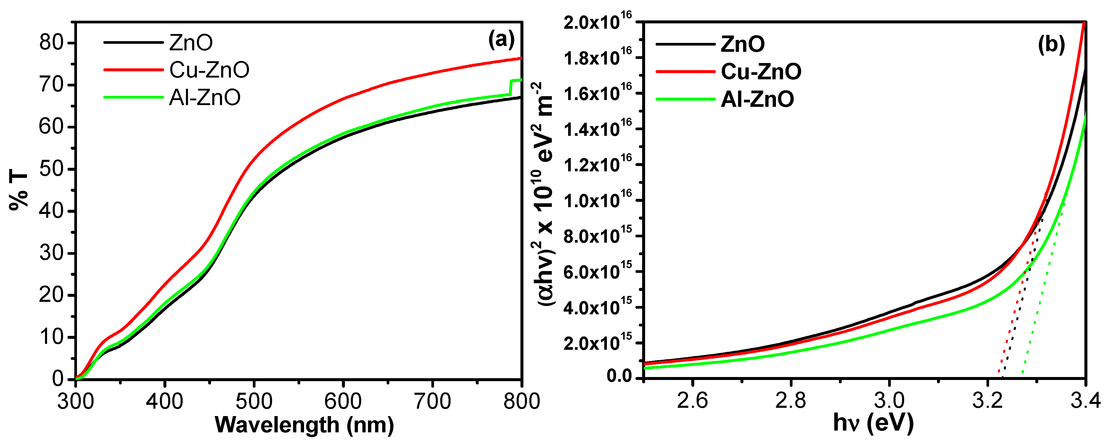
| Sample | Hall Mobility (cm2 V−1 S−1) | Carrier Concentration (cm−3) | Resistivity (Ω cm) | Conductivity (S cm−1) |
|---|---|---|---|---|
| ZnO | 11.3 | 2.7 × 10²⁰ | 4.1 × 10⁻⁴ | 2.4 × 10³ |
| Al–ZnO | 16.1 | 3.5 × 10²¹ | 3.2 × 10⁻⁴ | 3.4 × 10³ |
| Cu–ZnO | 13.2 | 4.3 × 10²¹ | 2.04 × 10⁻⁴ | 5.8 × 10³ |
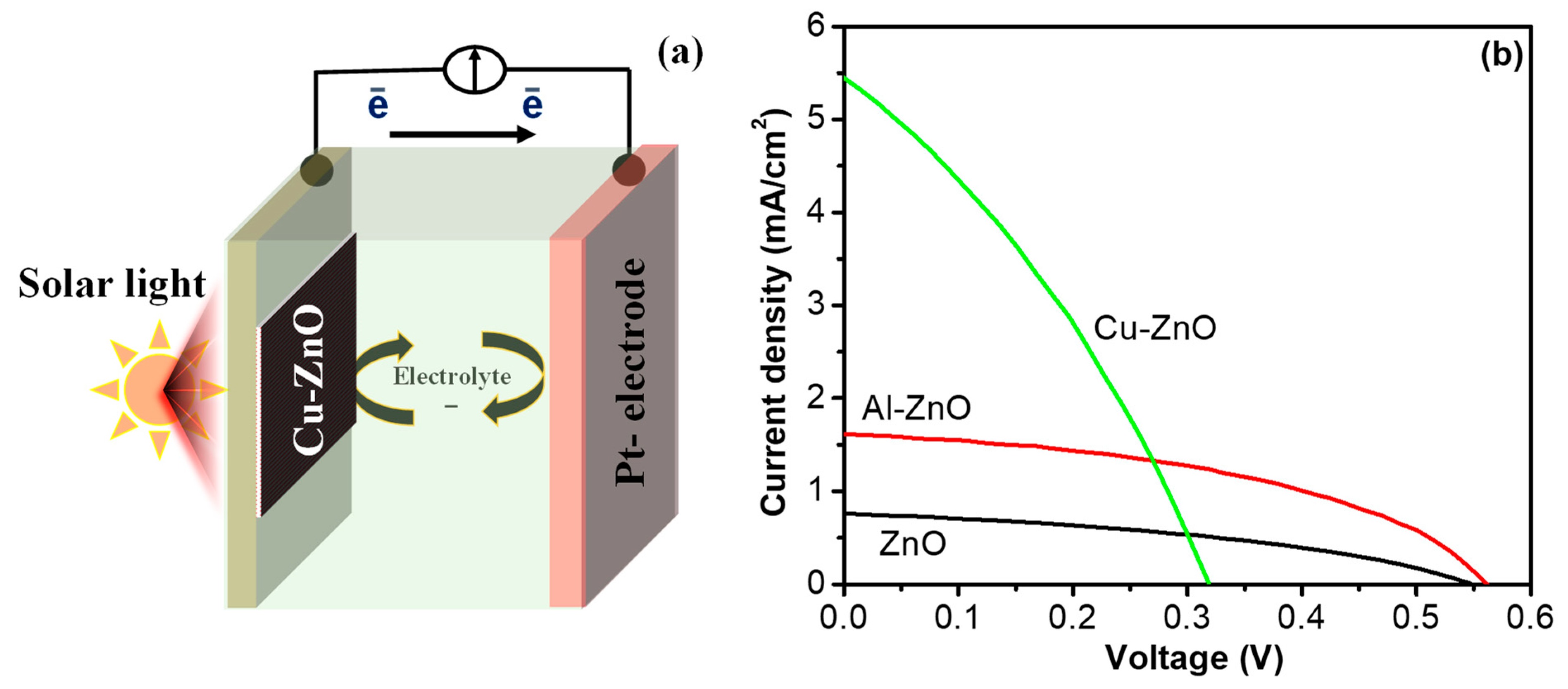
| Sample | Voc (V) | Jsc (mA/cm2) | PEC (%) |
|---|---|---|---|
| ZnO | 0.533 | 0.762 | 0.163 |
| Al–ZnO | 0.547 | 1.539 | 0.492 |
| Cu–ZnO | 0.315 | 4.985 | 0.559 |
Publisher’s Note: MDPI stays neutral with regard to jurisdictional claims in published maps and institutional affiliations. |
© 2022 by the authors. Licensee MDPI, Basel, Switzerland. This article is an open access article distributed under the terms and conditions of the Creative Commons Attribution (CC BY) license (https://creativecommons.org/licenses/by/4.0/).
Share and Cite
Alam, M.W.; Ansari, M.Z.; Aamir, M.; Waheed-Ur-Rehman, M.; Parveen, N.; Ansari, S.A. Preparation and Characterization of Cu and Al Doped ZnO Thin Films for Solar Cell Applications. Crystals 2022, 12, 128. https://doi.org/10.3390/cryst12020128
Alam MW, Ansari MZ, Aamir M, Waheed-Ur-Rehman M, Parveen N, Ansari SA. Preparation and Characterization of Cu and Al Doped ZnO Thin Films for Solar Cell Applications. Crystals. 2022; 12(2):128. https://doi.org/10.3390/cryst12020128
Chicago/Turabian StyleAlam, Mir Waqas, Mohd Zahid Ansari, Muhammad Aamir, Mir Waheed-Ur-Rehman, Nazish Parveen, and Sajid Ali Ansari. 2022. "Preparation and Characterization of Cu and Al Doped ZnO Thin Films for Solar Cell Applications" Crystals 12, no. 2: 128. https://doi.org/10.3390/cryst12020128
APA StyleAlam, M. W., Ansari, M. Z., Aamir, M., Waheed-Ur-Rehman, M., Parveen, N., & Ansari, S. A. (2022). Preparation and Characterization of Cu and Al Doped ZnO Thin Films for Solar Cell Applications. Crystals, 12(2), 128. https://doi.org/10.3390/cryst12020128