


Effect of Growth Temperature on Crystallization of Ge1−xSnx Films by Magnetron Sputtering
by
Hongjuan Huang
1,2,3,
Desheng Zhao
2,4,
Chengjian Qi
4,
Jingfa Huang
4,
Zhongming Zeng
2,
Baoshun Zhang
2,* and
Shulong Lu
1,3,* 1
School of Nano-Tech and Nano-Bionics, University of Science and Technology of China, Hefei 230026, China
2
Nano Fabrication Facility, Suzhou Institute of Nano-Tech and Nano-Bionics, Chinese Academy of Sciences (CAS), Suzhou 215123, China
3
Key Lab of Nanodevices and Applications, Suzhou Institute of Nano-Tech and Nano-Bionics, Chinese Academy of Sciences (CAS), Suzhou 215123, China
4
Nano Fabrication Facility, Guangdong Institute of Semiconductor Micro-Nano Manufacturing Technology, Guangdong 528200, China
*
Authors to whom correspondence should be addressed.
Crystals 2022, 12(12), 1810; https://doi.org/10.3390/cryst12121810
Submission received: 16 November 2022
/
Revised: 1 December 2022
/
Accepted: 8 December 2022
/
Published: 12 December 2022
(This article belongs to the Special Issue Novel Wide-Bandgap Semiconductor Materials and Devices)
Abstract
:Ge1−xSnx film with Sn content (at%) as high as 13% was grown on Si (100) substrate with Ge buffer layer by magnetron sputtering epitaxy. According to the analysis of HRXRD and Raman spectrum, the quality of the Ge1−xSnx crystal was strongly dependent on the growth temperature. Among them, the GeSn (400) diffraction peak of the Ge1−xSnx film grown at 240 °C was the lowest, which is consistent with the Raman result. According to the transmission electron microscope image, some dislocations appeared at the interface between the Ge buffer layer and the Si substrate due to the large lattice mismatch, but a highly ordered atomic arrangement was observed at the interface between the Ge buffer layer and the Ge1−xSnx layer. The Ge1−xSnx film prepared by magnetron sputtering is expected to be a cost-effective fabrication method for Si-based infrared devices.
1. Introduction
Ge1−xSnx alloys have attracted considerable attention in Si-based optoelectronic device integration because of their enhanced carrier mobility, adjustable band gap structure and compatibility with the CMOS processes [1,2,3,4,5]. Efficient devices based on Ge1−xSnx have been fabricated, including thin film transistors [6,7,8,9], solar cells [10], photodetectors [11,12,13], LEDs [14,15,16,17], lasers [18,19], etc. By adjusting the content of Sn and the strain of Ge1−xSnx, the direct band gap can be extended to mid-infrared applications [20,21,22]. However, there are some difficulties in preparing Ge1−xSnx alloys with high Sn content and good crystal quality on a Si substrate [23,24]. At first, the equilibrium solid solubility of Sn in Ge is as low as about 0.5% [25]. Secondly, the phenomenon of Sn segregation easily appears during fabrication. Thirdly, the lattice mismatch between Ge and α-Sn is about 14.7% [26]. Thus, determining how to achieve a high Sn content and good quality Ge1−xSnx alloy is critical for fabricating high-performance Ge1−xSnx photoelectronic devices.
So far, researchers have successfully prepared Ge1−xSnx alloy films using molecular beam epitaxy (MBE) [27,28,29], chemical vapor deposition (CVD) [30,31,32], magnetron sputtering [33,34,35,36] and solid phase crystallization [37,38]. Among these methods, MBE is a method that can accurately control the thickness and structure of thin films. However, once the layer thickness exceeds the critical thickness [39,40], the screw dislocation begins to appear, which is caused by lattice mismatch, thus affecting the crystal quality of the material. CVD can release misfit dislocations at the interface rather than forming through dislocations, so the thin film materials epitaxy by this technology have perfect crystal quality [41,42,43]. Magnetron sputtering is a low-cost and feasible method for Ge1−xSnx mass production. Qian, L. et al. used Ge (100) and GaAs (100) substrates with high lattice matching to obtain a Ge1−xSnx layer with good crystal quality by sputtering [44,45,46]. Grant, J. et al. adopted a CMOS compatible Si (100) substrate, and the Ge1−xSnx layer obtained by sputtering was polycrystalline [34,47,48]. There are few published papers about obtaining single crystal Ge1−xSnx on silicon substrate by sputtering. Zheng Jun et al. [24] realized Ge1−xSnx single crystal film with low Sn content on Ge/Si (100) substrate, in which Ge was the buffer layer, the deposition temperature was 400 °C, the deposition temperature of Ge1−xSnx films was 150 °C, and the highest Sn content was 0.06. Tsukamoto, T. et al. [49] deposited single crystal Ge1−xSnx film with x of about 0.115 on Si (100) substrate by magnetron sputtering without a buffer layer, and the deposition temperature was 250 °C. At present, single crystal Ge1−xSnx alloy films deposited on Si (100) substrate by epitaxial sputtering have the problems of many dislocations and low Sn doping, and the highest Sn doping is 0.115 [26,49,50]. Generally, when x is greater than 0.1, the energy band of Ge1−xSnx will be transformed into a direct band gap, so it is necessary to further increase the Sn content of single crystal Ge1−xSnx grown on silicon substrate by sputtering.
In this paper, we report the growth of Ge1−xSnx crystalline films on Si (100) substrates by sputtering. We have studied the possibility of growing single crystal Ge1−xSnx with Sn content more than 10% on Ge buffer layer. The Ge buffer layer was deposited at 300 °C, with a thickness of 572 nm. By adjusting the deposition temperature of Ge1−xSnx at 180~300 °C, single crystal Ge1−xSnx alloy films were obtained in which the highest Sn content (at%) reached 13%.
2. Materials and Methods
Ge1−xSnx epitaxial layers were deposited in a physical vapor deposition (PVD) system manufactured by ULVAC Corporation. Figure 1 is a schematic diagram of Ge1−xSnx deposition, in which Ge target and Sn target are installed at different target positions and sputtered at the same time. The substrate was placed on the bottom sample table, which can rotate horizontallyand move up and down and heat The sputtering rate of thin film was determined by sputtering power, sputtering distance, etc. The film thickness was obtained by scanning electron microscope profile test. Before deposition, we cleaned and activated the surface of the silicon substrate. Firstly, it was washed with sulfuric acid (H2SO4:H2O2 = 7:3) solution for 10 min and washed with deionized water 10 times to remove organic and inorganic pollution. Then, it was soaked in diluted HF (HF:H2O = 1:10) solution at room temperature for 30 s to remove the oxide layer on the surface. Finally, it was washed with deionized water 10 times and dried with nitrogen. The base pressure of the sputtering chamber was less than 4.0 × 10⁻⁴ Pa. Then, the substrate was quickly loaded into the growth chamber. After the vacuum degree reached 4.0 × 10⁻⁴ Pa, the substrate was heated at 300 °C for 1 h, and then the Ge buffer layer was deposited with a thickness of about 572 nm. Then, different Ge1−xSnx alloy films were deposited on the Ge buffer layer by changing the temperature of the substrate to 180 °C, 200 °C, 225 °C, 240 °C, 250 °C, 260 °C, 275 °C and 300 °C, respectively. The Ge1−xSnx film was deposited by Ge and Sn co-sputtering, and its thickness was about 350 nm. In the process of sputtering deposition, argon was filled to make the chamber pressure reach 0.4 Pa. The composition of the Ge1−xSnx films was achieved by maintaining a constant DC power of 130 W for the Ge target, and RF power of 40 W for the Sn target. The deposition rate of Ge and Sn were controlled about 1.2 Å/s, 0.22 Å/s, respectively. For comparison, the sample with only a Ge buffer layer was deposited under the same conditions as the samples with Ge1−xSnx alloy film.
The properties of the Ge buffer layer and the GeSn thin film were tested and analyzed by high-resolution X-ray diffraction (HR-XRD, X’pert PRO, PANalytical, Suzhou, China), Raman scattering (Raman, Labram HR 800,HORIBA Jobin Yvon, Suzhou, China), atomic force microscope (AFM, Dimension ICON, Bruker, Suzhou, China) and high-resolution transmission electron microscope (HRTEM, Talos F200X, Thermo Fisher Scientific, Suzhou, China). Among them, HR-XRD measured the 2 θ-ω diffraction peaks of (004) and (224) planes, with a step size of 0.05°, a time per size of 1s, and a scanning range of 60–72° and 78–92°, respectively. It was used to study the crystallization quality of single crystal films and calculate the Sn content according to the diffraction peak position and other information. A Raman scattering experiment was carried out at room temperature, the spectral line was 532 nm, exposure time was 5 s, the accumulation numbers were twice, and the scanning range was 200–350 cm−1. It was used to characterize the crystal quality and Sn composition of Ge1−xSnx film on the surface. AFM was used to characterize the surface roughness and morphology of Ge1−xSnx thin films in tapping mode with a scanning range of 5 μm × 5 μm, and to analyze the crystal particle size and morphology of the films. The working voltage of HRTEM is 200 kV. By observing the (110) surface of the sample, the atomic-scale material properties such as the lattice matching between materials, the crystal quality of single-layer materials and the composition ratio of alloy films could be analyzed.
Table 1 shows the parameters of the Ge1−xSnx samples, such as out-of-plane () lattice constants, in-plane () lattice constants, unstrained lattice constants (), measured Sn content (xm), degree of strain relaxation (R) and in-plane strain (). These parameters were calculated according to the HRXRD test results. According to Bragg’s law, the out-of-plane and in-plane lattice constants of the Ge1−xSnx layers were extracted from the positions of the peaks of GeSn (004) and GeSn (224), which are given by:
Then, the Sn composition of Ge1−xSnx layers could be calculated by simultaneously solving the Vegard’s law and the Poisson’s relationship, in which the bowing parameter of 0.004 nm in the Vegard’s law was considered [51], and the elastic constants of Ge1−xSnx layers in Poisson’s relationship was obtained by the linear interpolation of Ge and Sn. The R and were calculated according to the following equation:
where and are the lattice constants of the Ge Buffer and unstrained Ge1−xSnx layer, respectively.
As can be seen from Table 1, the content of Sn in the Ge1−xSnx film deposited at 240 °C is the highest, with the calculated value of 15.38%, which is 0.02 larger than the EDX test result of 13%, and the strain relaxation degree is also the highest, with the value of 93.2. The in-plane strain results show that all Ge1−xSnx films have small compressive stress, and the strain of Ge1−xSnx deposited at 240 °C is the largest. The results show that the unstrained lattice constant and stress increase with the increase of Sn content.
The Ge–Ge LO Raman peak () of Ge1−xSnx can be influenced by the Sn composition (x) and in-plane strain () as:
where is the bulk Ge Raman frequency at 301 cm−1, and the coefficients and are chosen as −95.1 and −435.6 cm−1, respectively [52,53]. According to the EDX test, the Sn content of the sample grown at 240 °C is about 13%, and the calculated Ge–Ge is 288.2 cm−1, which is close to the Raman measurement value of 287.5 cm−1.
3. Results and Discussion
Figure 2 shows the X-ray diffractograms of the Ge1−xSnx films deposited on buffered Ge layers in different conditions. The (004) and (224) plane XRD diffraction peaks of Si, Ge and GeSn are obvious in Figure 2. When the deposition temperature is between 180–250 °C, there is a diffraction peak of GeSn. This shows that the Ge1−xSnx alloy films under these process conditions are single crystal films. With the increase of deposition temperature, the diffraction peak intensity of Ge1−xSnx increases, and the position of diffraction peak decreases. At 240 °C, the intensity of the diffraction peak is the highest, and the position of the diffraction peak is the lowest, which indicates that the preferred orientation of Ge1−xSnx thin film crystal grown under this condition is obvious, and the Sn content is the highest. When the temperature rises to 260–300 °C, the diffraction peak of Ge widens, which indicates that the diffraction peak position of Ge1−xSnx is close to Ge; that is, the content of Sn drops sharply.
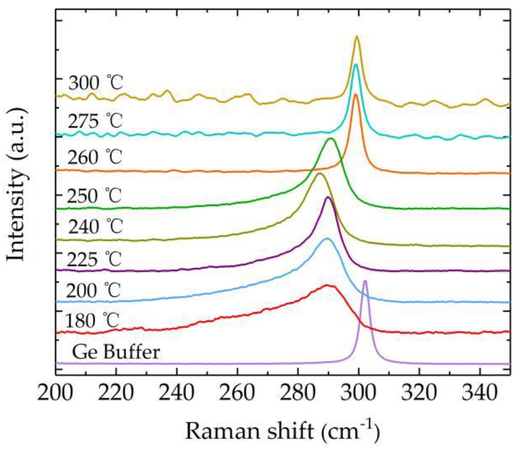
As we all know, Raman measurement is a common surface detection technology. By analyzing the intensity, peak position change and full width at half maximum of the Raman peak, the information of material composition, strain and crystal quality of semiconductor materials can be determined. Figure 3 shows the Raman spectrum of the Ge buffer layer and the Ge1−xSnx thin films prepared at different deposition temperatures. The spectrum of the Ge buffer can be seen to consist of one strong Ge–Ge LO Raman peak at 301.87 cm−1. Similarly, the spectra of the Ge1−xSnx films consists of a strong Ge–Ge LO Raman peak between 287.5 cm−1 and 290.6 cm−1. However, with the decrease of the deposition temperature of Ge1−xSnx, the Ge–Ge LO Raman peak in Ge1−xSnx alloys gradually widens and moves to a higher wavenumber. The Ge–Ge LO Raman peak of the thin film deposited at 240 °C is the lowest, which is in consistent with the results of HRXRD.
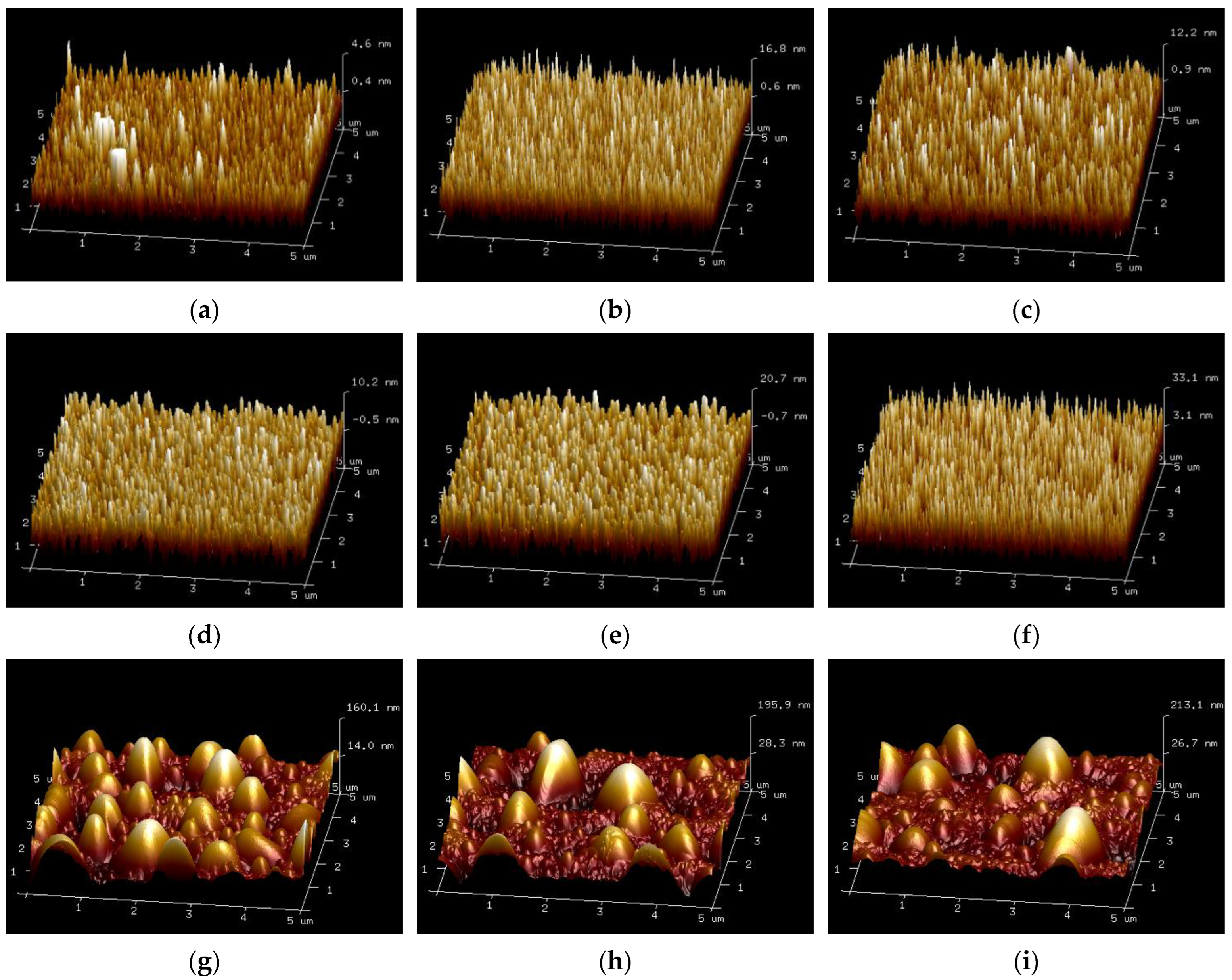
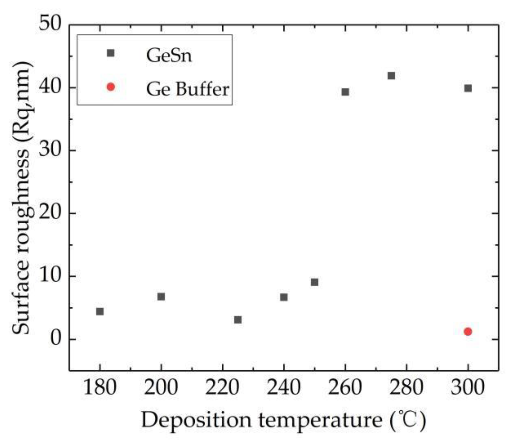
In order to determine the surface morphology of the Ge1−xSnx layer, atomic force microscopy (AFM) measurement was performed. Figure 4a–i shows the typical 5 µm × 5 µm AFM images of the Ge Buffer layer and Ge1−xSnx layers, and the RMS (root mean square roughness) value of the Ge1−xSnx samples was extracted from AFM scans. It was found that the root mean square roughness (Rq) value of Ge Buffer was 1.21 nm and that of Ge1−xSnx samples was 4.42–41.9 nm, respectively. Figure 5 shows the comparison results of Rq values of Ge and Ge1−xSnx samples. With the increase of temperature, the roughness increases at first, decreases at 200 °C and then increases continuously. When the temperature is higher than 260 °C, the roughness increases by an order of magnitude, and the surface of the sample is silvery white and evenly distributed. It can be explained that the increase of deposition temperature intensifies the segregation of Sn; the diameter of meta-Sn particles is about 2 μm.
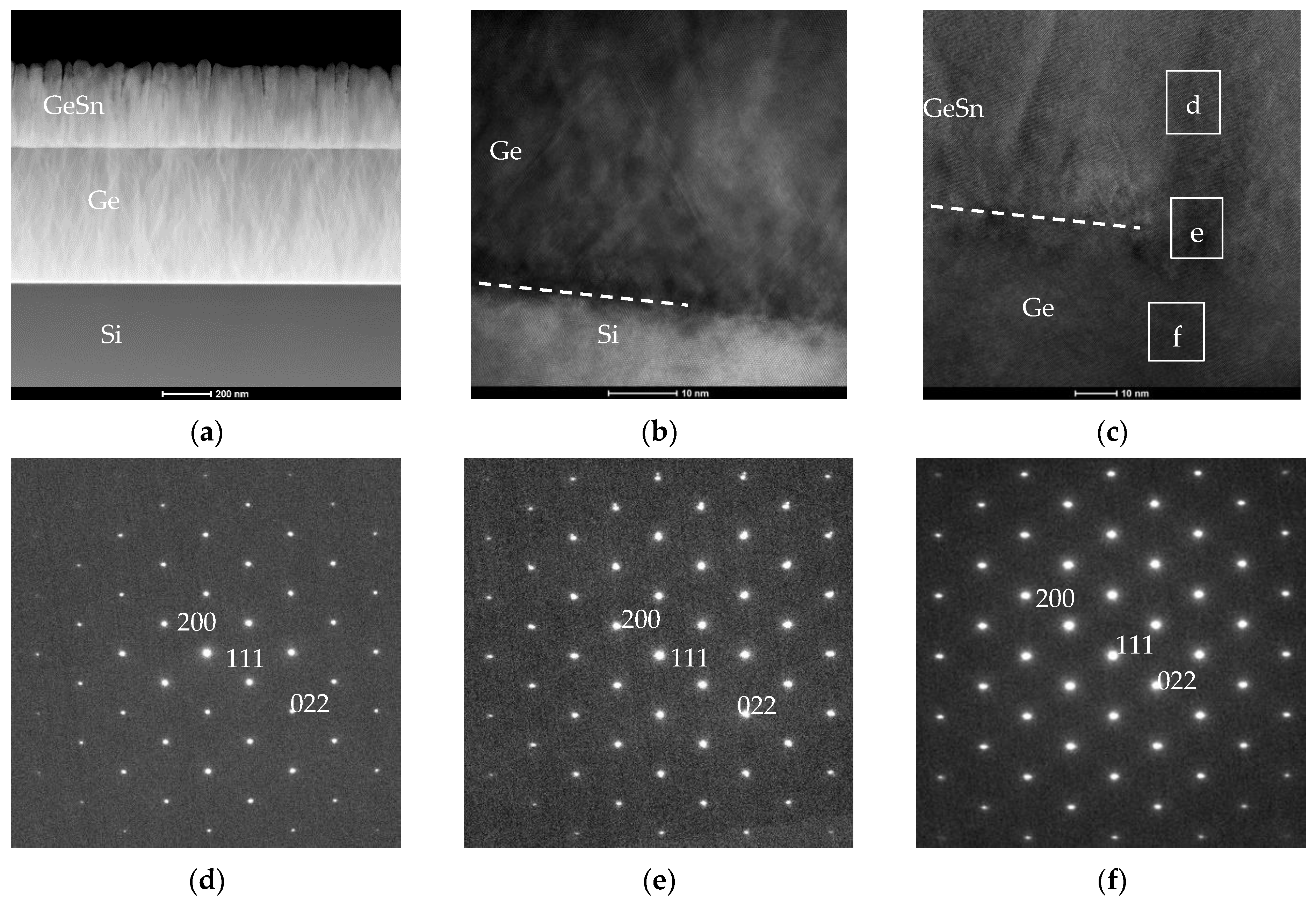
In order to further characterize the crystallinity, XTEM measurement was carried out on the Ge1−xSnx alloy film deposited at 240 °C. As shown in Figure 6a, the interfaces between Ge1−xSnx/Ge buffer/Si substrate were clear and recognizable. Figure 6b confirms the relaxation characteristics of the Ge buffer layer and clearly proves that the threading dislocations appear in the Ge buffer layer due to the mismatch between Ge and Si. In Figure 6c, the interface between the Ge1−xSnx/Ge buffer layer, atomic observation shows a highly ordered atomic arrangement in the interface. In Figure 6d–f is fast Fourier transformation (FFT) patterns of Ge1−xSnx, Ge1−xSnx/Ge buffer layer interface and Ge buffer layer. Diffraction spots are typical face-centered cubic [011] patterns, and clear lattice fringes of Ge and the Ge1−xSnx layer indicate that single-crystal films are grown by sputtering and the Ge1−xSnx layer is coherent with the Ge crystal.
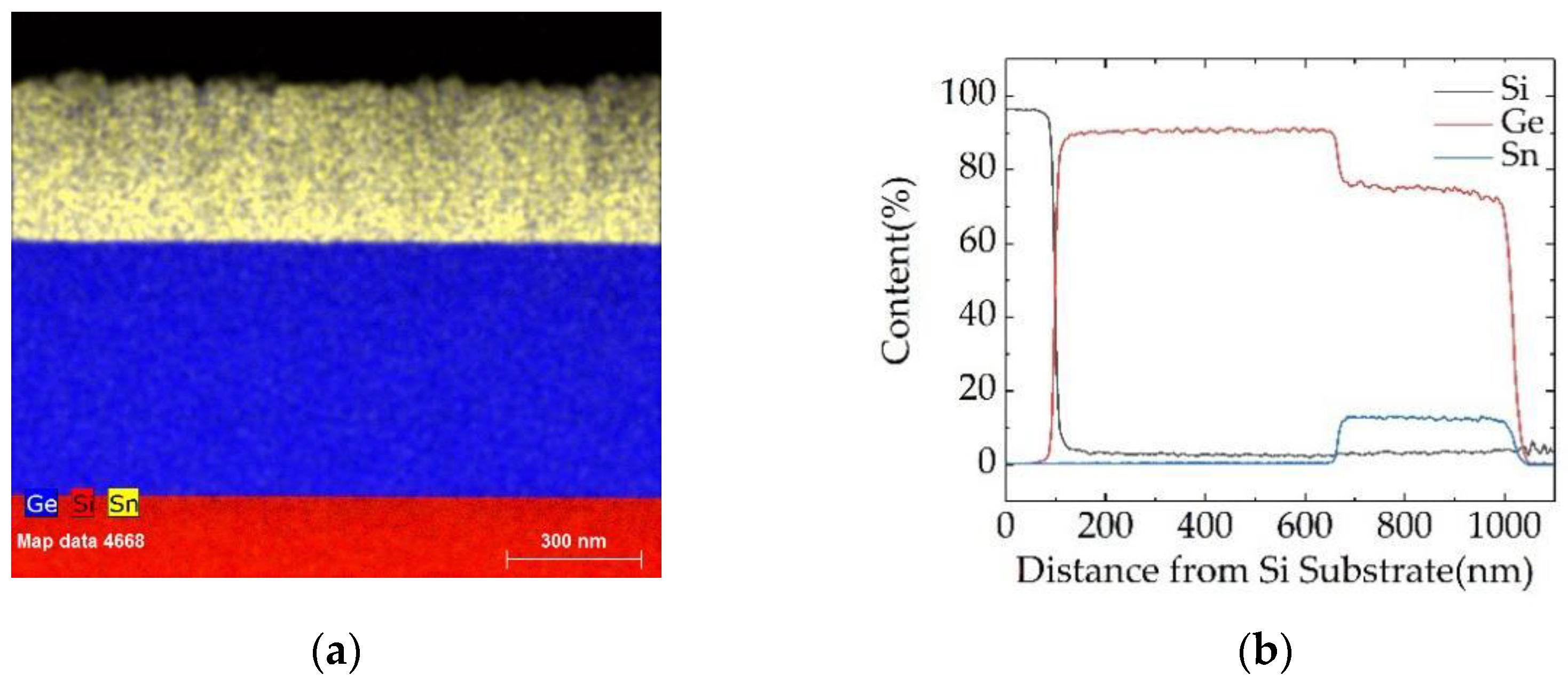
Electron dispersive X-ray (EDX) spectroscopy was performed to identify the elemental composition of the Ge and Ge1−xSnx films, and the results are shown in Figure 7. Figure 7a shows a spectral scan of the concentration values of uniformly distributed Sn, Ge and Si. Figure 7b shows the line scan of the concentration values of Sn, Ge and Si, where the Sn content (at%) is about 12.6–13.06%. According to the content distribution of Sn, there is no Sn segregation on the surface of the Ge1−xSnx film. Compared with references of single crystal Ge1−xSnx deposited by magnetron sputtering on silicon substrate, the tin content is the highest in this work, and the specific data are shown in Table 2.
In this work, Ge1−xSnx alloy thin films were prepared by a Ge–Sn co-sputtering principle, and the Ge target and Sn target were mounted on two targets, respectively. The sputtering power of Ge and Sn was controlled to achieve different atomic ratios of Sn. The temperature of the substrate can be adjusted. The higher the temperature, the higher the mobility energy of Sn atoms, and the easier it is to move to the appropriate position. Therefore, with the increase of temperature, Sn atoms occupied the position of Ge atoms forming a Ge1−xSnx alloy, and with the increase of temperature to 240 °C, the Sn doping peak was reached. When the temperature continued to rise, segregation occurred. When the temperature rose to 260 °C, segregation intensified, Sn atoms migrated to the surface of the sample, and the Sn content of Ge1−xSnx alloy decreased.
4. Conclusions
In this paper, the structural characteristics of Ge1−xSnx thin films at different substrate temperatures were studied in detail. XRD, Raman, TEM and AFM analysis showed that the coherent growth of Ge1−xSnx and Ge can be achieved by adjusting the substrate temperature, and the Sn content in the Ge1−xSnx film deposited at 240 °C was the highest, with the Sn content (at%) reaching 13%. These results show that single crystal Ge1−xSnx films can be grown on Si (001) wafer by sputtering at a temperature near the melting point of Sn, and its Sn content is the highest among GeSn prepared by sputtering on Si (001) substrate reported at present.
Author Contributions
Conceptualization, H.H., S.L., B.Z. and Z.Z.; methodology, H.H., S.L., B.Z. and Z.Z.; formal analysis, C.Q., J.H. and H.H.; visualization, C.Q., J.H. and H.H.; investigation, C.Q.; writing—original draft preparation, H.H.; writing—review and editing, H.H., D.Z. and S.L.; supervision, S.L.; project administration, S.L.; funding acquisition, S.L. All authors have read and agreed to the published version of the manuscript.
Funding
This research was funded by National Key R&D Program, grant number 2018YFB2003305.
Data Availability Statement
The data presented in this study are available within the manuscript.
Acknowledgments
The authors thank Platform for Characterization & Test of Suzhou Institute of Nano-Tech and Nano-Bionics (SINANO), Chinese Academy of Sciences (CAS) for the technical support.
Conflicts of Interest
The authors declare no conflict of interest.
References
- Tsai, C.H.; Lin, K.C.; Cheng, C.Y.; Lee, K.C.; Cheng, H.H.; Chang, G.E. GeSn lateral p-i-n waveguide photodetectors for mid-infrared integrated photonics. Opt. Lett. 2021, 46, 864–867. [Google Scholar] [CrossRef] [PubMed]
- Buzynin, Y.N.; Shengurov, V.G.; Denisov, S.A.; Yunin, P.A.; Chalkov, V.Y.; Drozdov, M.N.; Korolyov, S.A.; Nezhdanov, A.V. High Hole Mobility of Polycrystalline GeSn Layers Grown by Hot-Wire Chemical Vapor Deposition on Diamond Substrates. Phys. Status Solidi-Rapid Res. Lett. 2022, 16, 2100421. [Google Scholar] [CrossRef]
- Moto, K.; Yoshimine, R.; Suemasu, T.; Toko, K. Improving carrier mobility of polycrystalline Ge by Sn doping. Sci. Rep. 2018, 8, 14832. [Google Scholar] [CrossRef] [PubMed] [Green Version]
- Sau, J.D.; Cohen, M.L. Possibility of increased mobility in Ge-Sn alloy system. Phys. Rev. B 2007, 75, 045208. [Google Scholar] [CrossRef]
- Anas, E.; Dan, B.; Nils, V.D.D.; Konstantinos, P.; Gilles, P.; Nicolas, Z.; Etienne, H.; Xavier, C.; Sébastien, S.; Isabelle, S.; et al. Ultra-low-threshold continuous-wave and pulsed lasing in tensile-strained GeSn alloys. Nat. Photonics 2020, 14, 375–382. [Google Scholar]
- Uchida, N.; Hattori, J.; Lieten, R.R.; Ohishi, Y.; Takase, R.; Ishimaru, M.; Fukuda, K.; Maeda, T.; Locquet, J.P. Carrier and heat transport properties of poly-crystalline GeSn films for thin-film transistor applications. J. Appl. Phys. 2019, 126, 145105. [Google Scholar] [CrossRef]
- Zhang, L.; Hong, H.Y.; Yu, C.Y.; Li, C.; Chen, S.Y.; Huang, W.; Wang, J.Y.; Wang, H. Poly-GeSn Junctionless Thin-Film Transistors on Insulators Fabricated at Low Temperatures via Pulsed Laser Annealing. Phys. Status Solidi-Rapid Res. Lett. 2019, 13, 1900420. [Google Scholar] [CrossRef]
- Moto, K.; Yamamoto, K.; Imajo, T.; Suemasu, T.; Nakashima, H.; Toko, K. Sn Concentration Effects on Polycrystalline GeSn Thin Film Transistors. IEEE Electron Device Lett. 2021, 42, 1735–1738. [Google Scholar] [CrossRef]
- Mizoguchi, T.; Ishiyama, T.; Moto, K.; Imajo, T.; Suemasu, T.; Toko, K. Solid-Phase Crystallization of GeSn Thin Films on GeO2-Coated Glass. Phys. Status Solidi-Rapid Res. Lett. 2022, 16, 2100509. [Google Scholar] [CrossRef]
- Zhu, X.M.; Cui, M.; Wang, Y.; Yu, T.J.; Li, Q.Y.; Deng, J.X.; Gao, H.L. Evaluation of electricity generation on GeSn single-junction solar cell. Int. J. Energy Res. 2022, 1–8. [Google Scholar] [CrossRef]
- Wu, S.T.; Xu, S.Q.; Zhou, H.; Jin, Y.H.; Chen, Q.M.; Huang, Y.C.; Zhang, L.; Gong, X.; Tan, C.S. High-Performance Back-Illuminated Ge0.92Sn0.08/Ge Multiple-Quantum-Well Photodetector on Si Platform for SWIR Detection. IEEE J. Sel. Top. Quantum Electron. 2022, 28, 1–9. [Google Scholar] [CrossRef]
- Wang, N.; Xue, C.L.; Wan, F.S.; Zhao, Y.; Xu, G.Y.; Liu, Z.; Zheng, J.; Zuo, Y.H.; Cheng, B.W.; Wang, Q.M. High-Performance GeSn Photodetector Covering All Telecommunication Bands. IEEE Photonics J. 2021, 13, 1–9. [Google Scholar] [CrossRef]
- Tran, H.; Pham, T.; Margetis, J.; Zhou, Y.Y.; Dou, W.; Grant, P.C.; Grant, J.M.; Al-Kabi, S.; Sun, G.; Soref, R.A.; et al. Si-Based GeSn Photodetectors toward Mid-Infrared Imaging Applications. ACS Photonics 2019, 6, 2807–2815. [Google Scholar] [CrossRef] [Green Version]
- Zhang, L.F.; Shu, B.; Jiang, R.H.; Gao, Y.L.; Zhang, H.M.; Xuan, R.X.; Hu, H.Y. Short wave infrared LEDs based on strained GeSn. Micro Opt. Tech Lett. 2018, 60, 1151–1154. [Google Scholar] [CrossRef]
- Oehme, M.; Werner, J.; Gollhofer, M.; Schmid, M.; Kaschel, M.; Kasper, E.; Schulze, J. Room-Temperature Electroluminescence from GeSn Light-Emitting Pin Diodes on Si. IEEE Photonics Technol. Lett. 2011, 23, 1751–1753. [Google Scholar] [CrossRef]
- Zhou, Y.Y.; Dou, W.; Du, W.; Pham, T.; Ghetmiri, S.A.; Al-Kabi, S.; Mosleh, A.; Alher, M.; Margetis, J.; Tolle, J.; et al. Systematic study of GeSn heterostructure-based light-emitting diodes towards mid-infrared applications. J. Appl. Phys. 2016, 120, 023102. [Google Scholar] [CrossRef]
- Chang, C.; Li, H.; Huang, S.H.; Lin, L.C.; Cheng, H.H. Temperature-dependent electroluminescence from GeSn heterojunction light-emitting diode on Si substrate. Jpn. J. Appl. Phys. 2016, 55, 04EH03. [Google Scholar] [CrossRef]
- Kim, Y.; Assali, S.; Burt, D.; Jung, Y.; Joo, H.J.; Chen, M.; Ikonic, Z.; Moutanabbir, O.; Nam, D. Enhanced GeSn Microdisk Lasers Directly Released on Si. Adv. Opt. Mater. 2022, 10, 2101213. [Google Scholar] [CrossRef]
- Margetis, J.; Al-Kabi, S.; Du, W.; Dou, W.; Zhou, Y.Y.; Pham, T.; Grant, P.; Ghetmiri, S.; Mosleh, A.; Li, B.H.; et al. Si-Based GeSn Lasers with Wavelength Coverage of 2–3 μm and Operating Temperatures up to 180 K. ACS Photonics 2018, 5, 827–833. [Google Scholar] [CrossRef]
- Chang, G.-E.; Yu, S.-Q.; Liu, J.F.; Cheng, H.-H.; Soref, R.A.; Sun, G. Achievable Performance of Uncooled Homojunction GeSn Mid-Infrared Photodetectors. IEEE J. Sel. Top. Quantum Electron. 2022, 28, 1–11. [Google Scholar] [CrossRef]
- Kumar, H.; Basu, R. Effect of Defects on the Performance of Si-Based GeSn/Ge Mid-Infrared Phototransistors. IEEE Sens. J. 2021, 21, 5975–5982. [Google Scholar] [CrossRef]
- Zhou, Y.Y.; Ojo, S.; Wu, C.W.; Miao, Y.H.; Tran, H.; Grant, J.M.; Abernathy, G.; Amoah, S.; Bass, J.; Salamo, G.; et al. Electrically injected GeSn lasers with peak wavelength up to 2.7 μm. Photonics Res. 2022, 10, 222–229. [Google Scholar] [CrossRef]
- Asano, T.; Shimura, Y.; Nakatsuka, O.; Zaima, S. Influence of Sn incorporation and growth temperature on crystallinity of Ge1−xSnx layers heteroepitaxially grown on Ge(110) substrates. Thin Solid Film. 2013, 531, 504–508. [Google Scholar] [CrossRef]
- Chen, R.; Huang, Y.C.; Gupta, S.; Lin, A.C.; Sanchez, E.; Kim, Y.; Saraswat, K.C.; Kamins, T.I.; Harris, J.S. Material characterization of high Sn-content, compressively-strained GeSn epitaxial films after rapid thermal processing. J. Cryst. Growth 2013, 365, 29–34. [Google Scholar] [CrossRef]
- Trumbore, F.A. Solid Solubilities and Electrical Properties of Tin in Germanium Single Crystals. J. Electrochem. Soc. 1956, 103, 597–600. [Google Scholar] [CrossRef]
- Zheng, J.; Li, L.; Zhou, T.; Zuo, Y.; Li, C.; Cheng, B.; Wang, Q. Growth of Crystalline Ge1−xSnx Films on Si (100) by Magnetron Sputtering. ECS Solid State Lett. 2014, 3, 111–113. [Google Scholar] [CrossRef]
- Rathore, J.; Nanwani, A.; Mukherjee, S.; Das, S.; Moutanabbir, O.; Mahapatra, S. Composition uniformity and large degree of strain relaxation in MBE-grown thick GeSn epitaxial layers, containing 16% Sn. J. Phys. D Appl. Phys. 2021, 54, 185105. [Google Scholar] [CrossRef]
- Wei, L.; Miao, Y.; Pan, R.; Zhang, W.W.; Li, C.; Lu, H.; Chen, Y.F. Highly strained Ge1−xSnx alloy films with high Sn compositions grown by MBE. J. Cryst. Growth 2021, 557, 125996. [Google Scholar] [CrossRef]
- Wan, F.S.; Xu, C.; Wang, X.Y.; Xu, G.Y.; Cheng, B.W.; Xue, C.L. Study of strain evolution mechanism in Ge1_xSnx materials grown by low temperature molecular beam epitaxy. J. Cryst. Growth 2022, 577, 126399. [Google Scholar] [CrossRef]
- Olorunsola, O.; Said, A.; Ojo, S.; Abernathy, G.; Saha, S.; Wangila, E.; Grant, J.; Stanchu, H.; Acharya, S.; Du, W.; et al. Enhanced carrier collection efficiency of GeSn single quantum well towards all-group-IV photonics applications. J. Phys. D Appl. Phys. 2022, 55, 305101. [Google Scholar] [CrossRef]
- Kong, Z.Z.; Wang, G.L.; Liang, R.R.; Su, J.L.; Xun, M.; Miao, Y.H.; Gu, S.H.; Li, J.J.; Cao, K.H.; Lin, H.X.; et al. Growth and Strain Modulation of GeSn Alloys for Photonic and Electronic Applications. Nanomaterials 2022, 12, 981. [Google Scholar] [CrossRef] [PubMed]
- Grant, J.; Abernathy, G.; Olorunsola, O.; Ojo, S.; Amoah, S.; Wanglia, E.; Saha, S.K.; Sabbar, A.; Du, W.; Alher, M.; et al. Growth of Pseudomorphic GeSn at Low Pressure with Sn Composition of 16.7%. Materials 2021, 14, 7637. [Google Scholar] [CrossRef] [PubMed]
- Tsukamoto, T.; Hirose, N.; Kasamatsu, A.; Matsui, T.; Suda, Y. Effects of Low-Temperature GeSn Buffer Layers on Sn Surface Segregation During GeSn Epitaxial Growth. Electron. Mater. Lett. 2020, 16, 9–13. [Google Scholar] [CrossRef]
- Khelidj, H.; Portavoce, A.; Bertoglio, M.; Descoins, M.; Patout, L.; Hoummada, K.; Hallén, A.; Charaï, A.; Benoudia, M.C.; Mangelinck, D. Ge(Sn) growth on Si(001) by magnetron sputtering. Mater. Today Commun. 2021, 26, 101915. [Google Scholar] [CrossRef]
- Liu, X.Q.; Zheng, J.; Li, M.M.; Wan, F.S.; Niu, C.Q.; Liu, Z.; Zuo, Y.H.; Xue, C.L.; Cheng, B.W. Growth of relaxed GeSn film with high Sn content via Sn component-grade buffer layer structure. J. Phys. D Appl. Phys. 2021, 54, 435101. [Google Scholar] [CrossRef]
- Abdi, S.; Assali, S.; Atalla, M.R.M.; Koelling, S.; Warrender, J.M.; Moutanabbir, O. Recrystallization and interdiffusion processes in laser-annealed strain-relaxed metastable Ge0.89Sn0.11. J. Appl. Phys. 2022, 131, 105304. [Google Scholar] [CrossRef]
- Oka, H.; Mizubayashi, W.; Ishikawa, Y.; Uchida, N.; Mori, T.; Endo, K. Non-equilibrium solid-phase growth of amorphous GeSn layer on Ge-on-insulator wafer induced by flash lamp annealing. Appl. Phys. Express 2021, 14, 025505. [Google Scholar] [CrossRef]
- Cai, H.J.; Qian, K.; An, Y.Y.; Lin, G.Y.; Wu, S.S.; Ding, H.K.; Huang, W.; Chen, S.Y.; Wang, J.Y.; Li, C. Thickness-dependent behavior of strain relaxation and Sn segregation of GeSn epilayer during rapid thermal annealing. J. Alloys Compd. 2022, 904, 164068. [Google Scholar] [CrossRef]
- Wang, W.; Zhou, Q.; Dong, Y.; Tok, E.S.; Yeo, Y.-C. Critical thickness for strain relaxation of Ge1−xSnx (x ≤ 0.17) grown by molecular beam epitaxy on Ge(001). Appl. Phys. Lett. 2015, 106, 232106. [Google Scholar] [CrossRef]
- Lin, K.C.; Huang, P.R.; Li, H.; Cheng, H.H.; Chang, G.E. Temperature-dependent characteristics of GeSn/Ge multiple-quantum-well photoconductors on silicon. Opt. Lett. 2021, 46, 3604–3607. [Google Scholar] [CrossRef]
- Assali, S.; Nicolas, J.; Moutanabbir, O. Enhanced Sn incorporation in GeSn epitaxial semiconductors via strain relaxation. J. Appl. Phys. 2019, 125, 025304. [Google Scholar] [CrossRef]
- Dou, W.; Benamara, M.; Mosleh, A.; Margetis, J.; Grant, P.; Zhou, Y.Y.; Al-Kabi, S.; Du, W.; Tolle, J.; Li, B.H.; et al. Investigation of GeSn Strain Relaxation and Spontaneous Composition Gradient for Low-Defect and High-Sn Alloy Growth. Sci. Rep. 2018, 8, 5640. [Google Scholar] [CrossRef] [PubMed] [Green Version]
- Joe, M.; Yu, S.-Q.; Nupur, B.; Li, B.H.; Du, W.; John, T. Strain engineering in epitaxial Ge1−xSnx: A path towards low-defect and high Sn-content layers. Semicond. Sci. Technol. 2017, 32, 124006. [Google Scholar]
- Zheng, J.; Liu, Z.; Zhang, Y.W.; Zuo, Y.H.; Li, C.B.; Xue, C.L.; Cheng, B.W.; Wang, Q.M. Growth of high-Sn content (28%) GeSn alloy films by sputtering epitaxy. J. Cryst. Growth 2018, 492, 29–34. [Google Scholar] [CrossRef]
- Dev, S.; Khiangte, K.R.; Lodha, S. Wafer-scale mono-crystalline GeSn alloy on Ge by sputtering and solid phase epitaxy. J. Phys. D-Appl. Phys. 2020, 53, 21LT01. [Google Scholar] [CrossRef]
- Qian, L.; Tong, J.C.; Suo, F.; Liu, L.; Fan, W.J.; Luo, Y.; Zhang, D.H. GeSn/GaAs Hetero-Structure by Magnetron Sputtering. IEEE J. Quantum Electron. 2020, 56, 1–5. [Google Scholar] [CrossRef]
- Abdel-Rahman, M.; Alduraibi, M.; Hezam, M.; Ilahi, B. Sputter deposited GeSn alloy: A candidate material for temperature sensing layers in uncooled microbolometers. Infrared Phys. Technol. 2019, 97, 376–380. [Google Scholar] [CrossRef]
- Zhang, L.; Wang, Y.S.; Chen, N.L.; Lin, G.Y.; Li, C.; Huang, W.; Chen, S.Y.; Xu, J.F.; Wang, J.Y. Raman scattering study of amorphous GeSn films and their crystallization on Si substrates. J. Non-Cryst. Solids 2016, 448, 74–78. [Google Scholar] [CrossRef]
- Tsukamoto, T.; Hirose, N.; Kasamatsu, A.; Mimura, T.; Matsui, T.; Suda, Y. Formation of GeSn layers on Si (001) substrates at high growth temperature and high deposition rate by sputter epitaxy method. J. Mater. Sci. 2015, 50, 4366–4370. [Google Scholar] [CrossRef]
- Miao, Y.H.; Wang, Y.B.; Hu, H.Y.; Liu, X.Y.; Su, H.; Zhang, J.; Yang, J.Y.; Tang, Z.H.; Wu, X.; Song, J.J.; et al. Characterization of crystalline GeSn layer on tensile-strained Ge buffer deposited by magnetron sputtering. Mater. Sci. Semicond. Process. 2018, 85, 134–140. [Google Scholar] [CrossRef]
- Gencarelli, F.; Vincent, B.; Demeulemeester, J.; Vantomme, A.; Moussa, A.; Franquet, A.; Kumar, A.; Bender, H.; Meersschaut, J.; Vandervorst, W.; et al. Crystalline Properties and Strain Relaxation Mechanism of CVD Grown GeSn. ECS J. Solid State Sci. Technol. 2013, 2, P134–P137. [Google Scholar] [CrossRef]
- D’Costa, V.R.; Tolle, J.; Roucka, R.; Poweleit, C.D.; Kouvetakis, J.; Menéndez, J. Raman scattering in Ge1−ySny alloys. Solid State Commun. 2007, 144, 240–244. [Google Scholar] [CrossRef]
- Su, S.; Wang, W.; Cheng, B.W.; Hu, W.X.; Zhang, G.Z.; Xue, C.L.; Zuo, Y.H.; Wang, Q.M. The contributions of composition and strain to the phonon shift in alloys. Solid State Commun. 2011, 151, 647–650. [Google Scholar] [CrossRef]
Figure 1.
Ge1−xSnx co-sputtering schematic diagram.
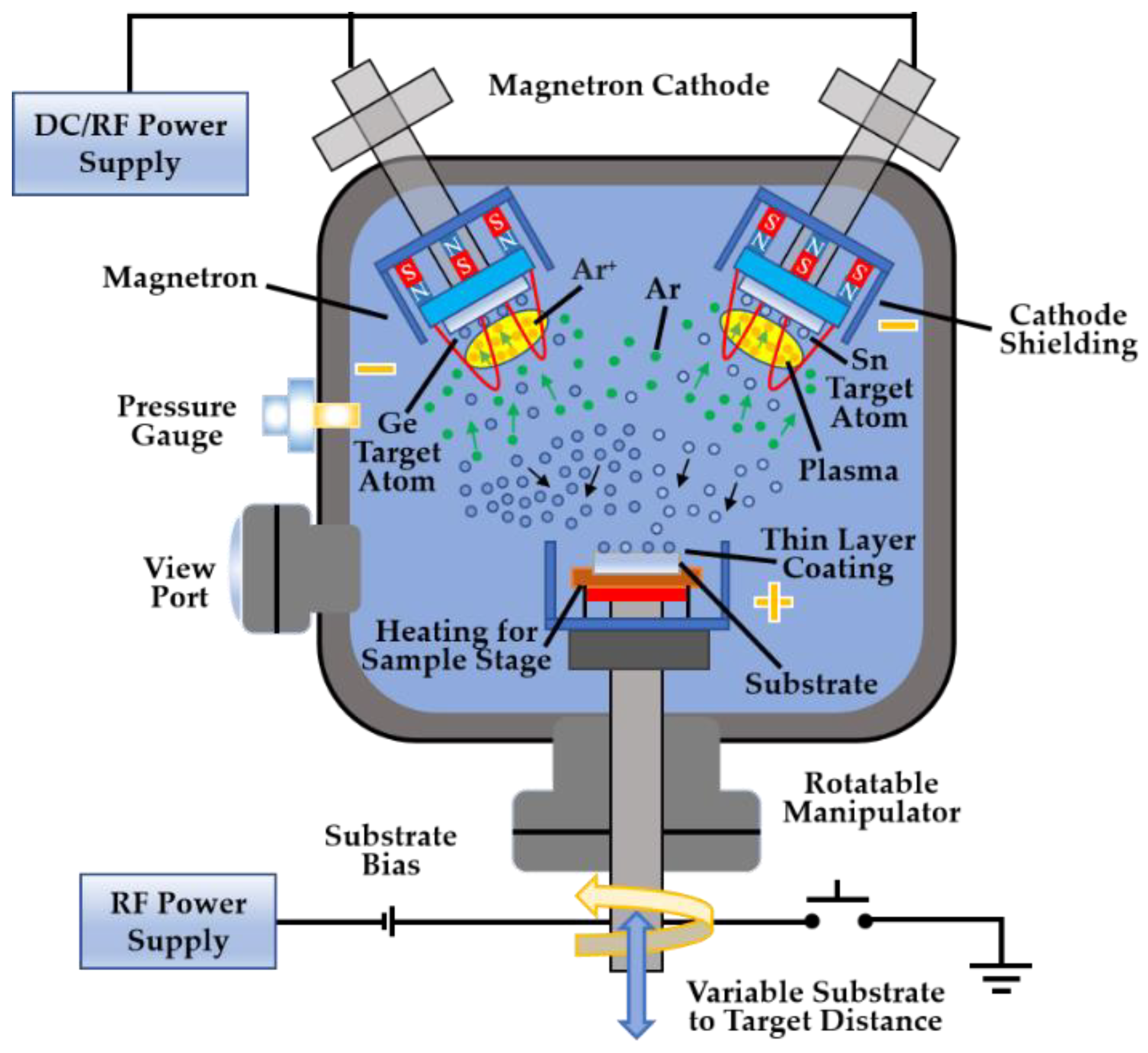
Figure 2.
HR-XRD 2θ-ω scans of the Ge1−xSnx films on Si (100) for different deposited temperatures: (a) (004); (b) (224).
Figure 2.
HR-XRD 2θ-ω scans of the Ge1−xSnx films on Si (100) for different deposited temperatures: (a) (004); (b) (224).
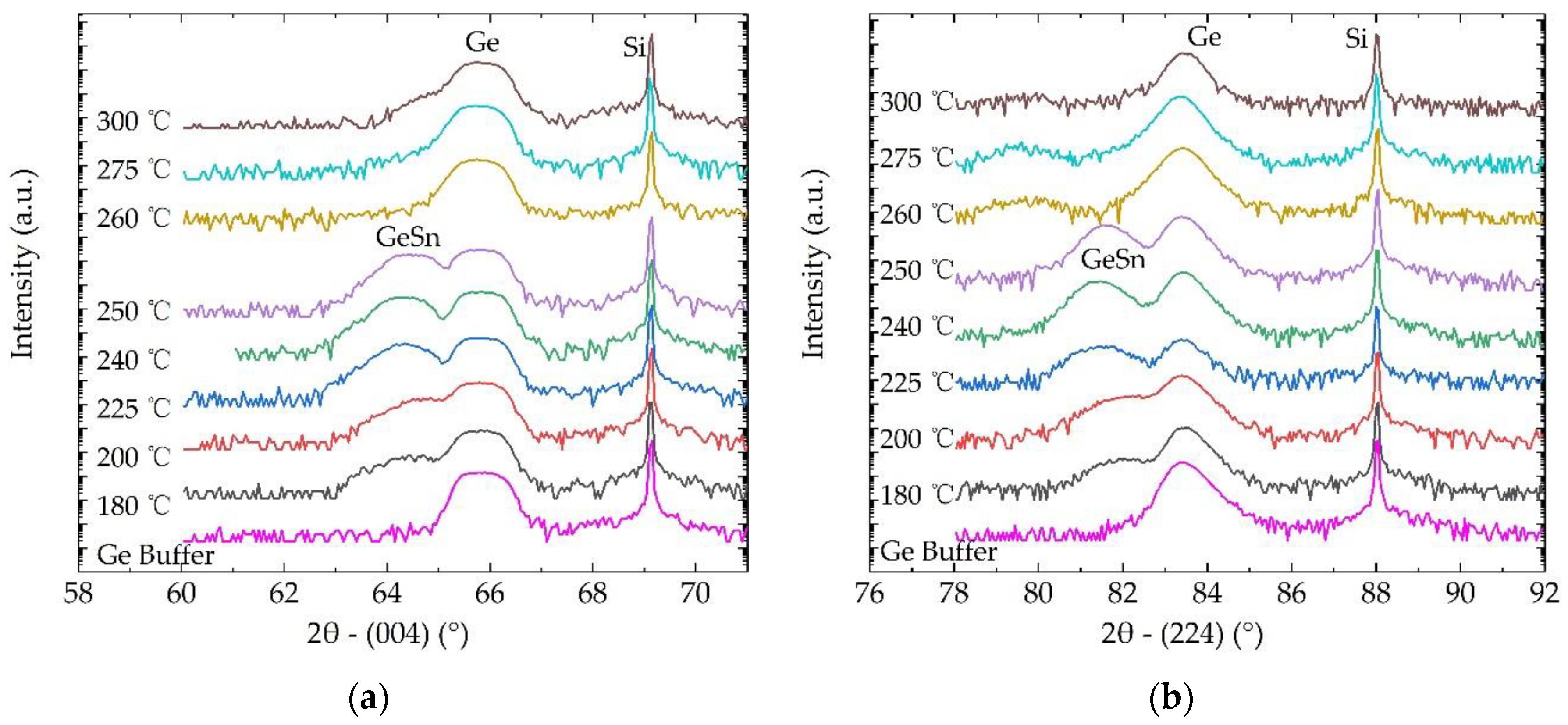
Figure 3.
Ge-Ge Raman spectra of Ge1−xSnx layers with different growth temperature.

Figure 4.
AFM images were obtained from the Ge buffer layer and Ge1−xSnx samples at different deposition temperatures: (a) Ge Buffer; (b) Ge1−xSnx deposited at 180 °C; (c) Ge1−xSnx deposited at 200 °C; (d) Ge1−xSnx deposited at 225 °C; (e) Ge1−xSnx deposited at 240 °C; (f) Ge1−xSnx deposited at 250 °C; (g) Ge1−xSnx deposited at 260 °C; (h) Ge1−xSnx deposited at 275 °C; (i) Ge1−xSnx deposited at 300 °C.

Figure 5.
Comparison of surface roughness between the Ge buffer layer and Ge1−xSnx samples deposited at different temperatures.
Figure 5.
Comparison of surface roughness between the Ge buffer layer and Ge1−xSnx samples deposited at different temperatures.

Figure 6.
XTEM images of Ge1−xSnx film deposited at 240 °C: (a) full view of the film by scanning TEM; (b) high resolution TEM at Ge/Si interface; (c) high resolution TEM at Ge/Ge1−xSnx interface; (d–f) show the FFT patterns corresponding to the various regions in (c).
Figure 6.
XTEM images of Ge1−xSnx film deposited at 240 °C: (a) full view of the film by scanning TEM; (b) high resolution TEM at Ge/Si interface; (c) high resolution TEM at Ge/Ge1−xSnx interface; (d–f) show the FFT patterns corresponding to the various regions in (c).

Figure 7.
EDX of the sample with Ge1−xSnx film as deposited at 240 °C, (a) map scanning; (b) line scanning.
Figure 7.
EDX of the sample with Ge1−xSnx film as deposited at 240 °C, (a) map scanning; (b) line scanning.


Table 1.
Out-of-plane () lattice constants, in-plane () lattice constants, unstrained lattice constants (), measured Sn content (xm), degree of strain relaxation (R) and in-plane strain () of the Ge1−xSnx samples.
Table 1.
Out-of-plane () lattice constants, in-plane () lattice constants, unstrained lattice constants (), measured Sn content (xm), degree of strain relaxation (R) and in-plane strain () of the Ge1−xSnx samples.
| Growth Temperature (°C) | (nm) | (nm) | (nm) | xm (%) | R (%) | (%) |
|---|---|---|---|---|---|---|
| 180 | 0.57702 | 0.56998 | 0.57399 | 9.98 | 41.1 | −0.007 |
| 200 | 0.57676 | 0.56990 | 0.57381 | 10.25 | 40.9 | −0.007 |
| 225 | 0.57860 | 0.57688 | 0.57786 | 14.29 | 91 | −0.002 |
| 240 | 0.57871 | 0.57738 | 0.57813 | 15.38 | 93.2 | −0.001 |
| 250 | 0.57826 | 0.57616 | 0.57735 | 13.79 | 88.2 | −0.002 |
Publisher’s Note: MDPI stays neutral with regard to jurisdictional claims in published maps and institutional affiliations. |
© 2022 by the authors. Licensee MDPI, Basel, Switzerland. This article is an open access article distributed under the terms and conditions of the Creative Commons Attribution (CC BY) license (https://creativecommons.org/licenses/by/4.0/).
Share and Cite
MDPI and ACS Style
Huang, H.; Zhao, D.; Qi, C.; Huang, J.; Zeng, Z.; Zhang, B.; Lu, S. Effect of Growth Temperature on Crystallization of Ge1−xSnx Films by Magnetron Sputtering. Crystals 2022, 12, 1810. https://doi.org/10.3390/cryst12121810
AMA Style
Huang H, Zhao D, Qi C, Huang J, Zeng Z, Zhang B, Lu S. Effect of Growth Temperature on Crystallization of Ge1−xSnx Films by Magnetron Sputtering. Crystals. 2022; 12(12):1810. https://doi.org/10.3390/cryst12121810
Chicago/Turabian StyleHuang, Hongjuan, Desheng Zhao, Chengjian Qi, Jingfa Huang, Zhongming Zeng, Baoshun Zhang, and Shulong Lu. 2022. "Effect of Growth Temperature on Crystallization of Ge1−xSnx Films by Magnetron Sputtering" Crystals 12, no. 12: 1810. https://doi.org/10.3390/cryst12121810
Note that from the first issue of 2016, this journal uses article numbers instead of page numbers. See further details here.