

Properties of SiC and Si3N4 Thin Films Containing Self-Assembled Gold Nanoparticles

 , ,
, , 
Abstract
1. Introduction
2. Materials and Methods
3. Results and Discussion
3.1. Structural Properties of the Films
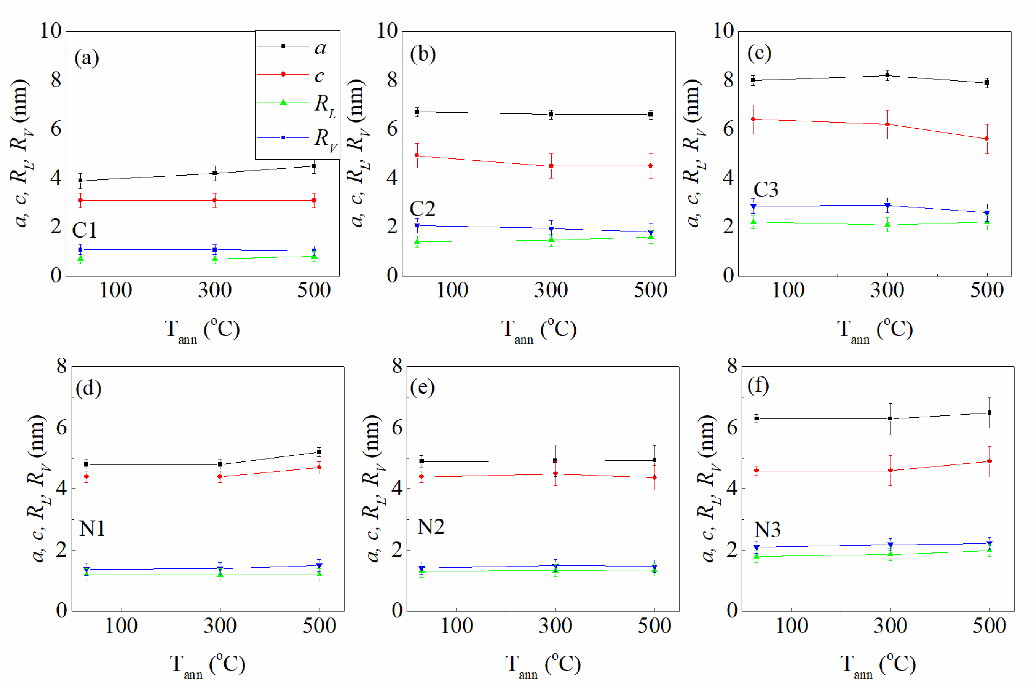
3.1.1. Nanoparticle Formation and Their Size-Arrangement Properties
3.1.2. Nanoparticle Internal Structure–Crystalline Properties
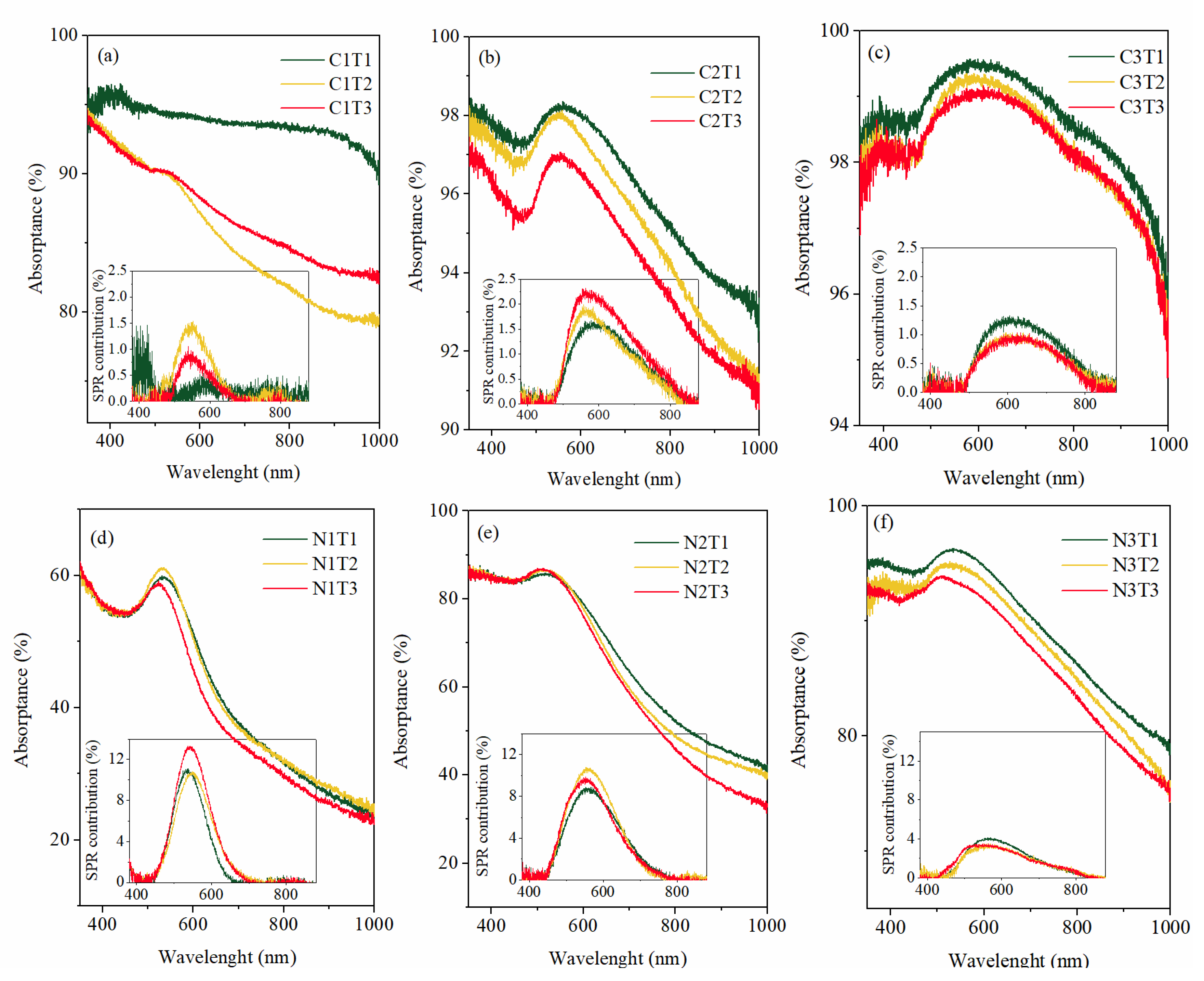
3.2. Optical Properties of the Films
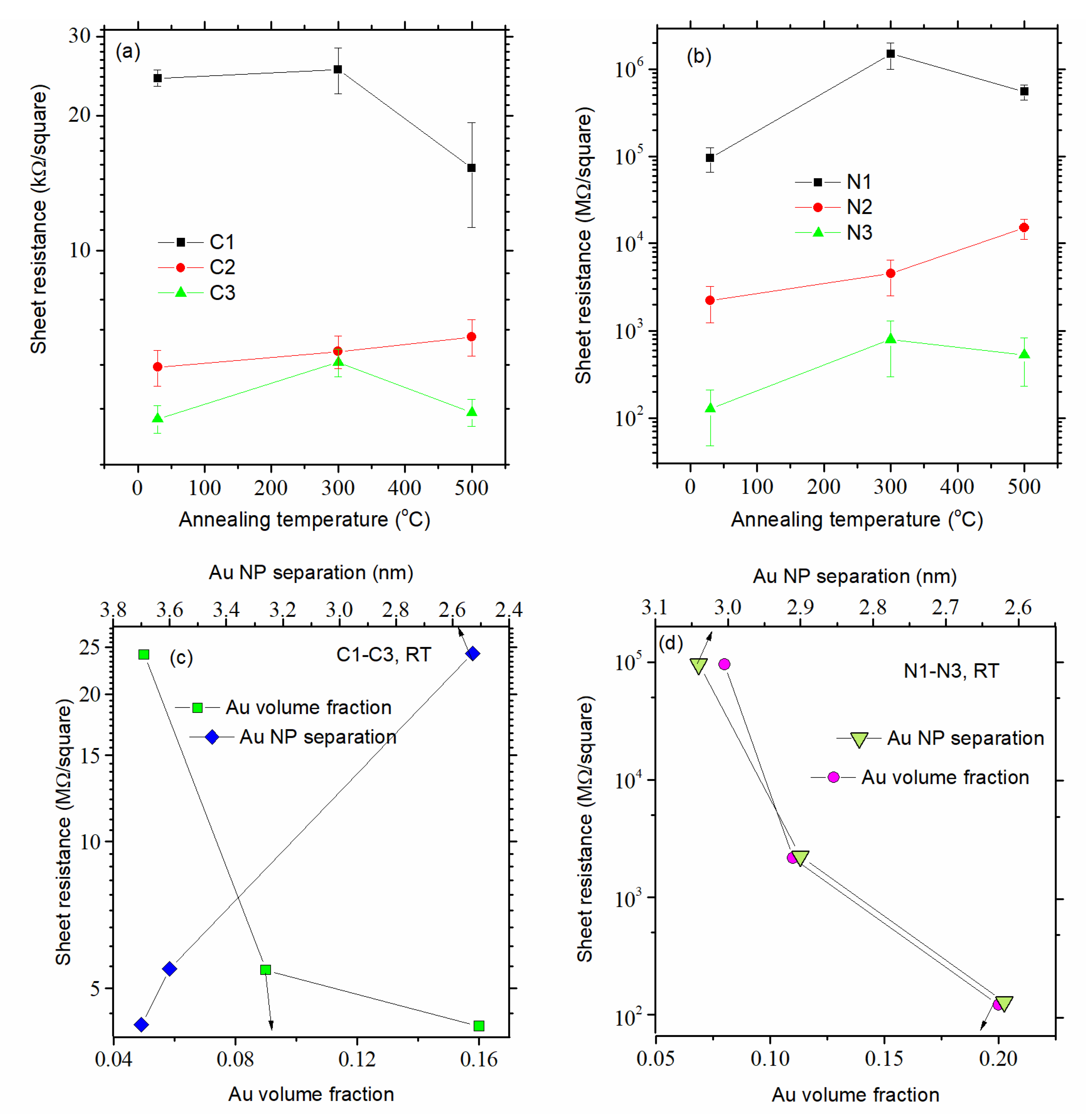
3.3. Electrical Properties of the Films
4. Conclusions
Author Contributions
Funding
Data Availability Statement
Acknowledgments
Conflicts of Interest
References
- Kim, J.H.; Chung, K.W. Microstructure and properties of silicon nitride thin films deposited by reactive bias magnetron sputtering. J. Appl. Phys. 1998, 83, 5831–5839. [Google Scholar] [CrossRef]
- Zhang, S.; Raniero, L.; Fortunato, E.; Pereira, L.; Martins, N.; Canhola, P.; Ferreira, I.; Nedev, N.; Águas, H.; Martins, R. Characterization of silicon carbide thin films prepared by VHF-PECVD technology. J. Non-Cryst. Solids 2004, 338–340, 530–533. [Google Scholar] [CrossRef]
- Tehrani, F.S.; Fakhredin, M.; Tafreshi, M.J. The optical properties of silicon carbide thin films prepared by HWCVD from pure silane and methane under various total gas partial pressure. Mater. Res. Express 2019, 6, 086469. [Google Scholar] [CrossRef]
- Morkoç, H.; Strite, S.; Gao, G.B.; Lin, M.E.; Sverdlov, B.; Burns, M. Large-band-gap SiC, III-V nitride, and II-VI ZnSe-based semiconductor device technologies. J. Appl. Phys. 1994, 76, 1363–1398. [Google Scholar] [CrossRef]
- Lattemann, M.; Nold, E.; Ulrich, S.; Leiste, H.; Holleck, H. Investigation and characterisation of silicon nitride and silicon carbide thin films. Surf. Coat. Technol. 2003, 174–175, 365–369. [Google Scholar] [CrossRef]
- Choi, S.R.; Kim, D.; Choa, S.-H.; Lee, S.-H.; Kim, J.-K. Thermal Conductivity of AlN and SiC Thin Films. Int. J. Thermophys. 2006, 27, 896–905. [Google Scholar] [CrossRef]
- Su, G.-P.; Zheng, X.-H.; Qiu, L.; Tang, D.-W.; Zhu, J. Measurement of Thermal Conductivity of Anisotropic SiC Crystal. Int. J. Thermophys. 2013, 34, 2334–2342. [Google Scholar] [CrossRef]
- Liu, A.Y.; Cohen, M.L. Structural properties and electronic structure of low-compressibility materials: β-Si3N4 and hypothetical β-Si3N4. Phys. Rev. B 1990, 41, 10727–10734. [Google Scholar] [CrossRef]
- Vila, M.; Cáceres, D.; Prieto, C. Mechanical properties of sputtered silicon nitride thin films. J. Appl. Phys. 2003, 94, 7868. [Google Scholar] [CrossRef]
- Zhang, X.; Grigoropoulos, C.P. Thermal conductivity and diffusivity of free-standing silicon nitride thin films. Rev. Sci. Instrum. 1995, 66, 1115–1120. [Google Scholar] [CrossRef]
- Brassard, D.; el Khakani, M.A. Dielectric properties of amorphous hydrogenated silicon carbide thin films grown by plasma-enhanced chemical vapor deposition. J. Appl. Phys. 2003, 93, 4066–4071. [Google Scholar] [CrossRef]
- Zhou, J.; Zheng, X. Structure and electronic properties of SiC thin-films deposited by RF magnetron sputtering. Trans. Nonferrous Met. Soc. China 2007, 17, 373–377. [Google Scholar] [CrossRef]
- Ledermann, N.; Baborowski, J.; Muralt, P.; Xantopoulos, N.; Tellenbach, J.-M. Sputtered silicon carbide thin films as protective coating for MEMS applications. Surf. Coat. Technol. 2000, 125, 246–250. [Google Scholar] [CrossRef]
- Bhatt, V.; Chandra, S. Silicon Nitride Films Deposited by RF Sputtering for Microstructure Fabrication in MEMS. J. Elec. Mater. 2009, 38, 1979–1989. [Google Scholar] [CrossRef]
- Isoird, K.; Lazar, M.; Ottaviani, L.; Locatelli, M.L.; Raynaud, C.; Planson, D.; Chante, J.P. Study of 6H–SiC high voltage bipolar diodes under reverse biases. Appl. Surf. Sci. 2001, 184, 477–482. [Google Scholar] [CrossRef]
- Dow, H.S.; Kim, W.S.; Lee, J.W. Thermal and electrical properties of silicon nitride substrates. AIP Adv. 2017, 7, 095022. [Google Scholar] [CrossRef]
- Solzbacher, F.; Imawan, C.; Steffes, H.; Obermeier, E.; Eickhoff, M. A highly stable SiC based microhotplate NO2 gas-sensor. Sens. Actuators B Chemical. 2001, 78, 216–220. [Google Scholar] [CrossRef]
- Kaloyeros, A.E.; Jové, F.A.; Goff, J.; Arkles, B. Review—Silicon Nitride and Silicon Nitride-Rich Thin Film Technologies: Trends in Deposition Techniques and Related Applications. ECS J. Solid State Sci. Technol. 2017, 6, P691–P714. [Google Scholar] [CrossRef]
- Miranzo, P.; García, E.; Ramírez, C.; González-Julián, J.; Belmonte, M.; Osendi, M.I. Anisotropic thermal conductivity of silicon nitride ceramics containing carbon nanostructures. J. Eur. Ceram. Soc. 2012, 32, 1847–1854. [Google Scholar] [CrossRef]
- Taube, W.R.; Kumar, A.; Saravanan, R.; Agarwal, P.B.; Kothari, P.; Joshi, B.C.; Kumar, D. Efficiency enhancement of silicon solar cells with silicon nanocrystals embedded in PECVD silicon nitride matrix. Sol. Energy Mater. Sol. Cells 2012, 101, 32–35. [Google Scholar] [CrossRef]
- Kim, S.-H.; Jang, K.; Kang, P.W.; Ahn, J.-P.; Seol, J.-B.; Kwak, C.-M.; Hatzoglou, C.; Vurpillot, F.; Choi, P.-P. Characterization of Pd and Pd@Au core-shell nanoparticles using atom probe tomography and field evaporation simulation. J. Alloys Compd. 2020, 831, 154721. [Google Scholar] [CrossRef]
- Huo, N.; Kang, J.; Wei, Z.; Li, S.-S.; Li, J.; Wei, S.-H. Novel and Enhanced Optoelectronic Performances of Multilayer MoS2-WS2 Heterostructure Transistors. Adv. Funct. Mater. 2014, 24, 7025–7031. [Google Scholar] [CrossRef]
- Johannesson, D.; Nawaz, M.; Jacobs, K.; Norrga, S.; Nee, H.-P. Potential of ultra-high voltage silicon carbide semiconductor devices. In Proceedings of the 2016 IEEE 4th Workshop on Wide Bandgap Power Devices and Applications (WiPDA), Fayetteville, AR, USA, 7–9 November 2016; pp. 253–258. [Google Scholar] [CrossRef]
- Lagier, T.; Ladoux, P.; Dworakowski, P. Potential of silicon carbide MOSFETs in the DC/DC converters for future HVDC offshore wind farms. High Volt. 2017, 2, 233–243. [Google Scholar] [CrossRef]
- Nazarkovsky, M.; Alekseev, S.; Huczko, A.; Zaitsev, V.; Dupont, J.; Kai, J.; Xing, Y.; Scofield, A.L.; Chacón, G.; Carreira, R.S. Structural and photocatalytic properties of silicon carbide powder and nanowires modified by gold nanoparticles. Res. Chem. Intermed. 2019, 45, 4081–4100. [Google Scholar] [CrossRef]
- Klemm, H. Silicon Nitride for High-Temperature Applications: Silicon Nitride for High-Temperature Applications. J. Am. Ceram. Soc. 2010, 93, 1501–1522. [Google Scholar] [CrossRef]
- Kaloyeros, A.E.; Pan, Y.; Goff, J.; Arkles, B. Review—Silicon Nitride and Silicon Nitride-Rich Thin Film Technologies: State-of-the-Art Processing Technologies, Properties, and Applications. ECS J. Solid State Sci. Technol. 2020, 9, 063006. [Google Scholar] [CrossRef]
- Rajendran, R.; Shrestha, L.K.; Minami, K.; Subramanian, M.; Jayavel, R.; Ariga, K. Dimensionally integrated nanoarchitectonics for a novel composite from 0D, 1D, and 2D nanomaterials: RGO/CNT/CeO2 ternary nanocomposites with electrochemical performance. J. Mater. Chem. A 2014, 2, 18480–18487. [Google Scholar] [CrossRef]
- Bernstorff, S.; Holý, V.; Endres, J.; Valeš, V.; Sobota, J.; Siketić, Z.; Bogdanović-Radović, I.; Buljan, M.; Dražić, G. Co nanocrystals in amorphous multilayers—A structure study. J. Appl. Crystallogr. 2013, 46, 1711–1721. [Google Scholar] [CrossRef]
- Zhu, S.; Song, Y.; Zhao, X.; Shao, J.; Zhang, J.; Yang, B. The photoluminescence mechanism in carbon dots (graphene quantum dots, carbon nanodots, and polymer dots): Current state and future perspective. Nano Res. 2015, 8, 355–381. [Google Scholar] [CrossRef]
- Nekić, N.; Šarić, I.; Salamon, K.; Basioli, L.; Sancho-Parramon, J.; Grenzer, J.; Hübner, R.; Bernstorff, S.; Petravić, M.; Mičetić, M. Preparation of non-oxidized Ge quantum dot lattices in amorphous Al2O3, Si3N4 and SiC matrices. Nanotechnology 2019, 30, 335601. [Google Scholar] [CrossRef]
- Melanko, J.B.; Pearce, M.E.; Salem, A.K. Nanotubes, Nanorods, Nanofibers, and Fullerenes for Nanoscale Drug Delivery. In Nanotechnology in Drug Delivery; de Villiers, M.M., Aramwit, P., Kwon, G.S., Eds.; Springer: New York, NY, USA, 2009; pp. 105–127. [Google Scholar] [CrossRef]
- Balázsi, C.; Wéber, F.; Kövér, Z.; Shen, Z.; Kónya, Z.; Kasztovszky, Z.; Vértesy, Z.; Biró, L.P.; Kiricsi, I.; Arató, P. Application of carbon nanotubes to silicon nitride matrix reinforcements. Curr. Appl. Phys. 2006, 6, 124–130. [Google Scholar] [CrossRef]
- Basioli, L.; Tkalčević, M.; Bogdanović-Radović, I.; Dražić, G.; Nadazdy, P.; Siffalovic, P.; Salamon, K.; Mičetić, M. 3D Networks of Ge Quantum Wires in Amorphous Alumina Matrix. Nanomaterials 2020, 10, 1363. [Google Scholar] [CrossRef] [PubMed]
- Borges, J.; Buljan, M.; Sancho-Parramon, J.; Bogdanović-Radović, I.; Siketić, Z.; Scherer, T.; Kübel, C.; Bernstorff, S.; Cavaleiro, A.; Vaz, F.; et al. Evolution of the surface plasmon resonance of Au:TiO2 nanocomposite thin films with annealing temperature. J. Nanopart. Res. 2014, 16, 2790. [Google Scholar] [CrossRef]
- Amendola, V.; Pilot, R.; Frasconi, M.; Maragò, O.M.; Iatì, M.A. Surface plasmon resonance in gold nanoparticles: A review. J. Phys. Condens. Matter 2017, 29, 203002. [Google Scholar] [CrossRef]
- Yao, G.-Y.; Liu, Q.-L.; Zhao, Z.-Y. Studied Localized Surface Plasmon Resonance Effects of Au Nanoparticles on TiO2 by FDTD Simulations. Catalysts 2018, 8, 236. [Google Scholar] [CrossRef]
- Haes, A.J.; van Duyne, R.P. A Nanoscale Optical Biosensor: Sensitivity and Selectivity of an Approach Based on the Localized Surface Plasmon Resonance Spectroscopy of Triangular Silver Nanoparticles. J. Am. Chem. Soc. 2002, 124, 10596–10604. [Google Scholar] [CrossRef]
- Huang, X.; El-Sayed, I.H.; Qian, W.; El-Sayed, M.A. Cancer Cell Imaging and Photothermal Therapy in the Near-Infrared Region by Using Gold Nanorods. J. Am. Chem. Soc. 2006, 128, 2115–2120. [Google Scholar] [CrossRef]
- Hirsch, L.R.; Stafford, R.J.; Sershen, S.R.; Halas, N.J.; Hazle, J.D.; West, J.L. Nanoshell-assisted tumor ablation using near infrared light under magnetic resonance guidance. Proc. Natl. Acad. Sci. USA 2003, 100, 113549-54. [Google Scholar] [CrossRef]
- Dykman, L.A.; Khlebtsov, N.G. Gold Nanoparticles in Biology and Medicine: Recent Advances and Prospects. Acta Nat. 2011, 3, 34–55. [Google Scholar] [CrossRef]
- Qian, H.; Pretzer, L.A.; Velazquez, J.C.; Zhao, Z.; Wong, M.S. Gold nanoparticles for cleaning contaminated water: Gold nanoparticles for cleaning contaminated water. J. Chem. Technol. Biotechnol. 2013, 88, 735–741. [Google Scholar] [CrossRef]
- Martins, P.; Kappert, S.; Le, H.N.; Sebastian, V.; Kühn, K.; Alves, M.; Pereira, L.; Cuniberti, G.; Melle-Franco, M.; Lanceros-Méndez, S. Enhanced Photocatalytic Activity of Au/TiO2 Nanoparticles against Ciprofloxacin. Catalysts 2020, 10, 234. [Google Scholar] [CrossRef]
- Atwater, H.A.; Polman, A. Plasmonics for Improved Photovoltaic Devices. Nat. Mater. 2010, 9, 205–213. [Google Scholar] [CrossRef] [PubMed]
- Car, T.; Jakovac, I.; Šarić, I.; Bernstorff, S.; Micetic, M. Structural, Optical and Electrical Properties of Al+MoO3 and Au+MoO3 Thin Films Prepared by Magnetron Codeposition. Materials 2021, 14, 766. [Google Scholar] [CrossRef]
- Okumu, J.; Dahmen, C.; Sprafke, A.N.; Luysberg, M.; von Plessen, G.; Wuttig, M. Photochromic silver nanoparticles fabricated by sputter deposition. J. Appl. Phys. 2005, 97, 094305. [Google Scholar] [CrossRef]
- Hatakeyama, Y.; Onishi, K.; Nishikawa, K. Effects of sputtering conditions on formation of gold nanoparticles in sputter deposition technique. RSC Adv. 2011, 1, 1815–1821. [Google Scholar] [CrossRef]
- Van der Pauw, L.J.A. A method of measuring the resistivity and Hall coefficient on lamellae of arbitrary shape. Philips Tech. Rev. 1958, 26, 220–224. [Google Scholar]
- Buljan, M.; Radić, N.; Bernstorff, S.; Dražić, G.; Bogdanović-Radović, I.; Holý, V. Grazing-incidence small-angle X-ray scattering: Application to the study of quantum dot lattices. Acta Crystallogr. Found Crystallogr. 2012, 68, 124–138. [Google Scholar] [CrossRef]
- Basioli, L.; Salamon, K.; Tkalčević, M.; Mekterović, I.; Bernstorff, S.; Mičetić, M. Application of GISAXS in the Investigation of Three-Dimensional Lattices of Nanostructures. Crystals 2019, 9, 479. [Google Scholar] [CrossRef]
- Buljan, M.; Radić, N.; Ivanda, M.; Bogdanović-Radović, I.; Karlušić, M.; Grenzer, J.; Prucnal, S.; Dražić, G.; Pletikapić, G.; Svetličić, V.; et al. Ge quantum dot lattices in Al2O3 multilayers. J. Nanoparticle Res. 2013, 15, 1485. [Google Scholar] [CrossRef]
- Pinto, S.R.C.; Rolo, A.G.; Buljan, M.; Chahboun, A.; Bernstorff, S.; Barradas, N.P.; Alves, E.; Kashtiban, R.J.; Bangert, U.; Gomes, M.J.M. Low-temperature fabrication of layered self-organized Ge clusters by RF sputtering. Nanoscale Res. Lett. 2011, 6, 341. [Google Scholar] [CrossRef]
- Buljan, M.; Radić, N.; Sancho-Paramon, J.; Janicki, V.; Grenzer, J.; Bogdanović-Radović, I.; Siketić, Z.; Ivanda, M.; Utrobičić, A.; Hübner, R.; et al. Production of three-dimensional quantum dot lattice of Ge/Si core–shell quantum dots and Si/Ge layers in an alumina glass matrix. Nanotechnology 2015, 26, 065602. [Google Scholar] [CrossRef] [PubMed]
- Nekić, N.; Parramon, J.S.; Bogdanović-Radović, I.; Grenzer, J.; Huebner, R.; Ivanda, M.; Buljan, M. Ge/Si core/shell quantum dots in alumina: Tuning the optical absorption by the core and shell size. Nanophotonics 2017, 6, 1055–1062. [Google Scholar] [CrossRef][Green Version]
- Musumeci, P.; Reitano, R.; Calcagno, L.; Roccaforte, F.; Makhtari, A.; Grimaldi, M.G. Relaxation and crystallization of amorphous silicon carbide probed by optical measurements. Philos. Mag. B 1997, 76, 323–333. [Google Scholar] [CrossRef]
- Jain, P.K.; Lee, K.S.; El-Sayed, I.H.; El-Sayed, M.A. Calculated Absorption and Scattering Properties of Gold Nanoparticles of Different Size, Shape, and Composition: Applications in Biological Imaging and Biomedicine. J. Phys. Chem. B 2006, 110, 7238–7248. [Google Scholar] [CrossRef] [PubMed]
- Scholl, J.A.; Koh, A.L.; Dionne, J.A. Quantum plasmon resonances of individual metallic nanoparticles. Nature 2012, 483, 421–427. [Google Scholar] [CrossRef]
- Singhal, R.; Kabiraj, D.; Kulriya, P.K.; Pivin, J.C.; Chandra, R.; Avasthi, D.K. Blue-Shifted SPR of Au Nanoparticles with Ordering of Carbon by Dense Ionization and Thermal Treatment. Plasmonics 2013, 8, 295–305. [Google Scholar] [CrossRef]
- Nair, K.; Mitra, S.S. Electrical properties and hopping transport in amorphous silicon carbide films. J. Non-Cryst. Solids 1977, 24, 1–17. [Google Scholar] [CrossRef]
- Anwar, M.S.; Bukhari, S.Z.A.; Ha, J.H.; Lee, J.; Song, I.-H.; Kim, Y.-W. Controlling the electrical resistivity of porous silicon carbide ceramics and their applications: A review. Int. J. Appl. Ceram. Technol. 2022, 19, 1814–1840. [Google Scholar] [CrossRef]
- Choi, W. Optical, structural, and electrical properties of amorphous silicon carbide films. In Silicon-Based Material and Devices; Elsevier: Amsterdam, The Netherlands, 2001; pp. 1–71. [Google Scholar] [CrossRef]
- Fujita, S.; Sasaki, A. Dangling Bonds in Memory-Quality Silicon Nitride Films. J. Electrochem. Soc. 1985, 132, 398–402. [Google Scholar] [CrossRef]
- Zhou, D.; Huang, L.; Yuan, J.; Li, C. Influences of different sputtering current on the microstructure and electrical properties of silicon nitride thin films deposited on cemented carbide tools. Ceram. Int. 2021, 47, 32160–32167. [Google Scholar] [CrossRef]


| Sample/Par | (W) | (°C) | Au to SiC Volume Ratio | Sample/Par | (W) | (°C) | Au to Si3N4 Volume Ratio |
|---|---|---|---|---|---|---|---|
| C1T1 | 1 | --- | 0.05 | N1T1 | 1 | --- | 0.08 |
| C1T2 | 1 | 300 | 0.05 | N1T2 | 1 | 300 | 0.08 |
| C1T3 | 1 | 500 | 0.05 | N1T3 | 1 | 500 | 0.08 |
| C2T1 | 3 | --- | 0.09 | N2T1 | 3 | --- | 0.11 |
| C2T2 | 3 | 300 | 0.1 | N2T2 | 3 | 300 | 0.11 |
| C2T3 | 3 | 500 | 0.1 | N2T3 | 3 | 500 | 0.12 |
| C3T1 | 5 | --- | 0.16 | N3T1 | 5 | --- | 0.2 |
| C3T2 | 5 | 300 | 0.15 | N3T2 | 5 | 300 | 0.2 |
| C3T3 | 5 | 500 | 0.17 | N3T3 | 5 | 500 | 0.2 |
| Sample/Par | |||||||||
|---|---|---|---|---|---|---|---|---|---|
| C1T1 | 3.9 ± 0.3 | 3.9 ± 0.3 | 1.2 ± 0.2 | 1.0 ± 0.2 | 1.5 ± 0.2 | 0.9 ± 0.1 | 0.9 ± 0.2 | 1.0 ± 0.2 | 0.23 ± 0.08 |
| C1T2 | 4.2 ± 0.3 | 4.2 ± 0.3 | 1.3 ± 0.2 | 1.1 ± 0.2 | 1.4 ± 0.2 | 0.9 ± 0.1 | 0.8 ± 0.2 | 1.1 ± 0.2 | 0.24 ± 0.07 |
| C1T3 | 4.5 ± 0.3 | 4.5 ± 0.3 | 1.4 ± 0.2 | 1.1 ± 0.2 | 1.5 ± 0.2 | 1.0 ± 0.1 | 0.8 ± 0.2 | 1.0 ± 0.2 | 0.23 ± 0.08 |
| C2T1 | 6.8 ± 0.2 | 4.8 ± 0.5 | 2.6 ± 0.2 | 2.2 ± 0.2 | 2.3 ± 0.2 | 1.7 ± 0.1 | 1.4 ± 0.2 | 2.1 ± 0.3 | 0.49 ± 0.08 |
| C2T2 | 6.6 ± 0.2 | 4.5 ± 0.5 | 2.7 ± 0.2 | 1.9 ± 0.3 | 2.2 ± 0.3 | 1.9 ± 0.2 | 1.5 ± 0.2 | 2.3 ± 0.3 | 0.48 ± 0.09 |
| C2T3 | 6.6 ± 0.2 | 4.5 ± 0.5 | 2.7 ± 0.3 | 2.2 ± 0.2 | 2.0 ± 0.3 | 1.7 ± 0.1 | 1.6 ± 0.3 | 2.0 ± 0.4 | 0.48 ± 0.08 |
| C3T1 | 7.8 ± 0.2 | 6.9 ± 0.6 | 3.0 ± 0.3 | 1.7 ± 0.3 | 2.1 ± 0.3 | 2.2 ± 0.3 | 2.1 ± 0.3 | 2.7 ± 0.3 | 0.56 ± 0.08 |
| C3T2 | 8.5 ± 0.2 | 6.5 ± 0.6 | 3.1 ± 0.3 | 1.9 ± 0.3 | 2.1 ± 0.3 | 2.3 ± 0.3 | 2.1 ± 0.3 | 2.9 ± 0.3 | 0.56 ± 0.08 |
| C3T3 | 8.7 ± 0.2 | 6.2 ± 0.6 | 3.4 ± 0.3 | 2.3 ± 0.3 | 2.1 ± 0.3 | 2.2 ± 0.3 | 2.1 ± 0.3 | 2.3 ± 0.4 | 0.57 ± 0.09 |
| N1T1 | 4.8 ± 0.2 | 4.4 ± 0.2 | 1.4 ± 0.2 | 1.9 ± 0.2 | 2.1 ± 0.2 | 1.3 ± 0.2 | 1.2 ± 0.2 | 1.4 ± 0.2 | 0.18 ± 0.04 |
| N1T2 | 4.8 ± 0.2 | 4.4 ± 0.2 | 1.5 ± 0.2 | 2.2 ± 0.2 | 1.9 ± 0.2 | 1.3 ± 0.2 | 1.2 ± 0.2 | 1.4 ± 0.2 | 0.18 ± 0.04 |
| N1T3 | 5.2 ± 0.2 | 4.4 ± 0.2 | 1.4 ± 0.2 | 2.3 ± 0.2 | 1.9 ± 0.2 | 1.3 ± 0.2 | 1.2 ± 0.2 | 1.5 ± 0.2 | 0.18 ± 0.04 |
| N2T1 | 4.9 ± 0.2 | 4.5 ± 0.2 | 1.6 ± 0.2 | 1.8 ± 0.2 | 1.9 ± 0.2 | 1.3 ± 0.1 | 1.3 ± 0.2 | 1.4 ± 0.2 | 0.19 ± 0.05 |
| N2T2 | 4.9 ± 0.5 | 4.5 ± 0.4 | 1.6 ± 0.4 | 2.5 ± 0.4 | 1.8 ± 0.3 | 1.4 ± 0.2 | 1.3 ± 0.2 | 1.5 ± 0.2 | 0.19 ± 0.04 |
| N2T3 | 4.9 ± 0.5 | 5.3 ± 0.4 | 1.6 ± 0.4 | 3.3 ± 0.4 | 1.8 ± 0.3 | 1.8 ± 0.3 | 1.4 ± 0.2 | 1.5 ± 0.2 | 0.19 ± 0.04 |
| N3T1 | 6.3 ± 0.2 | 4.6 ± 0.2 | 1.4 ± 0.1 | 2.0 ± 0.2 | 2.0 ± 0.2 | 1.3 ± 0.2 | 1.7 ± 0.2 | 2.1 ± 0.2 | 0.31 ± 0.05 |
| N3T2 | 6.3 ± 0.5 | 4.6 ± 0.5 | 1.8 ± 0.4 | 3.4 ± 0.4 | 1.4 ± 0.4 | 1.8 ± 0.4 | 1.9 ± 0.2 | 2.2 ± 0.2 | 0.33 ± 0.06 |
| N3T3 | 6.4 ± 0.5 | 4.9 ± 0.5 | 1.2 ± 0.4 | 1.2 ± 0.2 | 1.4 ± 0.4 | 1.8 ± 0.4 | 2.0 ± 0.2 | 2.2 ± 0.2 | 0.34 ± 0.06 |
| Par/Sample | |||||||||
|---|---|---|---|---|---|---|---|---|---|
| Peak pos. (nm) | 590 ± 4 | 544 ± 2 | 542 ± 2 | 586 | 567 | 562 | 620 | 620 | 620 |
| FWHM (nm) | 132 | 102 | 96 | 197 | 184 | 210 | 254 | 255 | 255 |
| Peak max. (%) | 0.5 | 1.0 | 1.5 | 1.5 | 1.9 | 2.2 | 1.3 | 1.0 | 1.0 |
| Par/Sample | |||||||||
| Peak pos. (nm) | 537 | 550 | 541 | 560 | 555 | 558 | 570 | 570 | 549 |
| FWHM (nm) | 101 | 107 | 111 | 157 | 150 | 148 | 200 | 201 | 211 |
| Peak max. (%) | 10.8 | 10.7 | 13.0 | 8.8 | 9.8 | 10.6 | 4.0 | 3.3 | 3.3 |
Publisher’s Note: MDPI stays neutral with regard to jurisdictional claims in published maps and institutional affiliations. |
© 2022 by the authors. Licensee MDPI, Basel, Switzerland. This article is an open access article distributed under the terms and conditions of the Creative Commons Attribution (CC BY) license (https://creativecommons.org/licenses/by/4.0/).
Share and Cite
Isaković, S.; Đekić, M.; Tkalčević, M.; Boršćak, D.; Periša, I.; Bernstorff, S.; Mičetić, M. Properties of SiC and Si3N4 Thin Films Containing Self-Assembled Gold Nanoparticles. Crystals 2022, 12, 1361. https://doi.org/10.3390/cryst12101361
Isaković S, Đekić M, Tkalčević M, Boršćak D, Periša I, Bernstorff S, Mičetić M. Properties of SiC and Si3N4 Thin Films Containing Self-Assembled Gold Nanoparticles. Crystals. 2022; 12(10):1361. https://doi.org/10.3390/cryst12101361
Chicago/Turabian StyleIsaković, Senad, Maja Đekić, Marija Tkalčević, Denis Boršćak, Ivana Periša, Sigrid Bernstorff, and Maja Mičetić. 2022. "Properties of SiC and Si3N4 Thin Films Containing Self-Assembled Gold Nanoparticles" Crystals 12, no. 10: 1361. https://doi.org/10.3390/cryst12101361
APA StyleIsaković, S., Đekić, M., Tkalčević, M., Boršćak, D., Periša, I., Bernstorff, S., & Mičetić, M. (2022). Properties of SiC and Si3N4 Thin Films Containing Self-Assembled Gold Nanoparticles. Crystals, 12(10), 1361. https://doi.org/10.3390/cryst12101361