Article

Implementation of Method for Studying the Thermal Conductivity of Perovskite Thin Films

by
Mariya Aleksandrova
1,*,
Ivailo Pandiev
2 and
Ajaya Kumar Singh
3,4
1
Department of Microelectronics, Technical University of Sofia, 1000 Sofia, Bulgaria
2
Department of Electronics, Technical University of Sofia, 1000 Sofia, Bulgaria
3
Department of Chemistry, Govt. V.Y.T.PG. Autonomous College Durg, Chhattisgarh 491001, India
4
School of Chemistry & Physics, Westville Campus, University of KwaZulu-Natal, Durban 4000, South Africa
*
Author to whom correspondence should be addressed.
Crystals 2022, 12(10), 1326; https://doi.org/10.3390/cryst12101326
Submission received: 30 August 2022 / Revised: 13 September 2022 / Accepted: 16 September 2022 / Published: 20 September 2022
(This article belongs to the Section Materials for Energy Applications)

Abstract

:
In this paper, an approach for precise determination of the thermal conductivity of novel lead-free perovskite thin films by method, realized with a field programmable analog array circuit, is presented. The objective of the work is to study the relation between the thermal conductivity of the photoelectric perovskites and the thermal stability of the solar cells, in which they are incorporated. It is found that the solar cells’ long-term stability under different exploitation conditions, such as continuous illumination and elevated temperatures, is affected to a different extent, according to the thermal conductivity. The developed setup for implementation of the method is adapted for thin-film samples and can be applied to all layers involved in the solar cell, thus defining their individual contribution to the overall device thermal degradation. According to the conducted measurements, the coefficients of thermal conductivity for the novel materials are as follows: for the iodine-based perovskite film, it is 0.14 W/mK and for the chlorine-based perovskite film, it is 0.084 W/mK. As a result, the thermal instability and degradation rate at continuous illumination are, respectively, 10.6% and 200 nV/min for the iodine-based perovskite solar cell, and 6.5% and 20 nV/min for the chlorine-based cell. At elevated temperatures up to 54 °C, the corresponding instability values are 15 µV/°C with a degradation rate of an average of 2.2 µV/min for the cell with iodine-containing perovskite and 300 nV/°C with a degradation rate of 66 nV/min for the cell with chlorine-containing perovskite.

1. Introduction

Recently, perovskite solar cells have been of great interest due to their excellent ratio of compactness to efficiency, easy tailoring of the sunlight absorption coefficient in a broad wavelength range, and possibility for low-cost, large-area processing. They belong to the generation of thin-film cells which are low-cost, because less material is consumed for the photoelectric absorber and the substrate [1]. The first candidates in this group have been CdTe and CIGS, exhibiting efficiency greater than 20%, but their commercialization has been limited due to the rare or hazardous chemical components in their composition. The perovskite solar cells, as a representative of thin-film photovoltaic technology, possess the same advantages. Additionally, as compared to conventional technology, they can respond to a broad range of wavelengths according to their composition and respective band gap. Possibility for fabrication on different substrates, including foils and textile has opened the doors to various portable applications [2]. It should be mentioned that the researchers’ efforts have been directed to further increasing the efficiency of perovskite solar cells by tailoring the metallization system, e.g., by application of metallic nanoparticles, strengthening the photons absorption and at the same time reduce the device temperature, facilitating the dissipation of accumulated heat [3,4].
In line with the trend for eco-friendly fabrication process, thus far, the efforts have been focused on the synthesis of lead-free perovskites, which are a relatively new class of materials with a great potential to replace conventional lead-containing perovskites [5]. One of the greatest challenges for their commercialization is still the great thermal instability of lead-free perovskite solar cells, which strongly affects their open circuit photovoltage. The most efficient approach to improve the thermal properties of the perovskites is by chemical engineering, including doping by less thermally sensitive elements [6], or composite with conducting polymers [7]. Device engineering is also possible by insertion of additional films around the photoelectric one playing a role of thermal insulators, and also UV and moisture blocking layers [8,9]. However, any additionally inserted layer caused optical and/or electrical losses due to the light dissipation, or interfacial contact resistance, respectively. Thus, although suitable approaches have been elaborated to enhance the thermal stability, when a new photoelectric substance is applied, it is always important to precisely determine its thermal conductivity and to evaluate its individual contribution to the overall thermal and electrical performance of the device.
The thermal conductivity of the photo absorbing layers in solar cells is one of the very important factors affecting the performance of the cells, because the absorbed heat can change the band gap of the semiconductor and its charge carrier’s mobility. It has been previously found that the internal temperature increases as a result of strong light or ambient temperature raising, and results in defects formation, such as microvoids appearing, films cracking, and delamination at the layers’ interfaces [10,11]. This leads to photovoltage decay and electrical and mechanical instability of the device. Thermal conduction occurs because of phonons transfer and charge carriers’ movement (mainly electrons). The materials that have a high coefficient of thermal conductivity absorb and dissipate more heat to the neighboring layers; therefore the risk of cells’ degradation is higher if such films are incorporated into the structure. Then, it is important to know the materials’ thermal characteristics during their selection, especially when novel films are implemented.
To measure the coefficient of thermal conductivity of each thin film in the solar cells, the well-known three-omega () method has been applied [12,13,14]. This technique relies on a strip-shaped material microfabricated on a thermally insulating substrate and serving as a resistive heater. At switching on a source of AC current with a frequency of ω to the contact pads of the strip, the periodic heating generates oscillations in the electrical resistance of the material at a frequency of . A voltage drop across the strip occurs and its third harmonic () is used to estimate the magnitude of the temperature oscillations, and thus to analyze the thermal properties of the strip material. The thermally insulating substrate is usually sapphire and the measurement of the 3rd harmonic should be conducted in an air evacuated chamber to avoid thermal losses and heat circulation, as the entire thermal field should be concentrated over the microstrip.
There are some advantages related to the application of the method, especially when studying various types of thin films in a vacuum environment. For example, when using the method, a blackbody is not used in the measurement process and, as a result, there is no infrared radiation. At the same time, the long equilibration times, sometimes lasting several hours, used in this type of high temperature measurements employing standard measuring techniques, are reduced to several periods of temperature oscillations over the sample (for example, thin film metal wire or semiconductor line), at most a few seconds. Thus, precise control of the chamber temperature for hours is not necessary for the method. The measured data can be obtained by slowly heating or cooling the sample [12].
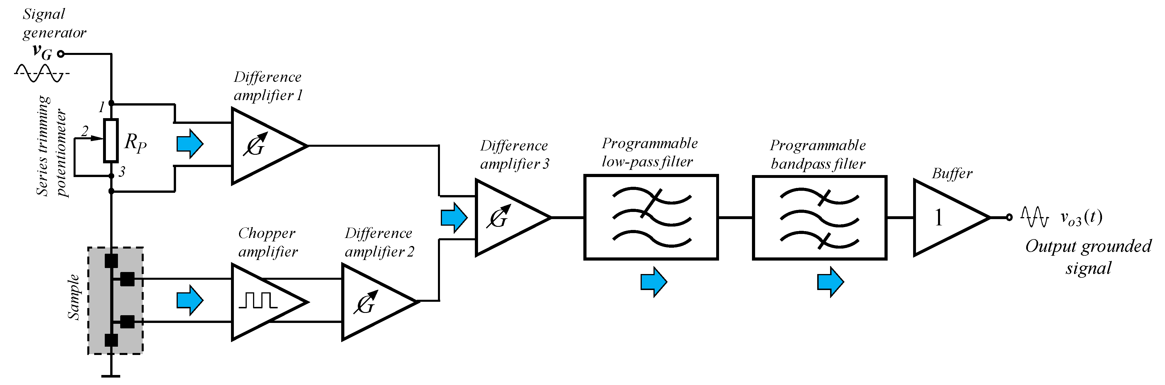
In this study, the three-omega method was adapted to serve as an indirect source of information for the thermal behavior of lead-free perovskite materials. This method relies on a specific topology of the perovskite layers, forming a heat concentrator over a wire of the material after passing an alternating current with ω frequency, causing in this way resistive component variation. The amplitude of the third harmonic of the voltage Vm3 over the wire-patterned component is used for calculation of the basic thermal coefficients [15]. Additionally, the stability of the photovoltage vs. time at maximum illumination and stability vs. temperature at constant illumination was also investigated for full stability characterization of the samples and to study the connection between materials’ thermal conductivity and the stability of the solar cell, implementing these materials. To the best of the authors’ knowledge, this is the first time application of the method, realized by field programmable analog array (FPAA) for extraction of information about the thermal conductivity of chlorine and iodine-based lead-free perovskite solar materials. The results are important for gaining new knowledge about the behavior of materials, unexplored from a thermal point of view. They are helpful to establish limitations, coming from the exploitation conditions, related to heat dissipation in thin-film solar cell (e.g., due to ambient temperature increase or ultimate exposure to intensive light). To the best of the authors’ knowledge, this method is used for first time for any kind of perovskite solar cells. The most widely used method reported in the literature for determination of the thermal conductivity is scanning near-field thermal microscopy which, however, suffers from disadvantages such as a difficult understanding of the origin of the contrast in the images obtained, how to quantify the physical properties of the materials investigated based on the image and the low scan rate for high resolution image [16,17]. There are no such drawbacks at the 3-omega method, which is based on direct relation between current and resistance, their frequency and temperature dependences, regardless of the surface type.

2. Theoretical and Experimental Methods

2.1. Fundametals of the 3ω Method

For realization of the method, the heat concentrator from Figure 1 is used [18,19].
In the case of sinusoidal heating, the temperature T over the thermal concentrator (the microstripped material) consists of time t and spatially Z-dependent components [20].
T ( z ; t ) = T z e x p ( i 2 ω t )
Considering the heat diffusion equation, it can be written that
d 2 T z d z 2 i 2 ω α T z ,  
where α is the thermal diffusivity. Regarding the spatial component to the substrate, where z > 0, it is
T z = T 0 e x p ( q z ) ,
where q is the wavenumber of the thermal wave. The time-dependent periodic temperature for the sample can be expressed as
T ( z , t ) = T 0 e x p ( i 2 ω t q z )
The oscillating power of the heater can be written
P 0   cos ( 2 ω t ) = P 0 ϕ ( e x p ( i 2 ω t ) )
Taking into account the microstrip area A and the expression for heat flux ϕ, the following equation can be obtained:
P 0 A e x p ( i 2 ω t ) = k T 0 2 ω α exp ( i 2 ω t + i π 4 ) ,
where k is Boltzmann constant. From Equation (6) T 0 can be expressed and then for the temperature oscillations can be written:
T ( z ; t ) = P 0 A 2 ω c p k e x p ( i 2 ω t i π 4 q z ) ,
where cp is thermal capacity of the material. The next step is to determine the effect of the oscillative temperature on the resistance of the microstrip, considering the real part of Equation (7) just below the microstrip where z = 0:
R ( t ) = R 0 ( 1 + β Δ T d c + β Δ T a c cos ( 2 ω t + π 4 ) ,
where β is the thermal coefficient of resistance, Δ T d c is the temperature variation at DC conditions and Δ T a c is the magnitude of the AC temperature oscillations.
As the voltage across the microstrip is a product of the microstrip resistance and the input current, then:
V ( t ) = I 0 R 0 ( ( 1 + β Δ T d c ) cos ( ω t ) + 1 2 β Δ T a c + 1 2 β Δ T a c cos ( 3 ω t + π 4 ) )
where I 0 R 0   = V 0 and the phase shift is obtained because of multiplying the 2 ω term in the resistance with the ω of the input current oscillation.
Finally, for the voltage at frequency 3 ω is obtained:
V 3 ω = 1 2 V 0 β Δ T a c
In the case of thin films, the geometrical sizes (thickness t, length l, and width b) of the microstrip are crucial for concentration of the heat in the material and get measurable noise-reduced signal. Then, the temperature oscillation in the film can be expressed as:
Δ T f = P 0 t 2 b l Λ ,
where Λ is the thermal conductivity of the material of interest (in our case the perovskite materials), which can be expressed from the Equation (11).
Λ = P 0 t 2 b l ( Δ T Δ T s ) ,
where ΔTs is the thermal response of the substrate.
For practical realization of this principle, a lock-in amplifier was designed, capable of measuring the basic frequency and the third harmonic simultaneously. In the present paper, this circuit was synthesized by field programmable analogue array (FPAA).

2.2. Structure of FPAA-Based Programmable Circuit Used for Thermal Conductivity Measurement

2.2.1. Block Diagram of the Programmable Analog Circuit

By measuring the amplitude Vo3m of the third harmonic for two frequencies (f1 and f2) of the input signal vG, the coefficient of thermal conductivity Λ according to [12] can be determined by the following expression (Equation (13)):
Λ = V G r m s 3 ln f 2 f 1 4 π l R 2 ( V o 3 r m s , 1 V o 3 r m s , 2 ) d R d T   [ W / mK ]
where rms is a root mean square (rms) value for all voltages, R is the average resistance of the sample circuit, l is the length of the sample, V G r m s is the rms value of the input voltage across the sample at frequency ω, V o 3 r m s , 1 is the rms value of the output voltage at the third harmonic for frequency f1 and V o 3 r m s , 2 is the voltage at the third harmonic for frequency f2. d R / d T in Equation (13) is the slope of the calibration of the sample circuit (or variation of resistance as a function of temperature) at the temperature, during the measurement process.
Based on the circuit configurations presented in [12,13], a block diagram of a programmable analog circuit (Figure 2) was proposed for measuring the Vo3m of a third harmonic, which was generated in the study of thin-film cells.
For the circuit in Figure 2, the sinusoidal input test signal vG was obtained from an external programmable signal-generator. For it, the frequency of the output signal can be varied in a wide frequency range (usually from a several hertz to a several megahertz). Two programmable difference amplifiers and a chopper amplifier were used to measure the voltage drop across the potentiometer and the sample circuit, respectively. The use of a series trimming potentiometer, connected as a variable resistance, made it possible to study different samples with specific ohmic resistance. This allowed for obtaining the maximum possible amplitude of the measured voltage. Furthermore, applying a voltage drop across the sample circuit initially to the input port of the chopper amplifier with voltage gain equal to unity allows for reducing the influence of the input offset voltage and its temperature drift. Furthermore, this allows small input signals to be accurately amplified so that they will be less affected by the higher input offsets in the switched capacitor core of the Field Programmable Analogue Array (FPAA) intended for use in the implementation stage of the block diagram. In the process of measurement, a program setting of the voltage gain of the both difference amplifiers was provided, so that the amplitude of the first harmonic can be controlled.
After amplification, both signals were provided to be applied to the inverting and non-inverting input of a third difference amplifier, which performs the function of a subtractor or differencing circuit. A low-pass filter and a subsequent band pass filter were used to separate the signal. Moreover, the band pass filter usually has a relatively high value of the quality factor Q. In addition, for the band pass filter, it has to be possible to control the center frequency and the value of the Q. When using a chopper amplifier, it is necessary to add a low-pass filter to attenuate the ripple caused by the sampling clock signal. Finally, at the output of the proposed block diagram a buffer with voltage gain equal to unity, as well as with high input and low output impedance was connected.

2.2.2. FPAA Programming

To implement the block diagram, shown in Figure 2, as a core functional module FPAA AN231E04 [21] from ANADIGM was used. The AN231E04 is a programmable analog matrix based on SC technology, providing the implementation of a large number of various functional blocks with programmable electrical parameters, called configurable analog blocks (CAM). In this case, depending on the parameters of the input signal, such as amplitude, noise level and frequency, the electrical parameters of the individual CAMs can be changed in the dynamic mode of operation. The IC AN231E04 operates with a single power supply voltage of 3.3 V, and the change in output voltages can range from 0 V to about 2.8 V. All CAMs that can be implemented operate in class A, and when the power supply voltage is turned on in a quiescent mode, the inputs and outputs terminals are automatically set to a voltage of approximately equal to 1.5 V. A single-ended input signal has to be referenced to signal ground or 1.5 V. In addition, for the AN231E04, the master clock signal in with a frequency fc of 16 MHz, and for the purposes of the study, a clock frequency of CAMs equal to 250 kHz (fc/64) was chosen. This allows for studying input signals up to about 100 kHz, which is quite sufficient for the measurement process. A circuit diagram of the FPAA-based programmable circuit diagram used for thermal conductivity measurement is represented in Figure 3.
As can be seen in Figure 3, an input copper amplifier, programmable difference amplifiers, subtractor and various types of filters are required for the implementation of the block diagram given in Figure 2. Such functional blocks can be obtained by using the standard CAMs available in the FPAA AN231E04. Moreover, the basic electrical parameters of the chosen CAMs can be dynamically adjusted according to the types of the samples, connected in the input voltage divider, by setting them in the framework of the ANADIGM DESIGNER 2 program. Additionally, programmable electrical connections were built between the individual modules and the input/output blocks.
All electrical connections are differential pairs that can be represented in two ways [22,23,24], either by their positive and negative components or by their differential and common-mode (CM) components, as related through the following two expressions, Equation (14a) and Equation (14b):
v d i f f e r e n t i a l = v p o s i t i v e v n e g a t i v e
v C M = v p o s i t i v e + v n e g a t i v e 2
This can significantly reduce the noise level, especially when studying signals with small amplitude.
The complete information, such as names, symbols and parameters for the selected CABs available in the FPAA AN231E04, is summarized in Table 1.
To convert the differential output signal into a single-ended signal referenced to signal ground, an external difference amplifier with voltage gain equal to unity was used. The electronic circuit of a differential amplifier was implemented by using a precision operational amplifier MCP6024 (from Microchip Tech.) and supplied with +3.3V, and passive components for a though-hole mounting.
In general, at low frequencies, the ideal transfer function of the difference amplifier, considering the R F R N = R F R P , can be found by the following expression (Equation (15)):
v o 3 = R F R N ( v 15 v 16 ) + 1.5 V
Since R F = R N = R P = 10   k Ω , the output voltage is equal to the difference of the voltages produced by terminals, marked with 15 and 16 or v o 3 = ( v 15 v 16 ) + 1.5 V .
At high frequencies, the voltage gain is a complex function and the upper 3-dB frequency can be obtained as f H = 1 / ( 2 π R F C F ) 160 kHz , where feedback capacitance is chosen equal to C F = 10   p F . The value of 160 kHz is quite acceptable according to the frequencies of possible third harmonics.

2.3. Samples Fabrication

2.3.1. Samples for Thermal Conductivity Measurements

For the application of the method, a specific four contact point measurement structure consisting of a thin and long wire patterned film under study (similar to microheater) was prepared by lift-off reverse photolithography. The film of interest was grown by spin-coating onto preliminary patterned photoresist. Two of the square contact pads were intended for supplying the structure with an alternative current passed through the layered microheater-like strip of lead-free perovskite. The remaining two contact pads were used for extracting a useful signal (Figure 4).
Sapphire substrate was used due to its low thermal conductivity for providing conentration of the heat to the studied material without diffusive dissipation of the thermal energy into the substrate. Geometrical dimensions of the pattern (width and length) are meaningful for the precise determination of the thermal conductivity. For this reason, direct photolitography, followed by chemical etching of the lead-free perovskite was not reccomended, considering the complex chemical composition of the materials and suggesting difficulties with the etching process. The transient functions at sinusoidal input voltage were obtained experimentally by the using of programmable signal-generator—SFG-2010, digital storage oscilloscope—TDS1002B and digital voltmeter—Agilent 34405A with 5.5 Digits.

2.3.2. Solar Cells Fabrication for Stability Measurements

For the study of the thermal conductivity effect of the lead-free perovskites on the solar cells’ perforance stability, two types of photoelectric converter cells were fabricated, one of them containing iodine-based perovskite ((CH3NH3)3Bi2I9 (MBI)), and the other one, chlorine-based ((CH3NH3)3SnCl3. Glass substrates were cleaned in ammonia:hydrogen peroxide:water (1:1:3) solution and dried with ethanol vapors. The substrates were coated by vacuum sputtered ZnO doped with Ga2O3 (GZO) as a front transparent conductive electrode with a thickness of 100 nm. Electron transporting layer (ETL) of TiO2 with a thickness of ~40 nm was produced by reactive sputtering. The perovskite solutions were subsequently spin-coated, resulting in a formation of films with an equal thickness of ~460 nm for the two materials, followed by drying at 70 °C for 15 min. Top electrodes of gold were produced by DC sputtering though a stencil mask. Finally, the device was sealed with a backside protective glass and encapsulated with an epoxy resin. The active area of a single segment of the photoelectric transducer was approximately 2 cm2.
Solar cells testing was conducted with a laboratory-made setup serving as a solar simulator with a standard light source for photoelectric device testing. The setup is equipped with color filters for the spectral sensitivity measurements and has a regulating aperture for light intensity control. The optical power density was measured by Si reference detector switched to Thorlabs PDA200C Benchtop Photodiode Amplifier. The temperature change was induced by a Peltier element connected to a voltage regulator with a temperature feedback and precision of the temperature setting of ±1 °C. The cells were accomodated on the Peltier surface by the silicone paste for improving thermal contacts and reducing thermal resistance. The DC voltage produced from the cells at different illumination wavelengths and different temperatures was recorded by the Voltcraft VC 820 voltmeter connected with PC for automatically collect data in a long-term period, necessary for stability analysis.

3. Results and Discussion

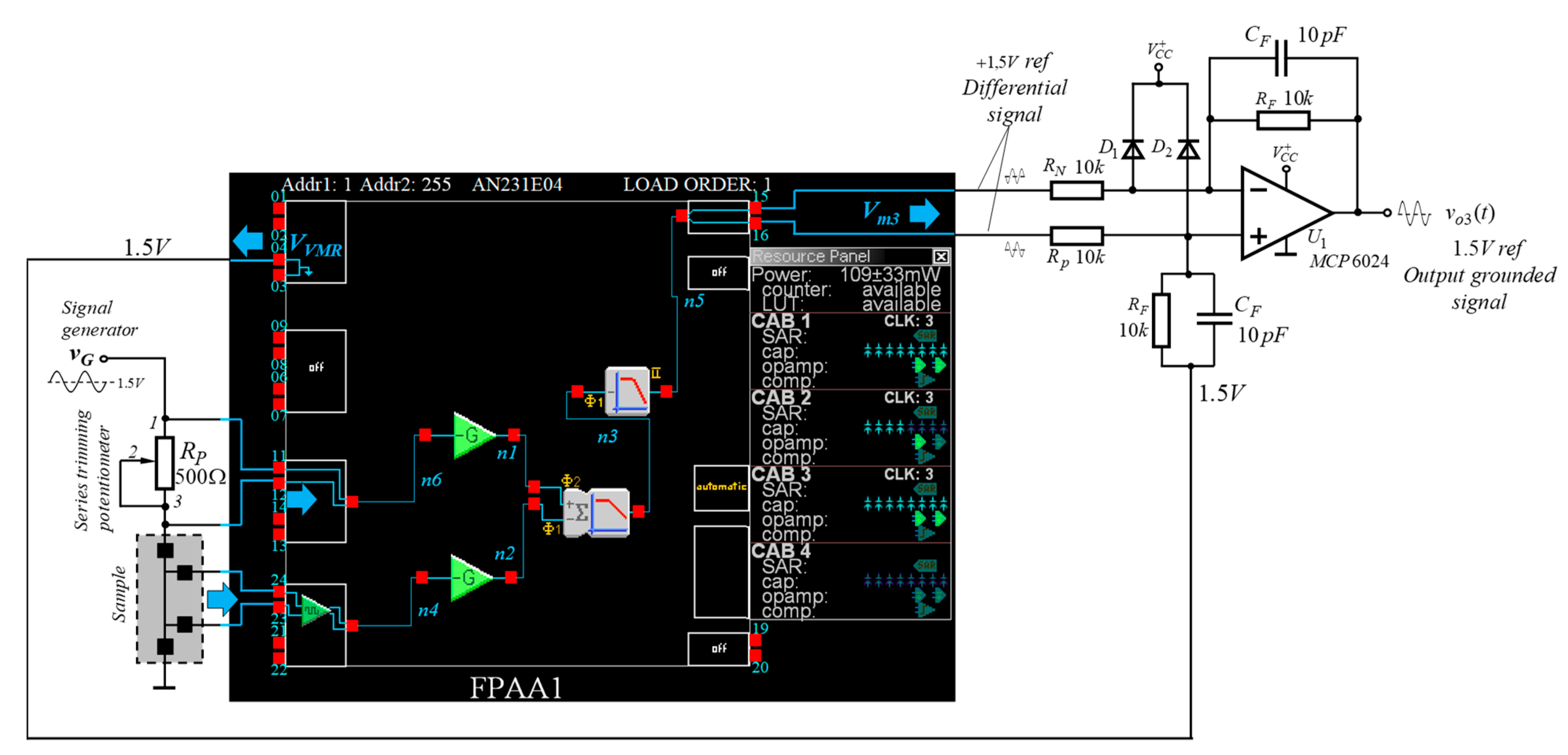
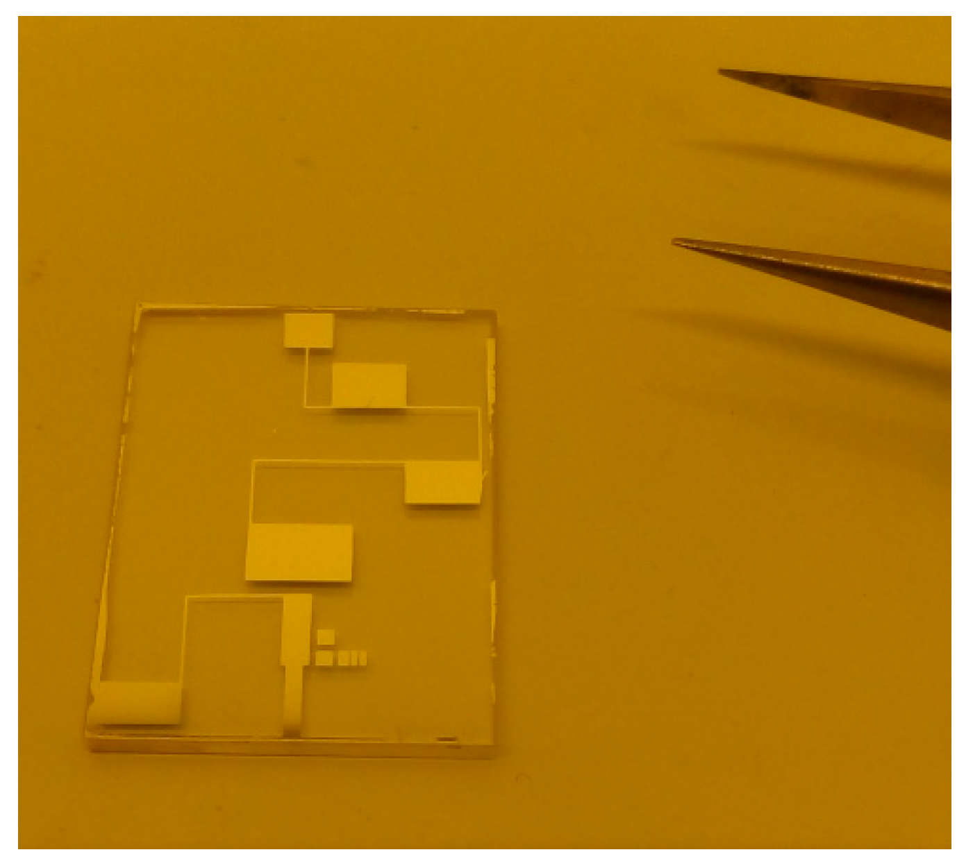
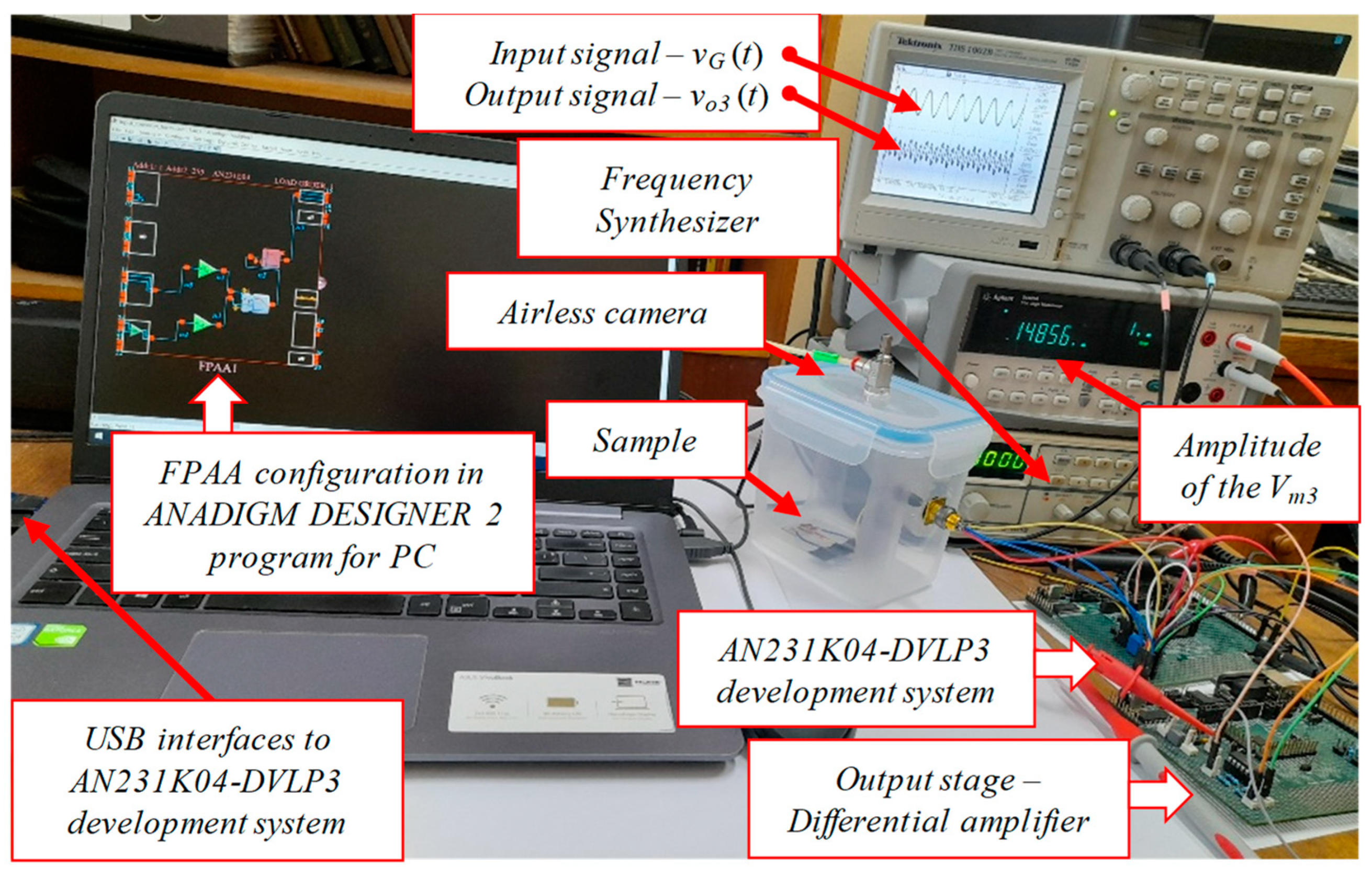
To demonstrate the workability of the proposed programmable analog circuit, various samples were studied to measure the thermal conductivity based on the method. The electronic circuit was implemented by using AN231K04-DVLP3 development system built around the FPAA AN231E04. The output difference amplifier was built on a separate PCB, but operating with the same single power supply voltage, equal to 3.3V. The experimental setup for the prototype of the programmable analog circuit integrated with the novel thin-film structure, serving as a proof of concept, is shown in Figure 5. Before examining the coefficient of thermal conductivity of the prepared samples, a reference sample of a silver thin film with known thermal characteristics, having a length of l = 7 mm, a resistance of R = 3.9 Ω and temperature coefficient of resistivity of 6.1×10
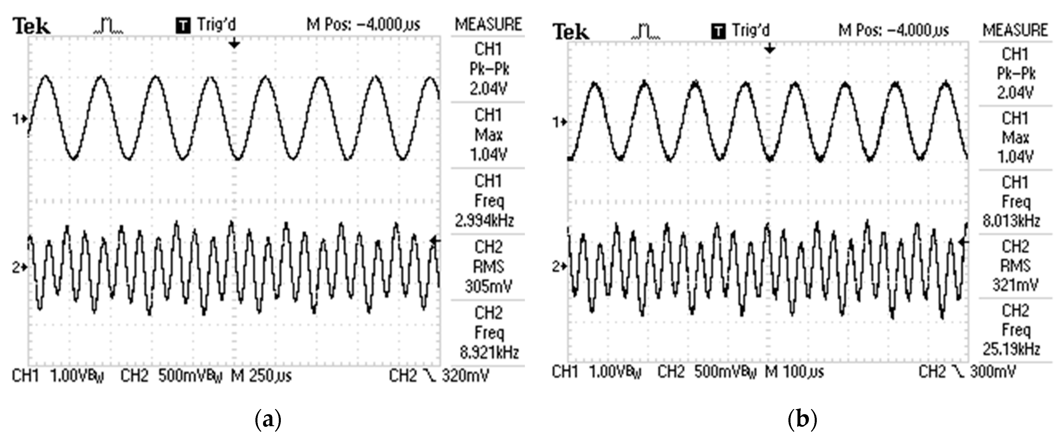
⁻³/°C was studied. In a similar way, similar to target perovskite films, the thin silver film was deposited on the sapphire substrate to ensure the lack of thermal conductivity to the substrate. The sample circuit with a thin silver film was placed in a vacuum chamber. In this case, two signals with frequencies of 3 kHz and 8 kHz, and an amplitude of 1 Vp-p was applied to the input voltage divider.
Figure 6a,b shows the oscillograms of the input and output signals. The effective values of the voltages were measured with a digital voltmeter and the difference was V o 3 r m s = V o 3 r m s , 1 V o 3 r m s , 2 = 265   mV 252   mV = 13   mV (where the quality factor of the output filter was chosen 50 (the value of the Q-factor can be up to 100, according the rms values of the output voltages)).
The value of the thermal conductivity coefficient was determined to be 459 W/mK (at 25 °C ambient temperature and 1 mbar pressure). The reference value of the thermal conductivity coefficient was approximately in the range from 406 (at 0 °C and 1 mbar) up to 419 W/mK (at 20 °C and 1 mbar) [25,26]. The relative error between the measured value with the proposed circuit and the approximate reference value is up to 15%, which guarantees a sufficient degree of accuracy in view of the tolerances of the technological parameters.
The iodine- and chlorine-based perovskite films, objects of investigation, were realized and tested under the same conditions as the thin silver film on a sapphire substrate. Both samples were with the same thickness and length and were also placed in a vacuum chamber. The measured coefficients of thermal conductivity for the iodine-based perovskite film was of 0.14W/mK at a temperature of 25 °C and pressure of 1 mbar ( V o 3 r m s = V o 3 r m s , 1 V o 3 r m s , 2 = 130   mV 118   mV = 12   mV , R = 300   k Ω and d R / d T = 40   k Ω / ° C ), and for the chlorine-based perovskite film it was of 0.084 W/mK at a temperature of 25 °C and pressure of 1 mbar ( V o 3 r m s = V o 3 r m s , 1 V o 3 r m s , 2 = 124   mV 104   mV = 20   mV , R = 300   k Ω and d R / d T = 40   k Ω / ° C ). The testing of both samples was performed under the same conditions and with the same frequencies of the input signals. The choice of other frequency pairs with a lower or higher value did not show significant differences in the above values for the coefficients. The differences from the measurement process with other frequency pairs showed a lower than 10%, which is acceptable.
The value of the thermal conductivity of the perovskite films are directly related to the stability of the solar cells, implementing these films, as it is a measure for the susceptibility of the material to be heated and to transfer heating to the neighboring layers. The sources of heat can be two types: (1) continuous illumination at maximal intensity of 1200 cd/m
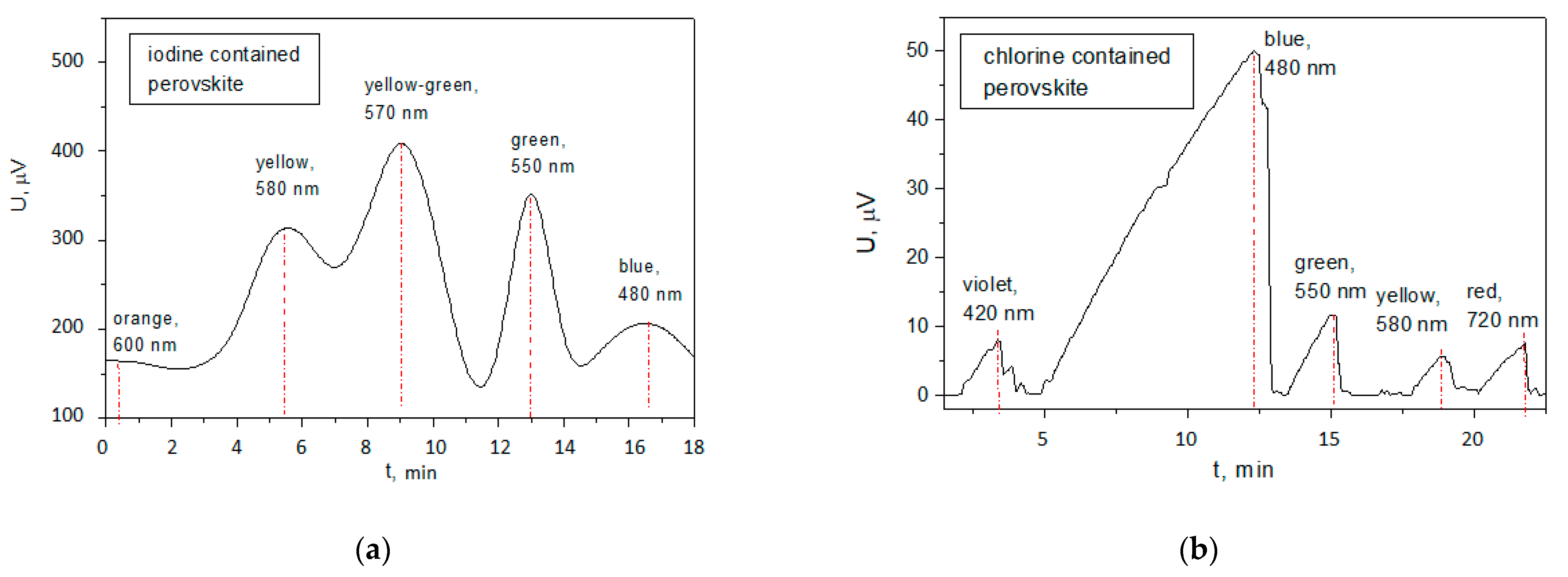
2 (according to the current standards) at a wavelength for which the material exhibited maximal spectral sensitivity and absorbed greater energy dose as compared to the rest wavelength components of the ultraviolet, visible and near infrared spectra; (2) direct heating due to the ambient temperature elevation. Therefore, for each of the two solar cells with the iodine- and chlorine-based perovskites, the spectral sensitivity characteristics were measured to find the wavelengths at which a maximum open circuit photovoltage was generated (Figure 7).
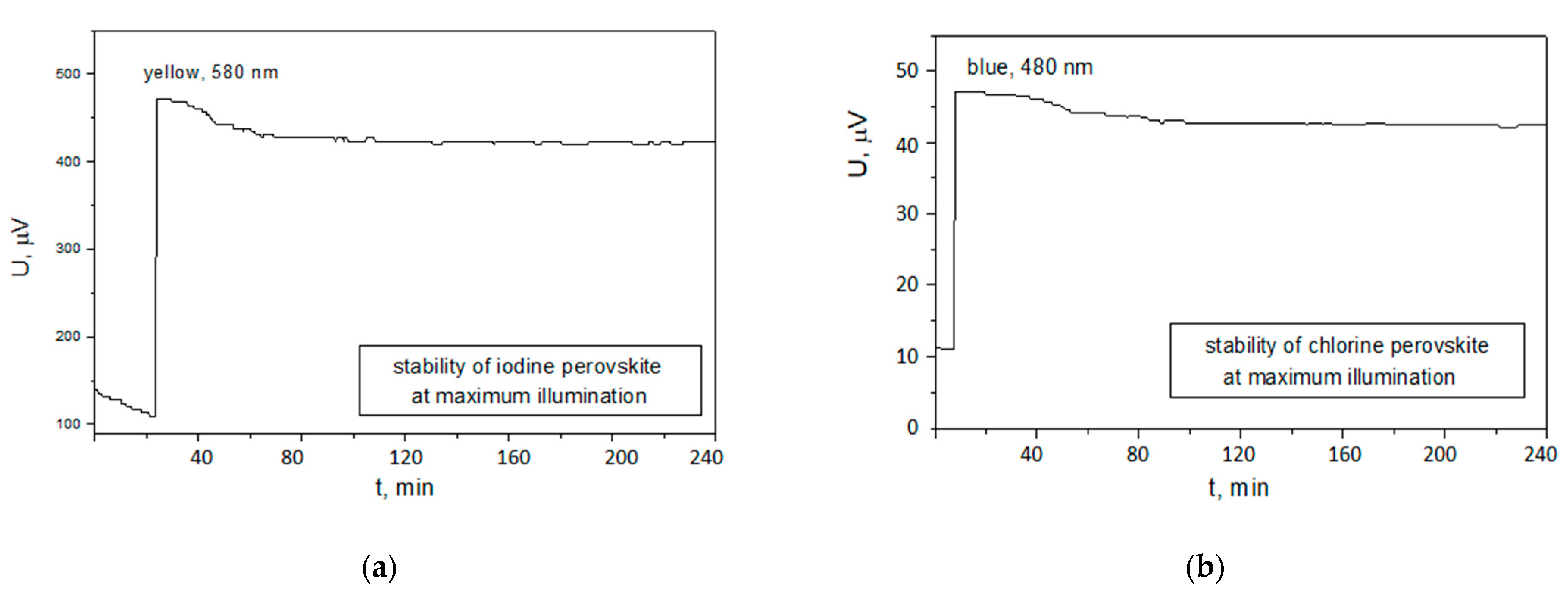
Iodine-based perovskite cell exhibited the highest photovoltage of 410 µV for a yellow-green light with a wavelength of 570 nm. For the chlorine-based perovskite, the maximum photovoltage was 49.6 µV at 480 nm (blue band). For this reason, a measurement was set for investigation of the stability of the open circuit photovoltage against time at continuous illumination with the light intensity and respective spectrum for which the corresponding cell exhibited the greatest photovoltage (Figure 8).
To eliminate the second source of heating that can affect the stability of the cell, this measurement was conducted at room temperature. The results showed an average rate of instability of 200 nV/min for the iodine-based perovskite cell and 20 nV/min for the chlorine-based perovskite cell (10 times slower). This trend of greater instability of the iodine-based device was expected considering its thermal conductivity, which was 1.6 times greater, as compared to the chlorine-based cell. Similar behavior of greater instability after the first hour of illumination can be noted for the two cells, afterward almost constant photovoltage was measured. Although additional studies are necessary to explore this effect in detail, it can be ascribed to the light-induced traps in the perovskite films. Once filled with the charge carriers they stop contributing for further photovoltage decrease [27]. After 4 h of continuous illumination, the photovoltage of the iodine-based perovskite solar cell dropped with 10.6% and the photovoltage of the chlorine-based cell—with 6.5%.
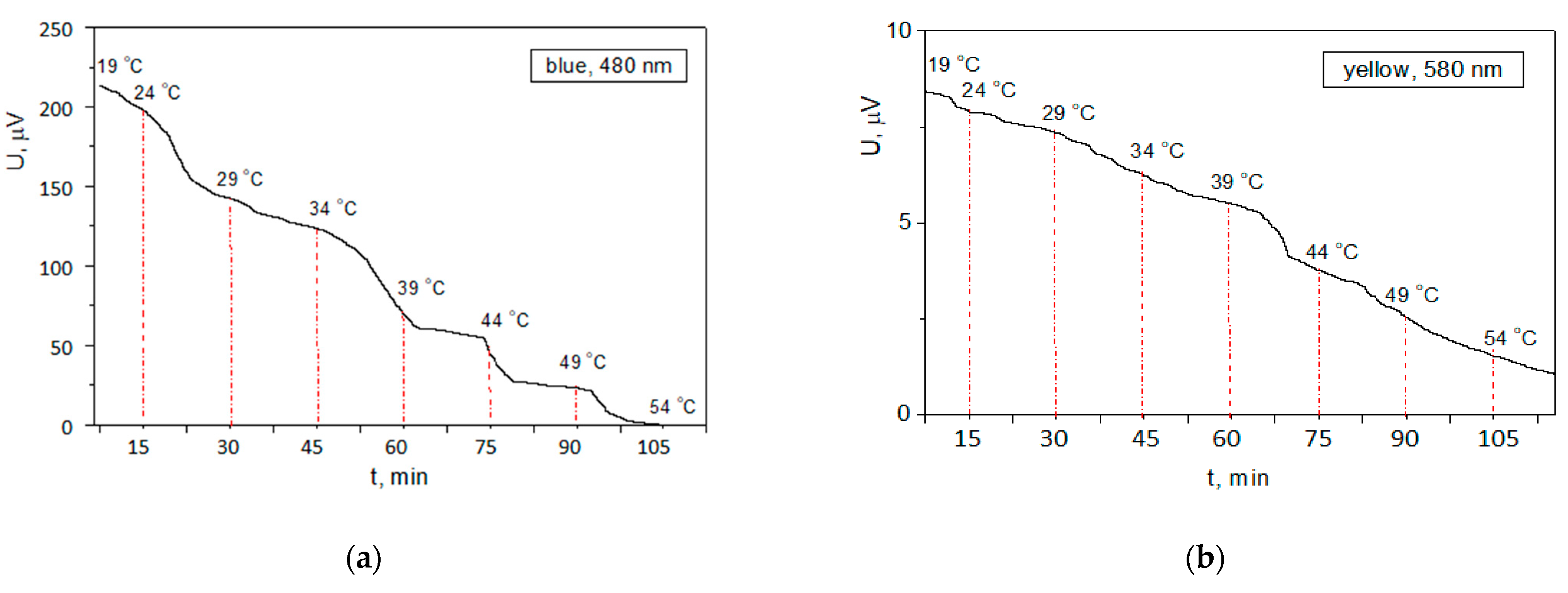
To study the effect of the ambient temperature variation on the stability of the two solar cells, the light exposure dose source of heat was elliminated to avoid its contribution to the deterioration of the electrical behavior of the cell. For this reason, the cells were illuminated with a light intensity of 500 cd/m2 and light spectrum falling in the opposite wavelength range against the spectrum component provoking maximum absorption sensitivity, i.e., blue illumination for the iodine-based cell and yellow for the chlorine- based. The temperature was increased at equal intervals of 15 min for establishing thermal equilibrium, considering the consisting materials and their thermal conductivity and capacity. The temperature change resolution was set to 5 °C as a compromise between the measurement rate and the accuracy of the temperature profile recording (Figure 9).
After 105 min, the photovoltage of the iodine-based cell dropped to zero, which is an indication of a complete thermal degradation of the perovskite molecules. The temperature greater than 49 °C probably resulted in chemical bond damages. Overall, the instability at this temperature variation was 15 µV/°C with a degradation rate of average 2.2 µV/min. For the same period, the photovoltage produced from the chlorine-based perovskite, although lower than its initial value, was still approximately a few microvolts, and can stand a temperature greater than 54 °C without complete thermal degradation of the molecules bonds. The instability at this temperature variation was 300 nV/°C with a degradation rate of 66 nV/min. This result is in excellent agreement with the obtained values for the thermal conductivity of the perovskite materials.
To summarize the devices’ performace, the main instability indicators together with the thermal conductivity for the studied materials were extracted in Table 2.

4. Conclusions

The method was successfully implemented by an FPAA-based programmable circuit for studying the thermal properties of new lead-free solar perovskite materials. The obtained signal contained valid information about the thermal conductivity of the measured samples and was validated by a reference sample. The precise determination of the thermal conductivity is a crucial factor for the relation with the device performance at heating conditions and for the correct interpretation of the stability data.
The novel iodine-based perovskite coating is characterized by a higher thermal conductivity. This results in a faster degradation of the photovoltage with the time at maximum illumination and greater variation of the photovoltage with the temperature as compared to the chlorine-based perovskite coating, showing lower thermal conductivity, and better stability, respectively.
The chlorine-based perovskite solar cell exhibited lower photovoltage, which is related to problems with the chemical synthesis and cannot be ascribed to thermal conductivity issues. After optimization of the synthesis procedure, promising behaviour in terms of greater stability with the time, illumination dose and temperature changes, in comparison with the iodine-based perovskite is expected.
Future work will be related to design and realize a suitable multiwire and multicontact topology for study of possible anisotropy in the thermal conductivity.

Author Contributions

Conceptualization, M.A. and I.P.; methodology, I.P.; software, I.P.; validation, M.A. and A.K.S.; formal analysis, M.A. and I.P.; investigation, M.A. and I.P.; resources, M.A. and A.K.S.; data curation, M.A.; writing—original draft preparation, M.A., I.P. and A.K.S.; writing—review and editing, M.A.; visualization, M.A. and I.P.; supervision, M.A.; project administration, M.A. and A.K.S.; funding acquisition, M.A. and A.K.S. All authors have read and agreed to the published version of the manuscript.

Funding

This study was funded by the Bulgarian National Science Fund, Grant No KP06-India-6/2019, BNSF, program Bulgaria-India scientific cooperation, competition 2018.

Data Availability Statement

The data presented in this study are available on request from the corresponding author.

Acknowledgments

This work was funded by an Indo-Bulgaria joint project, grant number KP06-Inida-6 of the Bulgarian National Science Fund. The authors are thankful to the colleagues from the academy of sciences for the materials provided and materials science issues consulting. The authors acknowledge the assistance of Georgi Kolev (Dept. of Microelectronics, TU-Sofia) for the vacuum measurement chamber design.

Conflicts of Interest

All authors declare that they have no conflict of interest.

Permission to Reproduce Material from Other Sources

Not applicable, as the paper contains own original results. They are presented on the 18th series of Advanced Energy Materials conference held at the Imperial College London from 6–8 April 2022.

References

  1. Deshpande, R.A. Advances in Solar Cell Technology: An Overview. J. Sci. Res. 2021, 65, 1–4. [Google Scholar] [CrossRef]
  2. Ehrmann, A.; Blachowicz, T. Recent coating materials for textile-based solar cells. AIMS Mater. Sci. 2019, 6, 234–251. [Google Scholar] [CrossRef]
  3. Jacak, J.E.; Jacak, W.A. Routes for Metallization of Perovskite Solar Cells. Materials 2022, 15, 2254. [Google Scholar] [CrossRef] [PubMed]
  4. Laska, M.; Krzemińska, Z.; Kluczyk-Korch, K.; Schaadt, D.; Popko, E.; Jacak, W.A.; Jacak, J.E. Metallization of solar cells, exciton channel of plasmon photovoltaic effect in perovskite cells. Nano Energy 2020, 75, 104751. [Google Scholar] [CrossRef]
  5. Wang, M.; Wang, W.; Ma, B.; Shen, W.; Liu, L.; Cao, K.; Chen, S. Lead-Free Perovskite Materials for Solar Cells. Nano-Micro Lett. 2021, 13, 62. [Google Scholar] [CrossRef] [PubMed]
  6. Tan, S.; Shi, J.; Yu, B.; Zhao, W.; Li, Y.; Li, Y.; Wu, H.; Luo, Y.; Li, D.; Meng, Q. Inorganic ammonium additive strategy for highly efficient and stable CsPbI3 perovskite solar cells. Adv. Funct. Mater. 2021, 31, 201081. [Google Scholar] [CrossRef]
  7. Girish, K.H.; Vishnumurthy, K.A.; Roopa, T.S. Role of conducting polymers in enhancing the stability and performance of perovskite solar cells: A brief review. Mater. Today Sustain. 2022, 17, 100090. [Google Scholar] [CrossRef]
  8. Jung, H.J.; Stompus, C.C.; Kanatzidis, M.G.; Dravid, V.P. Self-Passivation of 2D Ruddlesden-Popper Perovskite by Polytypic Surface PbI2 Encapsulation. Nano Lett. 2019, 19, 6109–6117. [Google Scholar] [CrossRef] [PubMed]
  9. Alidaei, M.; Ahmadi, V.; Mousavi, S.M.; Roghabadi, F.A. Stability improvement of perovskite solar cell using photoswitchable and moisture resistant dual-function interfacial layer. J. Alloy. Compd. 2022, 903, 163891. [Google Scholar] [CrossRef]
  10. Yusuf, A.O.; Orisekeh, K.; Oyelade, O.V.; Koech, R.K.; Ichwani, R.; Ebunu, A.I.; Amune, D.I.; Bello, A.; Anye, V.C.; Oyewole, O.K.; et al. Effects of temperature-dependent burn-in decay on the performance of triple cation mixed halide perovskite solar cells. AIP Adv. 2022, 12, 015122. [Google Scholar]
  11. Choi, K.; Lee, J.; Choi, H.; Kim, G.; Kim, H.I.; Park, T. Heat dissipation effects on the stability of planar perovskite solar cells. Sustain. Energy Fuels 2021, 5, 5523–5534. [Google Scholar] [CrossRef]
  12. David, G.C.; Pohl, R.O. Thermal conductivity of amorphous solids above the plateau. Phys. Rev. B 1987, 35, 4067–4073. [Google Scholar] [CrossRef]
  13. Kaul, P.B.; Day, K.A.; Abramson, A.R. Application of the three omega method for the thermal conductivity measurement of polyaniline. J. Appl. Phys. 2007, 101, 083507. [Google Scholar] [CrossRef]
  14. Yang, J.; Zhang, J.; Zhang, H.; Zhu, Y. Thermal conductivity measurement of thin films by a dc method. Rev. Sci. Instrum. 2010, 81, 114902. [Google Scholar] [CrossRef] [PubMed]
  15. Chernodoubov, D.A.; Inyushkin, A.V. Automatic thermal conductivity measurements with 3-omega technique. Rev. Sci. Instrum. 2019, 90, 024904. [Google Scholar] [CrossRef] [PubMed]
  16. Cretin, B. Scanning near-field thermal and thermoacoustic microscopy: Performances and limitations. Superlattices Microstruct. 2004, 35, 253–268. [Google Scholar] [CrossRef]
  17. Heiderhoff, R.; Haeger, T.; Pourdavoud, N.; Hu, T.; Al-Khafaji, M.; Mayer, A.; Chen, Y.; Scheer, H.; Riedl, T. Thermal Conductivity of Methylammonium Lead Halide Perovskite Single Crystals and Thin Films: A Comparative Study. J. Phys. Chem. C 2017, 121, 28306–28311. [Google Scholar] [CrossRef]
  18. Cahill, D.G. Thermal conductivity measurement from 30 to 750 K: The 3ω method. Rev. Sci. Instrum. 1990, 61, 802. [Google Scholar] [CrossRef]
  19. Jonsson, U.G.; Andersson, O. Investigations of the low- and high-frequency response of -sensors used in dynamic heat capacity measurements. Meas. Sci. Technol. 1998, 9, 1873. [Google Scholar] [CrossRef]
  20. Carslaw, H.; Jaeger, J. Conduction of Heat in Solids; Clarendon Press: Oxford, UK, 1959. [Google Scholar]
  21. AN231E04 Datasheet Rev. 1.5, 3rd Generation. Dynamically Reconfigurable dpASP, Anadigm USA, 2007. 2021. Available online: http://www.anadigm.com/_doc/DS231000-U001.pdf (accessed on 1 March 2022).
  22. Interfacing Analog Signals to the Anadigmvortex FPAA Devices; Application Note 205; Anadigm: Santa Clara, CA, USA, 2003.
  23. AN231K04-DVLP3–AnadigmApex Development Board. Available online: http://www.anadigm.com/_doc/UM231000-K001.pdf (accessed on 1 March 2022).
  24. Understanding AnadigmUnderstanding Anadigm® Configurable Analog Modules (CAMs), (November 2002), Anadigm, Mesa, AZ, 85203, USA. Available online: https://www.anadigm.com/_apps/PR021100-0024.pdf (accessed on 1 March 2022).
  25. Young, H.D. University Physics, 7th ed.; Addison Wesley: Boston, MA, USA, 1992. [Google Scholar]
  26. Carvill, J. Thermodynamics and Heat Transfer. In Mechanical Engineer’s Data Handbook; Elsevier: Amsterdam, The Netherlands, 1993; Volume 3, pp. 102–145. [Google Scholar]
  27. Dobrikov, G.H.; Aleksandrova, M.P.; Dobrikov, G.M. Thermally activated current for defect analysis in electroluminescent devices based on new synthesized low-molecular weight compound. In Proceedings of the 14th International workshop on Nanoscience and Nanotechnology, NANO2012, Sofia, Bulgaria, 22–23 November 2012; p. 89. [Google Scholar]
Figure 1. Schematic of the microstrip material of interest deposited on a thermal insulating substrate together with the connective contact pads, necessary for the 3ω measurements.
Crystals 12 01326 g001
Figure 2. Block diagram of the programmable analog circuit for measuring the amplitude of a third harmonic, which is generated in the study of thin-film solar cells.
Crystals 12 01326 g002
Figure 3. FPAA-based programmable circuit diagram used for thermal conductivity measurement, applying the method.
Crystals 12 01326 g003
Figure 4. Photo of the prepared sample with wire-shaped, four-contact pad perovskite film.
Crystals 12 01326 g004
Figure 5. Experimental setup for the prototype of the programmable analog circuit integrated with the novel thin-film structure.
Crystals 12 01326 g005
Figure 6. Input waveforms—CH1 and output waveforms—CH2 of the FPAA-based programmable analog circuit for the reference thin-film sample: (a) at input frequency equal to 3 kHz; (b) at input frequency equal to 8 kHz.
Crystals 12 01326 g006
Figure 7. Spectral sensitivity of the solar cell with: (a) iodine-based perovskite film; (b) chlorine-based perovskite film.
Crystals 12 01326 g007
Figure 8. Stability of the photovoltage against time at room temperature and at a maximum illumination with the specific absorption wavelength: (a) for the iodine-based perovskite solar cell; (b) for the chlorine-based perovskite solar cell.
Crystals 12 01326 g008
Figure 9. Stability of the photovoltage against temperature at a constant illumination: (a) for the iodine-based perovskite solar cell; (b) for the chlorine-based perovskite solar cell.
Crystals 12 01326 g009
Table 1. Cams for the proposed analog circuit according to the schematic in Figure 3.
NameSymbolOptionsParameters
IOCell1
(ANx3_iocell1 v1.2.1)
Crystals 12 01326 i001I/O Mode: Output port
Output Type: VMR ≈ 1.5V
none
IOCell4
(ANx3_iocell1a v1.2.1)
Crystals 12 01326 i002I/O Mode: Low offset input chopper amplifierGain: 0dB or Unity
IOCell5
(ANx3_iocell2 v1.0.1)
Crystals 12 01326 i003I/O Mode: Output port
Output Type: Bypass
none
GainInv1 and GainInv2
(GainInv v1.0.1)
Crystals 12 01326 i004noneGain: 1
Clock A: 250 kHz (Chip Clock 3)
SumFilter1
(SumFilter v1.0.2)
Crystals 12 01326 i005Output Changes On: Phase 1
Input 1: Non-inverting
Input 2: Inverting
Corner Frequency [kHz]:25.0
Gain 1 (Upper input port) 1.00
Gain 2 (Lower input port)1.00
Clock A: 250 kHz
FilterBiquad1
(FilterBiquad v1.0.2)
Crystals 12 01326 i006Filter Type: Low Pass
Input Sampling Phase: Phase 1
Polarity: Inverting configuration
Corner Frequency [kHz]: Fc_value
Gain: 1.00
Quality Factor: Q_value
Clock A: 250 kHz
Table 2. Performance of the solar cells, comparing different stability indicators.
Material Time Related Instability, nV/minThermal Conductivity, W/mKPhotovoltage
Drop, %
Temperature
Instability, µV/°C
Iodine perovskite2000.1410.615
Chlorine perovskite200.0846.50.3
Publisher’s Note: MDPI stays neutral with regard to jurisdictional claims in published maps and institutional affiliations.

