
Abnormal Shear Performance of Microscale Ball Grid Array Structure Cu/Sn–3.0Ag–0.5Cu/Cu Solder Joints with Increasing Current Density


Abstract
:1. Introduction
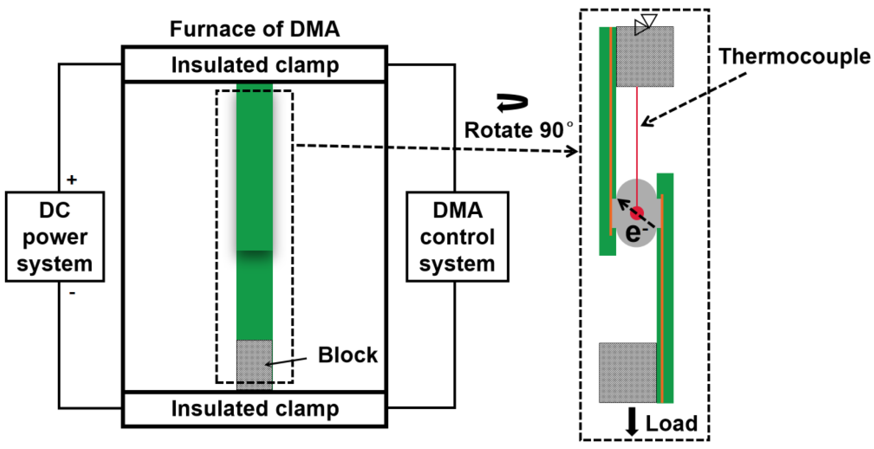
2. Experimental Procedure and Simulation Model
3. Results
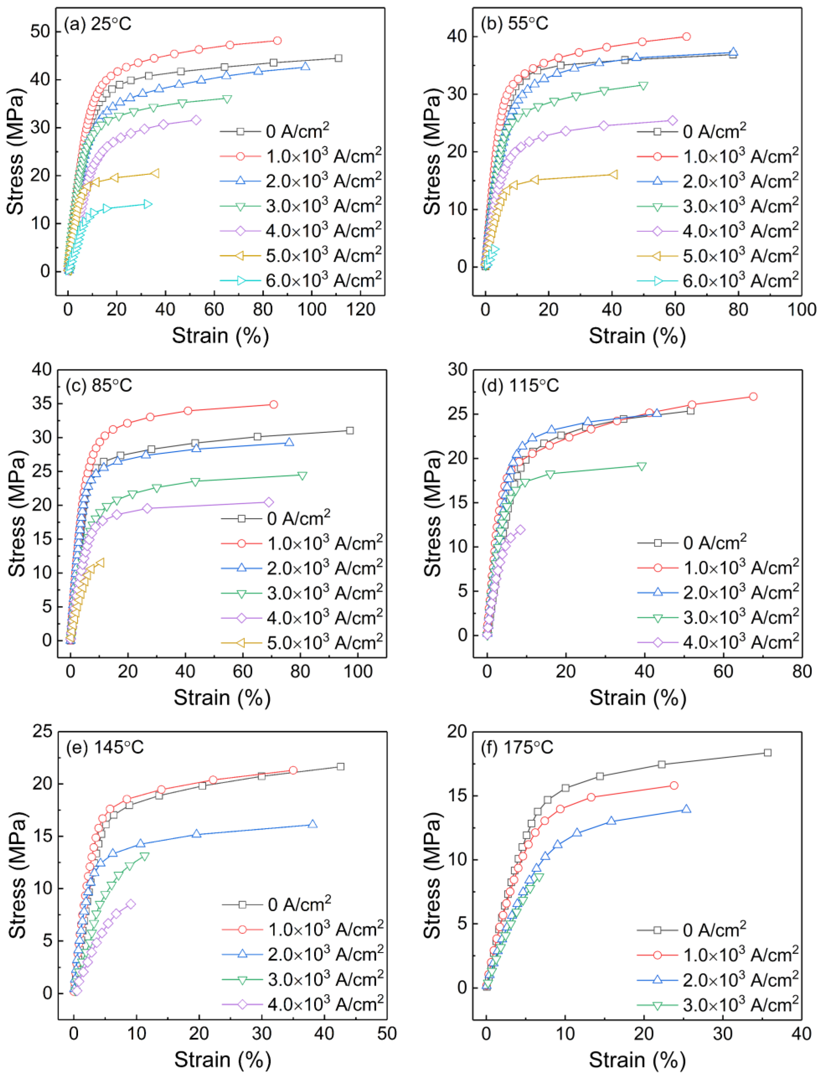
3.1. Deformation of Solder Joints under Current Stressing
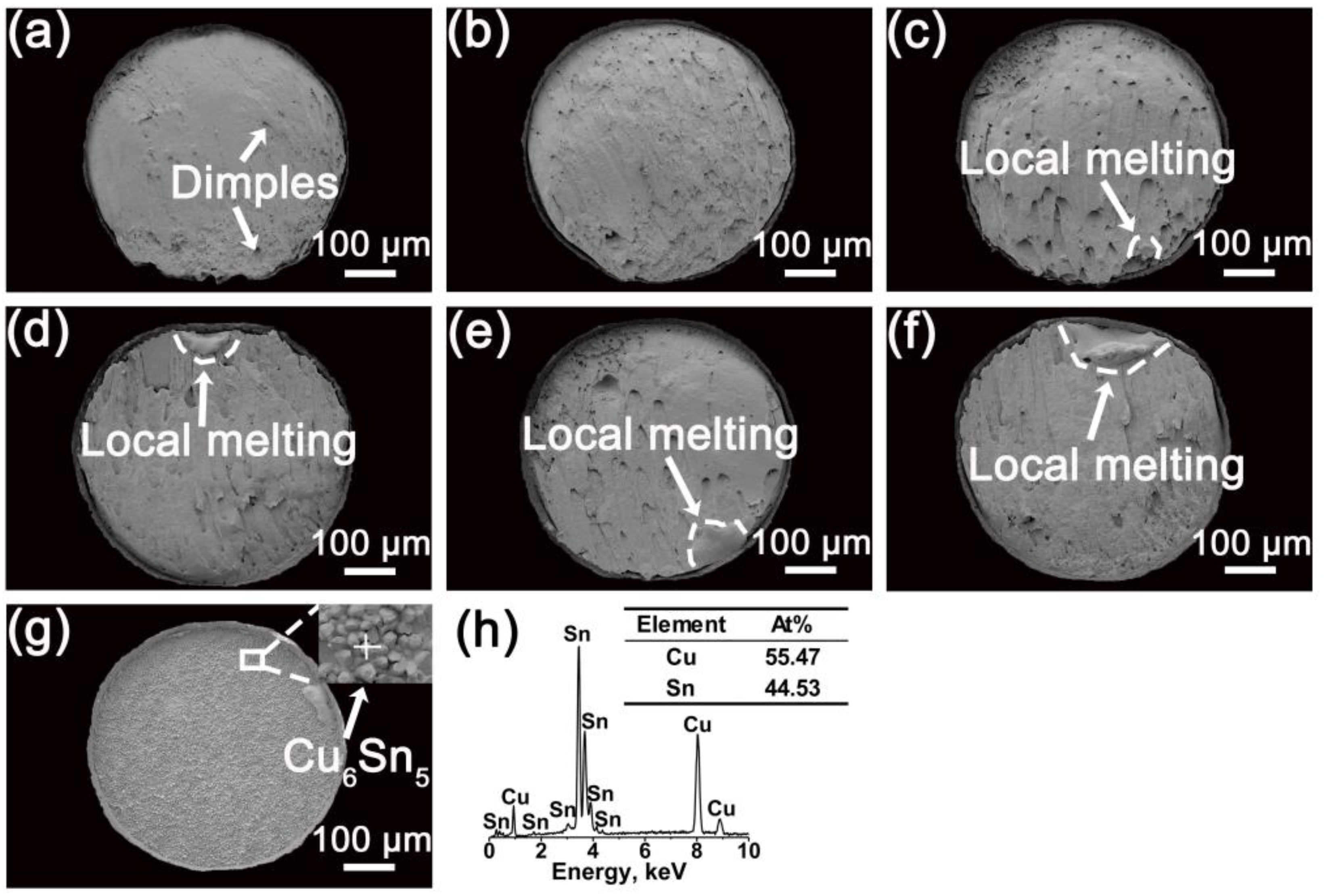
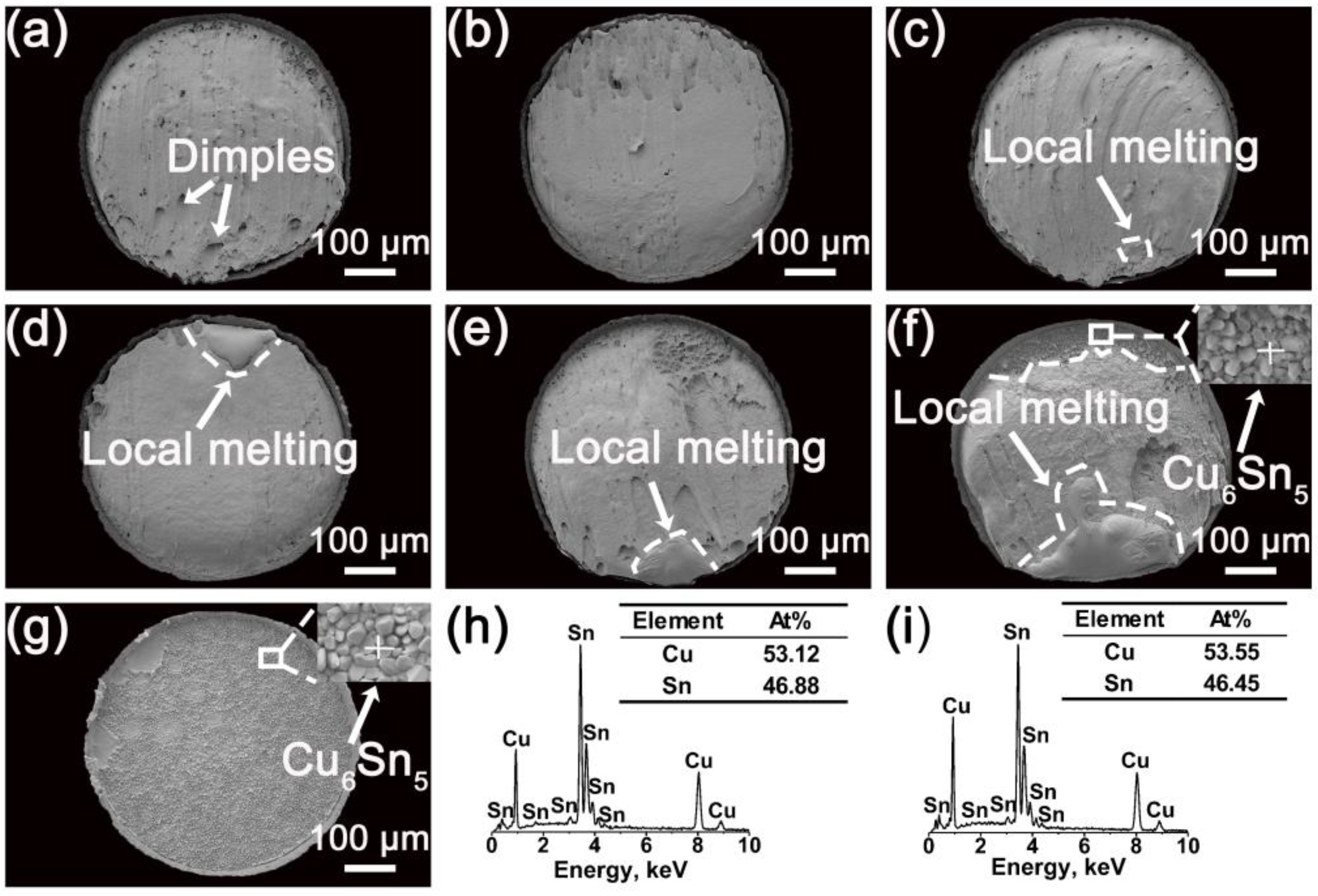
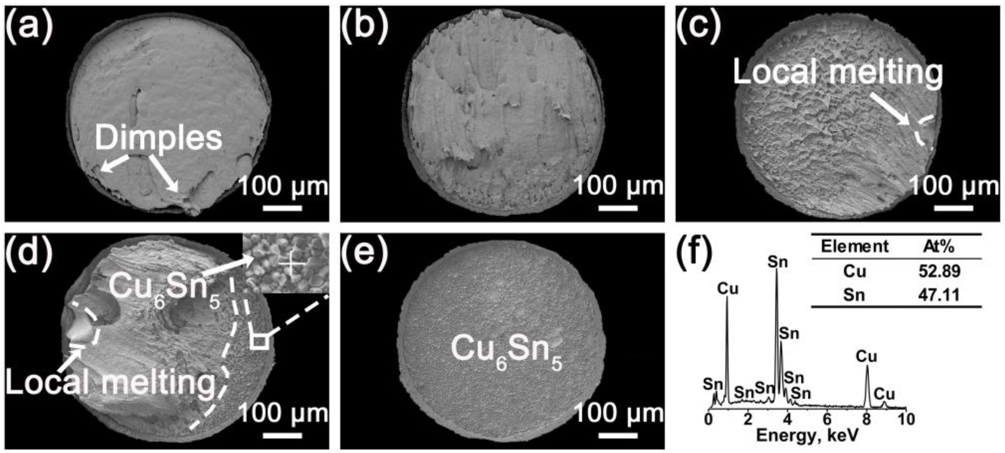
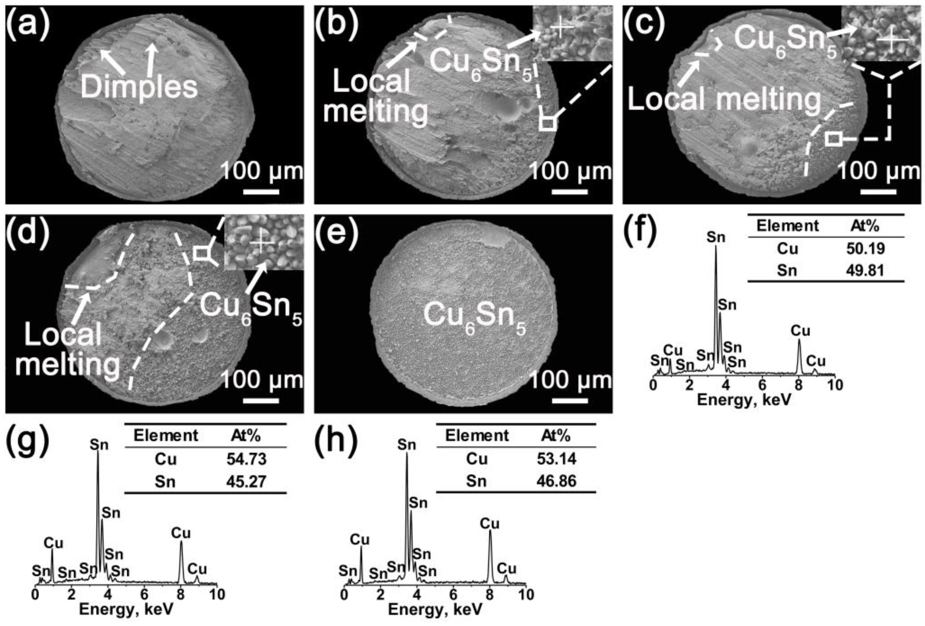
3.2. Fracture of Solder Joints under Current Stressing
4. Discussion
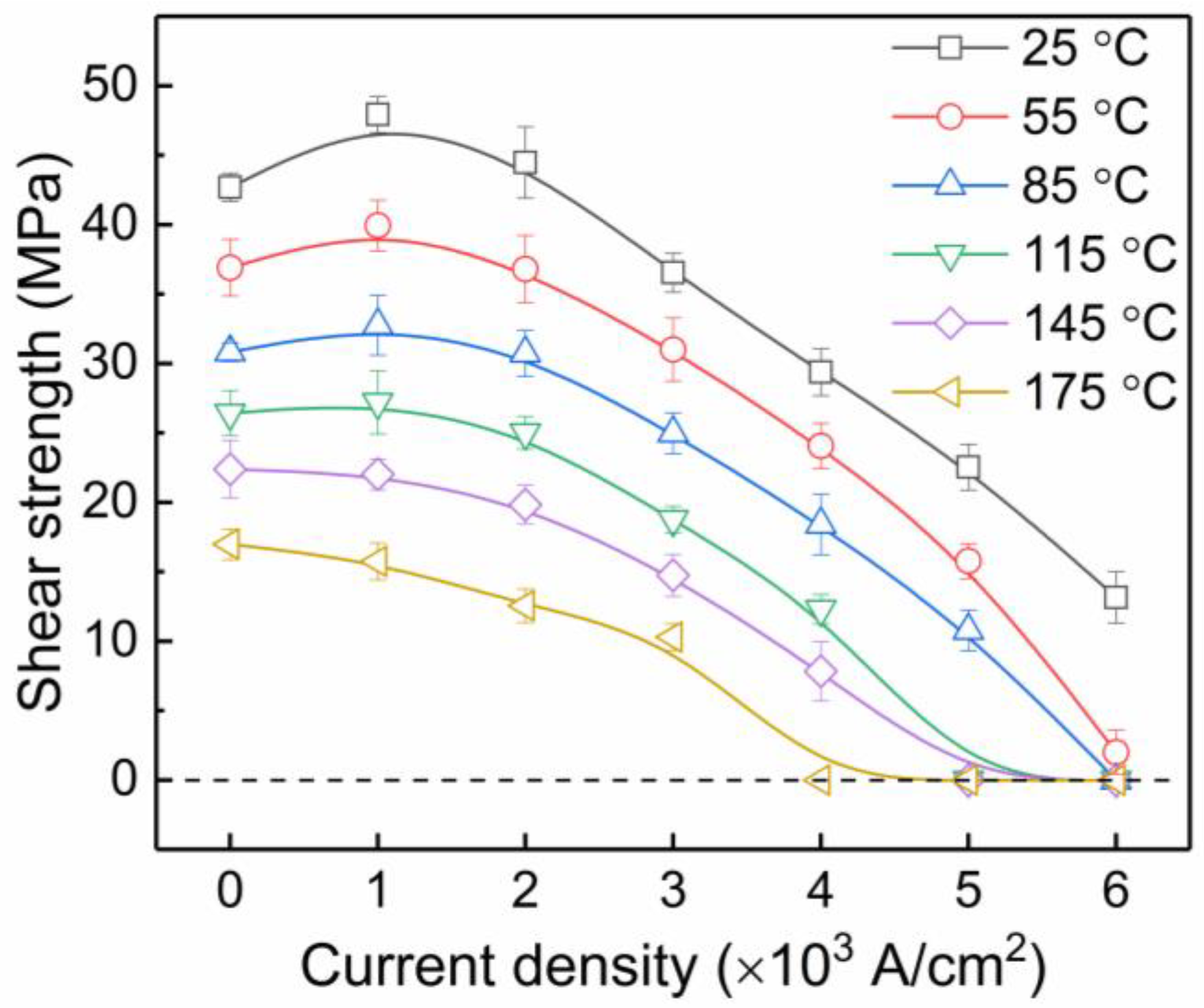
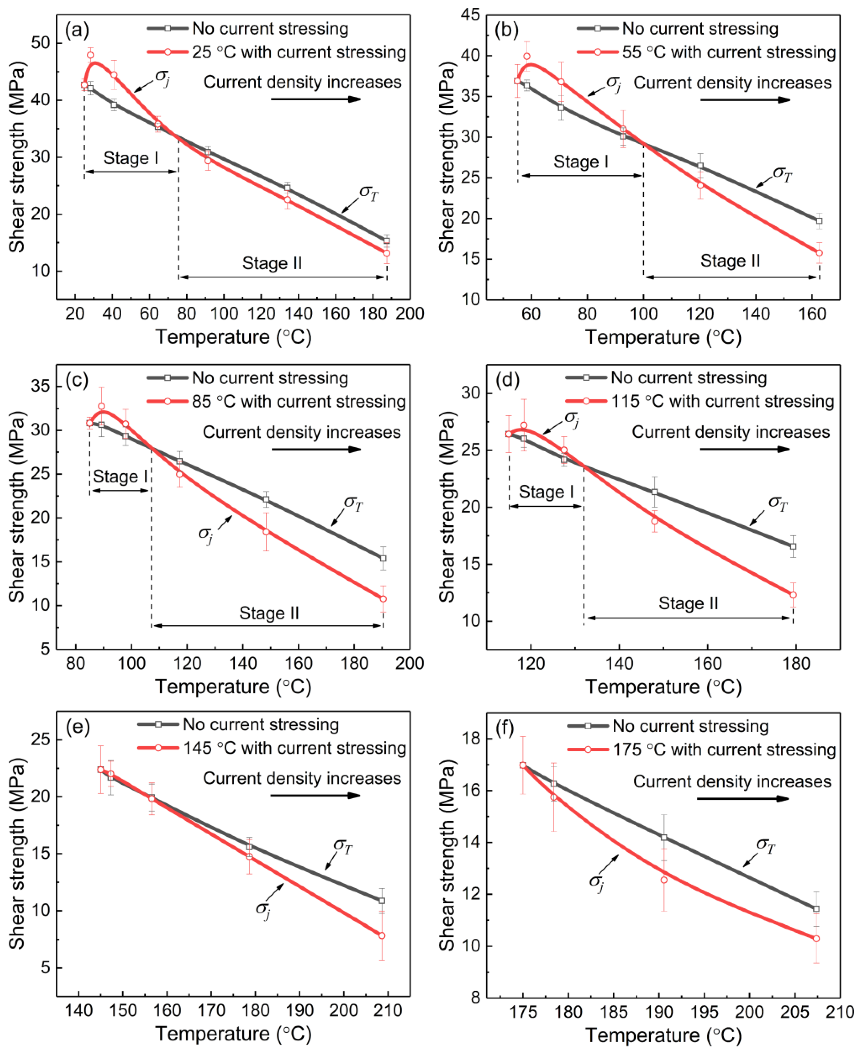
4.1. Shear Strength
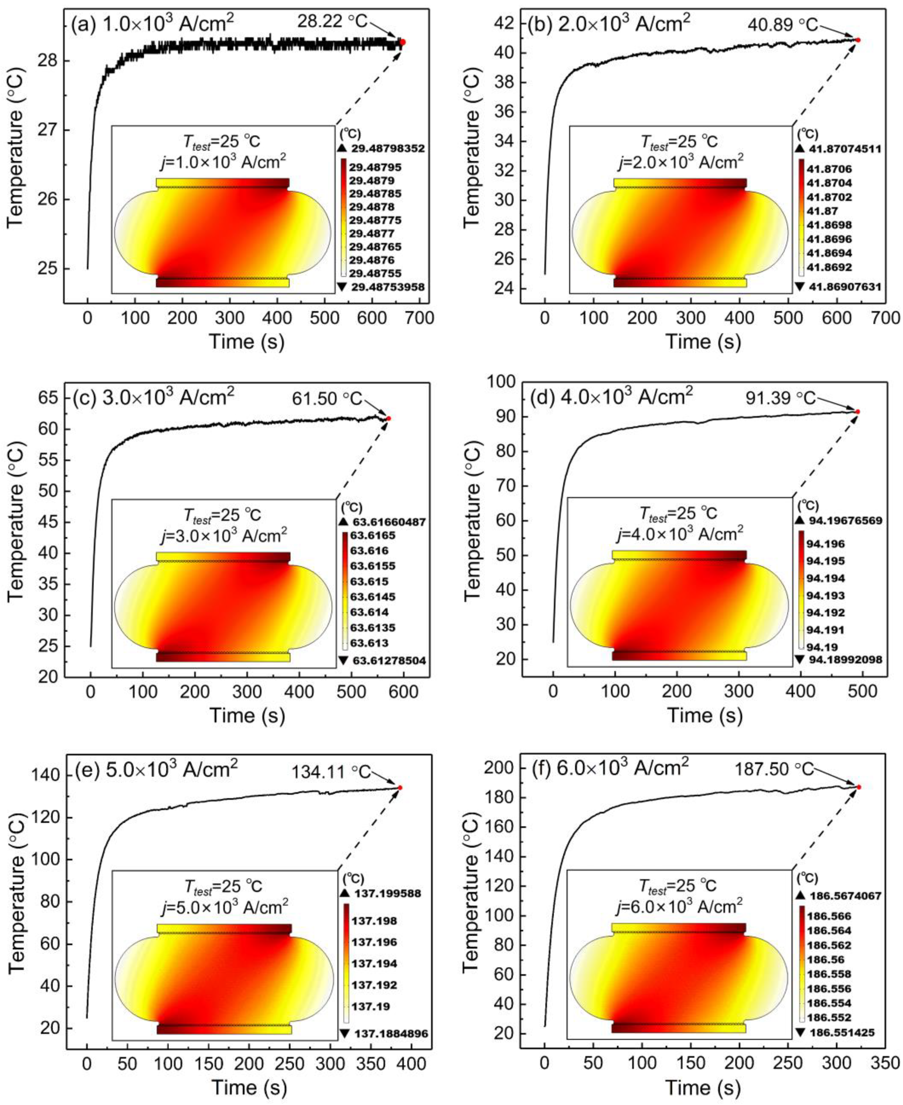
4.1.1. Influence of Joule Heating on the Shear Strength
4.1.2. Influence of Athermal Effect on Shear Strength
4.1.3. Influence of Current Stressing on Shear Strength
4.2. Fracture Behavior
5. Conclusions
- (1)
- The shear strength first increases then decreases with increasing current density at relatively low test temperatures (25–85 °C). The shear strength increase is weakened and gradually diminished as temperatures increase.
- (2)
- The abnormal variation of shear strength is induced by the counteraction of Joule heating and the athermal effect of current stressing. Joule heating dominates at the higher current densities and presents a deterioration state on the shear strength, while the contribution of the athermal effect of current stressing on shear strength changes from an enhancement state to a deterioration state with increasing current density, and the critical current density for this change decreases with increasing temperatures.
- (3)
- The fracture location of solder joints gradually shifts from the solder matrix to the solder/IMC layer interface, with increasing current density and showing an obvious ductile-to-brittle transition. The critical current density for this transition decreases with increasing temperatures.
Supplementary Materials
Author Contributions
Funding
Data Availability Statement
Conflicts of Interest
References
- Qin, H.B.; Li, W.Y.; Zhou, M.B.; Zhang, X.P. Low cycle fatigue performance of ball grid array structure Cu/Sn–3.0Ag–0.5Cu/Cu solder joints. Microelectron. Reliab. 2014, 54, 2911–2921. [Google Scholar] [CrossRef]
- Shnawah, D.A.; Said, S.B.M.; Sabri, M.F.M.; Badruddin, I.A.; Che, F.X. High-reliability low-Ag-content Sn–Ag–Cu solder joints for electronics applications. J. Electron. Mater. 2012, 41, 2631–2658. [Google Scholar] [CrossRef]
- Shu, C.C.; Liang, C.L.; Lin, K.L. Electro-work hardening of metals induced by the athermal electromigration effect. Mater. Sci. Eng. A 2020, 772, 138689. [Google Scholar] [CrossRef]
- Hu, X.W.; Xu, T.; Keer, L.M.; Li, Y.L.; Jiang, X.X. Microstructure evolution and shear fracture behavior of aged Sn3Ag0.5Cu/Cu solder joints. Mater. Sci. Eng. A 2016, 673, 167–177. [Google Scholar] [CrossRef]
- Kao, C.L.; Chen, T.C. Ball impact responses of Sn–1Ag–0.5Cu solder joints at different temperatures and surface finishes. Microelectron. Reliab. 2018, 82, 204–212. [Google Scholar] [CrossRef]
- Liu, Y.; Ren, B.Q.; Xue, Y.X.; Zhou, M.; Cao, R.X.; Chen, P.H.; Zeng, X.H. Microstructure and mechanical behavior of SnBi–xAg and SnBi–xAg@P–Cu solder joints during isothermal aging. Microelectron. Reliab. 2021, 127, 114388. [Google Scholar] [CrossRef]
- Ho, C.E.; Lee, P.T.; Chen, C.N.; Yang, C.H. Electromigration in 3D-IC scale Cu/Sn/Cu solder joints. J. Alloys Compd. 2016, 676, 361–368. [Google Scholar] [CrossRef]
- Zhang, P.; Xue, S.B.; Wang, J.H. New challenges of miniaturization of electronic devices: Electromigration and thermomigration in lead-free solder joints. Mater. Des. 2020, 192, 108726. [Google Scholar] [CrossRef]
- Geczy, A.; Straubinger, D.; Kovacs, A.; Krammer, O.; Mach, P.; Harsányi, G. Effects of high current density on lead-free solder joints of chip-size passive SMD components. Solder. Surf. Mt. Technol. 2018, 30, 74–80. [Google Scholar] [CrossRef]
- Straubinger, D.; Geczy, A.; Sipos, A.; Kiss, A.; Gyarmati, D.; Krammer, O.; Rigler, D. Advances on high current load effects on lead-free solder joints of SMD chip-size components and BGAs. Circuit World 2019, 45, 37–44. [Google Scholar] [CrossRef]
- Wang, X.J.; Zeng, Q.L.; Zhu, Q.S.; Wang, Z.G.; Shang, J.K. Effects of current stressing on shear properties of Sn–3.8Ag–0.7Cu solder joints. J. Mater. Sci. Technol. 2010, 26, 737–742. [Google Scholar] [CrossRef]
- Chang, H.; Li, M.Y. Influence of electromigration on the shear strength of Sn3.0Ag0.5Cu Pb-free solder joint. Electron. Compon. Mater. 2011, 30, 29–31. [Google Scholar]
- Lu, Y.D.; En, Y.F.; He, X.Q.; Niu, G.; Pecht, M.; Wang, X. Ductile-to-brittle transition of flip-chip solder joints influenced by electromigration. In Proceedings of the 2010 11th International Conference on Electronic Packaging Technology & High Density Packaging, Xi’an, China, 16–19 August 2010; pp. 824–827. [Google Scholar]
- Yang, L.; Ge, J.G.; Zhang, Y.C.; Dai, J.; Jing, Y.F. Electromigration reliability for Al2O3-reinforced Cu/Sn–58Bi/Cu composite solder joints. J. Mater. Sci. Mater. Electron. 2017, 28, 3004–3012. [Google Scholar] [CrossRef]
- Wang, X.J.; Li, T.Y.; Chen, Y.X.; Wang, J.X. Current induced interfacial microstructure and strength weakening of SAC/FeNi-Cu connection. Appl. Mech. Mater. 2014, 651, 11–15. [Google Scholar] [CrossRef]
- Hu, X.; Chan, Y.C.; Zhang, K.L.; Yung, K.C. Effect of graphene doping on microstructural and mechanical properties of Sn–8Zn–3Bi solder joints together with electromigration analysis. J. Alloys Compd. 2013, 580, 162–171. [Google Scholar] [CrossRef]
- Le, W.K.; Zhou, J.Y.; Ke, C.B.; Zhou, M.B.; Zhang, X.P. Study of accelerated shear creep behavior and fracture process of micro-scale ball grid array (BGA) structure Cu/Sn–3.0Ag–0.5Cu/Cu joints under coupled electro–thermo–mechanical loads. J. Mater. Sci. Mater. Electron. 2020, 31, 15575–15588. [Google Scholar] [CrossRef]
- Li, W.Y.; Jin, H.; Yue, W.; Tan, M.Y.; Zhang, X.P. Creep behavior of micro-scale Cu/Sn–3.0Ag–0.5Cu/Cu joints under electro-thermo-mechanical coupled loads. J. Mater. Sci. Mater. Electron. 2016, 27, 13022–13033. [Google Scholar] [CrossRef]
- Kinney, C.; Morris, J.W.; Lee, T.K.; Liu, K.C.; Xue, J.; Towne, D. The influence of an imposed current on the creep of Sn–Ag–Cu solder. J. Electron. Mater. 2009, 38, 221–226. [Google Scholar] [CrossRef]
- Jiao, Y.F.; Jermsittiparsert, K.; Krasnopevtsev, A.Y.; Yousif, Q.A.; Salmani, M. Interaction of thermal cycling and electric current on reliability of solder joints in different solder balls. Mater. Res. Express 2019, 6, 106302. [Google Scholar] [CrossRef]
- Zhu, Q.S.; Gao, F.; Ma, H.C.; Liu, Z.Q.; Guo, J.D.; Zhang, L. Failure behavior of flip chip solder joint under coupling condition of thermal cycling and electrical current. J. Mater. Sci. Mater. Electron. 2018, 29, 5025–5033. [Google Scholar] [CrossRef]
- Gao, F.; Zhu, Q.S.; Zheng, K.; Liu, Z.Q.; Guo, J.D.; Zhang, L.; Shang, J.K. Failure of chip sized packaging (CSP) under coupling fields of electrical current and thermal cycle. In Proceedings of the 2013 14th International Conference on Electronic Packaging Technology, Dalian, China, 11–14 August 2013; pp. 30–33. [Google Scholar]
- Li, W.Y.; Qin, H.B.; Zhou, M.B.; Zhang, X.P. Mechanical performance and fracture behavior of microscale Cu/Sn–3.0Ag–0.5Cu/Cu joints under electro-tensile coupled loads. J. Mech. Eng. 2016, 52, 46–53. [Google Scholar] [CrossRef]
- Li, W.Y.; Qin, H.B.; Zhou, M.B.; Zhang, X.P. The influence of imposed electric current on the tensile fracture behavior of micro-scale Cu/Sn–3.0Ag–0.5Cu/Cu solder joints. In Proceedings of the 2014 15th International Conference on Electronic Packaging Technology, Chengdu, China, 12–15 August 2014; pp. 1030–1034. [Google Scholar]
- Li, X.M.; Gui, J.; Li, W.Y.; Yan, H.D.; Qin, H.B.; Huang, J.Q.; Yang, D.G. Tensile performance of line–type microscale Cu/Sn–58Bi/Cu joints under electro-thermo-mechanical coupled loads. In Proceedings of the 2020 21st International Conference on Electronic Packaging Technology (ICEPT), Guangzhou, China, 12–15 August 2020; pp. 1–4. [Google Scholar]
- Le, W.K.; Ning, X.; Ke, C.B.; Zhou, M.B.; Zhang, X.P. Current density dependent shear performance and fracture behavior of micro-scale BGA structure Cu/Sn–3.0Ag–0.5Cu/Cu joints under coupled electromechanical loads. J. Mater. Sci. Mater. Electron. 2019, 30, 15184–15197. [Google Scholar] [CrossRef]
- Shen, J.; Cao, Z.M.; Zhai, D.J.; Zhao, M.L.; He, P.P. Effect of isothermal aging and low density current on intermetallic compound growth rate in lead-free solder interface. Microelectron. Reliab. 2014, 54, 252–258. [Google Scholar] [CrossRef]
- Fuller, S.; Sheikh, M.; Baty, G.; Kim, C.U.; Lee, T.K. Impact of in situ current stressing on Sn-based solder joint shear stability. J. Mater. Sci. Mater. Electron. 2021, 32, 2853–2864. [Google Scholar] [CrossRef]
- Gui, J.; Li, X.M.; Wang, J.; Li, W.Y.; Qin, H.B. Size effect on tensile performance of microscale Cu/Sn3.0Ag0.5Cu/Cu joints at low temperatures. J. Mater. Sci. Mater. Electron. 2021, 32, 28454–28467. [Google Scholar] [CrossRef]
- Smith, D.R.; Siewert, T.A.; Stephen, L.; Madeni, J.C. Database for Solder Properties with Emphasis on New Lead-Free Solders. In NIST Special Publications; 2002. Available online: www.nist.gov/publications/database-solder-properties-emphasis-new-lead-free-solders (accessed on 7 December 2021).
- An, T.; Qin, F.; Li, J.G. Mechanical behavior of solder joints under dynamic four-point impact bending. Microelectron. Reliab. 2011, 51, 1011–1019. [Google Scholar] [CrossRef]
- Huang, X.G.; Wang, Z.Q.; Yu, Y.Q. Thermomechanical properties and fatigue life evaluation of SnAgCu solder joints for microelectronic power module application. J. Mater. Res. Technol. 2020, 9, 5533–5541. [Google Scholar] [CrossRef]
- Kim, K.S.; Huh, S.H.; Suganuma, K. Effects of fourth alloying additive on microstructures and tensile properties of Sn–Ag–Cu alloy and joints with Cu. Microelectron. Reliab. 2003, 43, 259–267. [Google Scholar] [CrossRef]
- Tian, R.Y.; Hang, C.J.; Tian, Y.H.; Feng, J.Y. Brittle fracture induced by phase transformation of Ni–Cu–Sn intermetallic compounds in Sn–3Ag–0.5Cu/Ni solder joints under extreme temperature environment. J. Alloys Compd. 2019, 777, 463–471. [Google Scholar] [CrossRef]
- Nabarro, F.R.N. Dislocations in a simple cubic lattice. Proc. Phys. Soc. 1947, 59, 256–272. [Google Scholar] [CrossRef]
- Celli, V.; Kabler, M.; Ninomiya, T.; Thomson, R. Theory of dislocation mobility in semiconductors. Phys. Rev. 1963, 131, 58–72. [Google Scholar] [CrossRef]
- Li, W.G.; Yang, F.; Fang, D.N. The temperature-dependent fracture strength model for ultra–high temperature ceramics. Acta Mech. Sin. 2010, 26, 235–239. [Google Scholar] [CrossRef]
- Tang, W.B.; Long, X.; Yang, F.Q. Tensile deformation and microstructures of Sn–3.0Ag–0.5Cu solder joints: Effect of annealing temperature. Microelectron. Reliab. 2020, 104, 113555. [Google Scholar] [CrossRef]
- He, J.Y.; Lin, K.L.; Wu, A.T. The diminishing of crystal structure of Sn9Zn alloy due to electrical current stressing. J. Alloys Compd. 2015, 619, 372–377. [Google Scholar] [CrossRef]
- Chen, S.W.; Chen, C.M.; Liu, W.C. Electric current effects upon the Sn\Cu and Sn\Ni interfacial reactions. J. Electron. Mater. 1998, 27, 1193–1199. [Google Scholar] [CrossRef]
- Xu, L.H.; Pang, J.H.L.; Tu, K.N. Effect of electromigration-induced back stress gradient on nanoindentation marker movement in SnAgCu solder joints. Appl. Phys. Lett. 2006, 89, 221909. [Google Scholar] [CrossRef]
- Chao, B.; Chae, S.H.; Zhang, X.F.; Lu, K.H.; Im, J.; Ho, P.S. Investigation of diffusion and electromigration parameters for Cu–Sn intermetallic compounds in Pb-free solders using simulated annealing. Acta Mater. 2007, 55, 2805–2814. [Google Scholar] [CrossRef]
- Huang, H.C.; Lin, K.L.; Wu, A.T. Disruption of crystalline structure of Sn3.5Ag induced by electric current. J. Appl. Phys. 2016, 119, 115102. [Google Scholar] [CrossRef]
- Taylor, G.I. The mechanism of plastic deformation of crystals. Part, I. theoretical. Proc. R. Soc. A 1934, 145, 362–387. [Google Scholar]
- Poole, W.J.; Ashby, M.F.; Fleck, N.A. Micro-hardness of annealed and work–hardened copper polycrystals. Scr. Mater. 1996, 34, 559–564. [Google Scholar] [CrossRef]
- Zhang, P.; Li, S.X.; Zhang, Z.F. General relationship between strength and hardness. Mater. Sci. Eng. A 2011, 529, 62–73. [Google Scholar] [CrossRef]
- Suo, Z. Electromigration–induced dislocation climb and multiplication in conducting lines. Acta Metall. Mater. 1994, 42, 3581–3588. [Google Scholar] [CrossRef]
- Sprecher, A.F.; Mannan, S.L.; Conrad, H. Overview no. 49: On the mechanisms for the electroplastic effect in metals. Acta Metall. 1986, 34, 1145–1162. [Google Scholar] [CrossRef]
- Liu, Z.Y.; Liu, B.; Deng, X.T.; Lei, Y.; Cui, J.Z.; Bai, G.R. Effect of current pulse on mechanism of superplastic deformation of 2091 Al–Li alloy. Acta Metall. Sin. 2000, 36, 944–951. [Google Scholar]
- McQueen, H.J.; Blum, W. Dynamic recovery: Sufficient mechanism in the hot deformation of Al (<99.99). Mater. Sci. Eng. A 2000, 290, 95–107. [Google Scholar] [CrossRef]
- Verdier, M.; Brechet, Y.; Guyot, P. Recovery of AlMg alloys: Flow stress and strain–hardening properties. Acta Mater. 1999, 47, 127–134. [Google Scholar] [CrossRef]
- Mavrikakis, N.; Detlefs, C.; Cook, P.K.; Kutsal, M.; Campos AP, C.; Gauvin, M.; Calvillo, P.R.; Saikaly, W.; Hubert, R.; Poulsen, H.F.; et al. A multi-scale study of the interaction of Sn solutes with dislocations during static recovery in α–Fe. Acta Mater. 2019, 174, 92–104. [Google Scholar] [CrossRef]
- Li, W.Y.; Zhang, X.P.; Qin, H.B.; Mai, Y.W. Joule heating dominated fracture behavior change in micro-scale Cu/Sn–3.0Ag–0.5Cu/Cu(Ni) joints under electro-thermal coupled loads. Microelectron. Reliab. 2018, 82, 224–227. [Google Scholar] [CrossRef]


| Properties | SAC305 | Cu | Cu6Sn5 | FR4 |
|---|---|---|---|---|
| Electrical conductivity (107 S/m) | 0.87 [26] | 6.00 [26] | 0.57 [26] | 4.00 × 10⁻¹⁰ [26] |
| Thermal conductivity (W/(m·K)) | 57.3 [26] | 398.0 [30] | 34.1 [26] | 0.3 [26] |
| Density (g/cm3) | 7.38 [31] | 8.94 [31] | 8.28 [30] | 1.90 [26] |
| Young’s modulus (GPa) | 45.6 [32] | 117.0 [30] | 85.6 [30] | 22.0 [26] |
| Poisson’s ratio | 0.36 [31] | 0.35 [26] | 0.31 [26] | 0.15 [26] |
| CTE (10−6/k) | 21.2 [30] | 17.1 [30] | 16.3 [30] | 18.0 [26] |
| Specific heat capacity (J/(kg·K)) | 222.1 [30] | 385.2 [30] | 286.0 [30] | 1369.0 [26] |
Publisher’s Note: MDPI stays neutral with regard to jurisdictional claims in published maps and institutional affiliations. |
© 2022 by the authors. Licensee MDPI, Basel, Switzerland. This article is an open access article distributed under the terms and conditions of the Creative Commons Attribution (CC BY) license (https://creativecommons.org/licenses/by/4.0/).
Share and Cite
Wang, B.; Li, W.; Pan, K. Abnormal Shear Performance of Microscale Ball Grid Array Structure Cu/Sn–3.0Ag–0.5Cu/Cu Solder Joints with Increasing Current Density. Crystals 2022, 12, 85. https://doi.org/10.3390/cryst12010085
Wang B, Li W, Pan K. Abnormal Shear Performance of Microscale Ball Grid Array Structure Cu/Sn–3.0Ag–0.5Cu/Cu Solder Joints with Increasing Current Density. Crystals. 2022; 12(1):85. https://doi.org/10.3390/cryst12010085
Chicago/Turabian StyleWang, Bo, Wangyun Li, and Kailin Pan. 2022. "Abnormal Shear Performance of Microscale Ball Grid Array Structure Cu/Sn–3.0Ag–0.5Cu/Cu Solder Joints with Increasing Current Density" Crystals 12, no. 1: 85. https://doi.org/10.3390/cryst12010085
APA StyleWang, B., Li, W., & Pan, K. (2022). Abnormal Shear Performance of Microscale Ball Grid Array Structure Cu/Sn–3.0Ag–0.5Cu/Cu Solder Joints with Increasing Current Density. Crystals, 12(1), 85. https://doi.org/10.3390/cryst12010085