
The Design and Optimization of an Anti-Reflection Coating and an Intermediate Reflective Layer to Enhance Tandem Solar Cell Photons Capture


Abstract
:1. Introduction
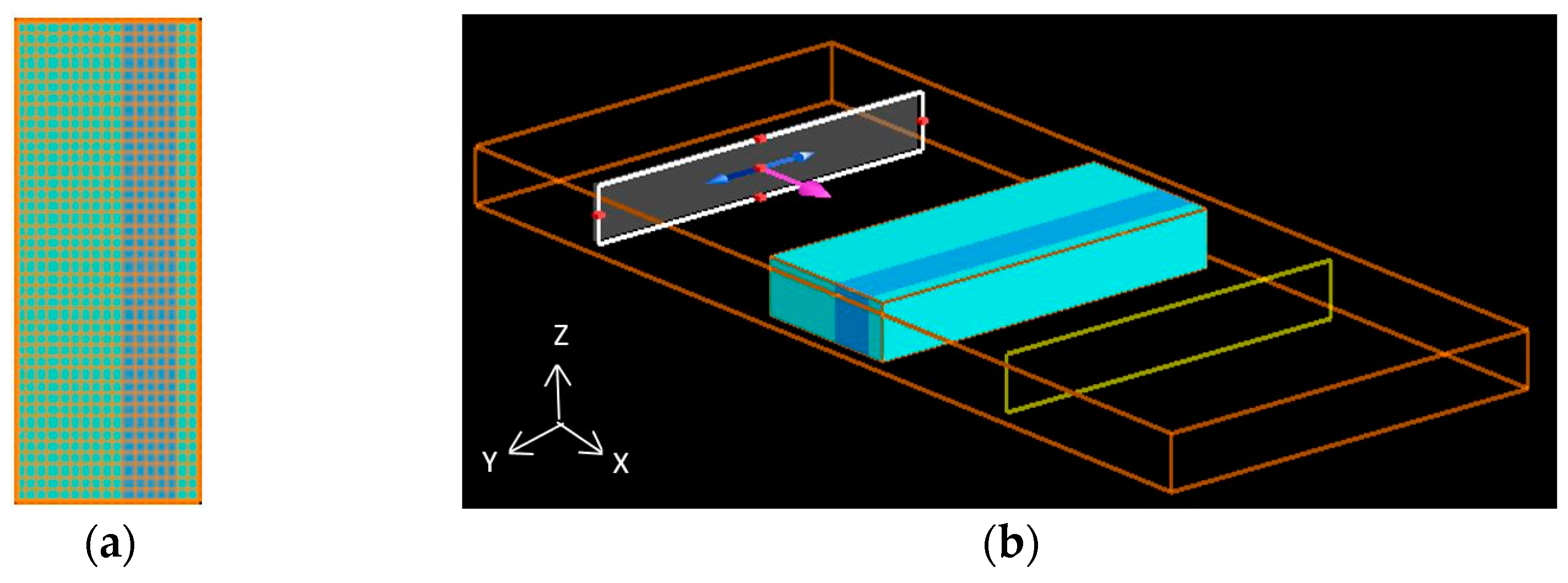
2. Modeling
2.1. Anti Reflection Coating (ARC)
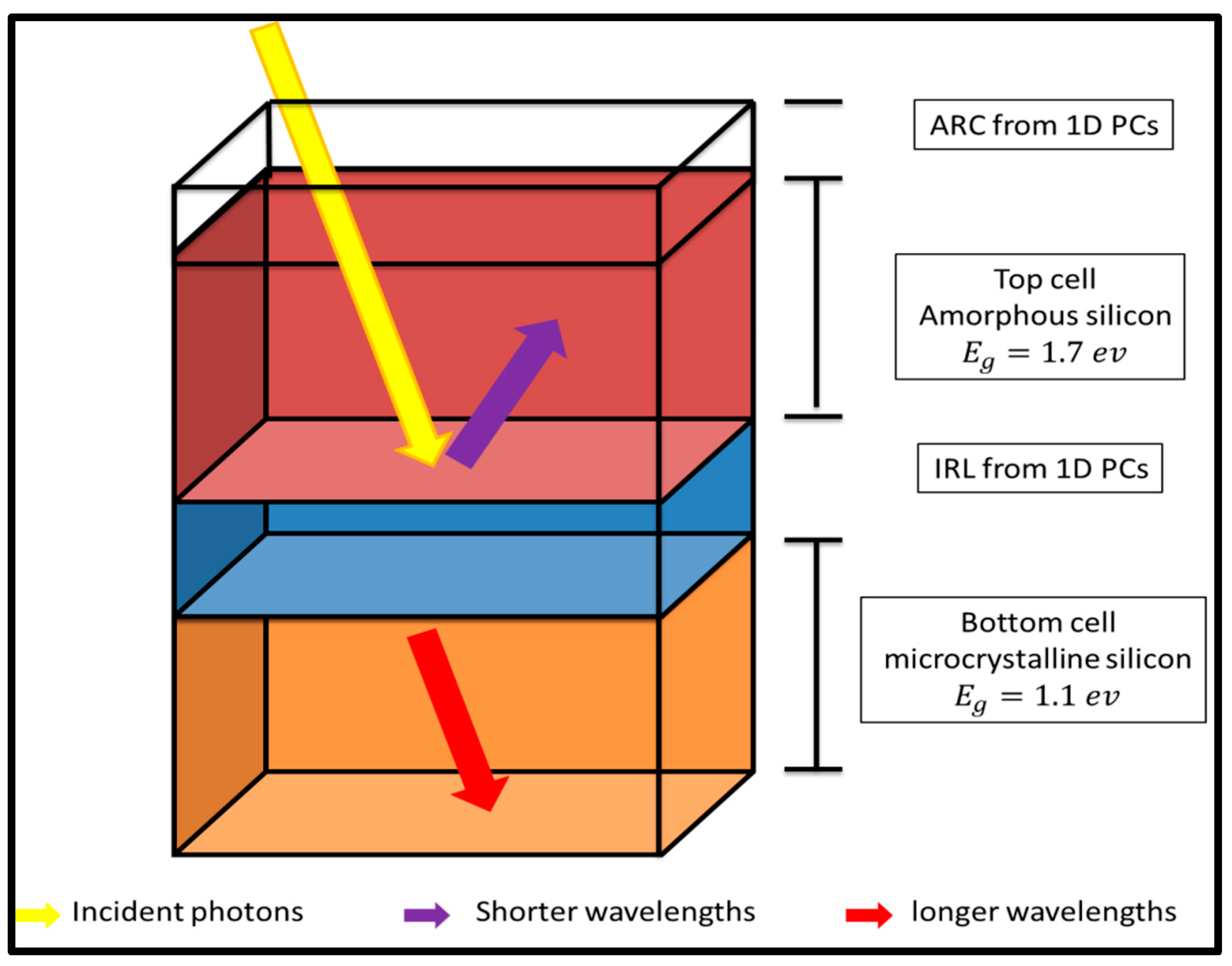
2.2. Intermediate Reflective Layer (IRL)
3. Result and Discussion
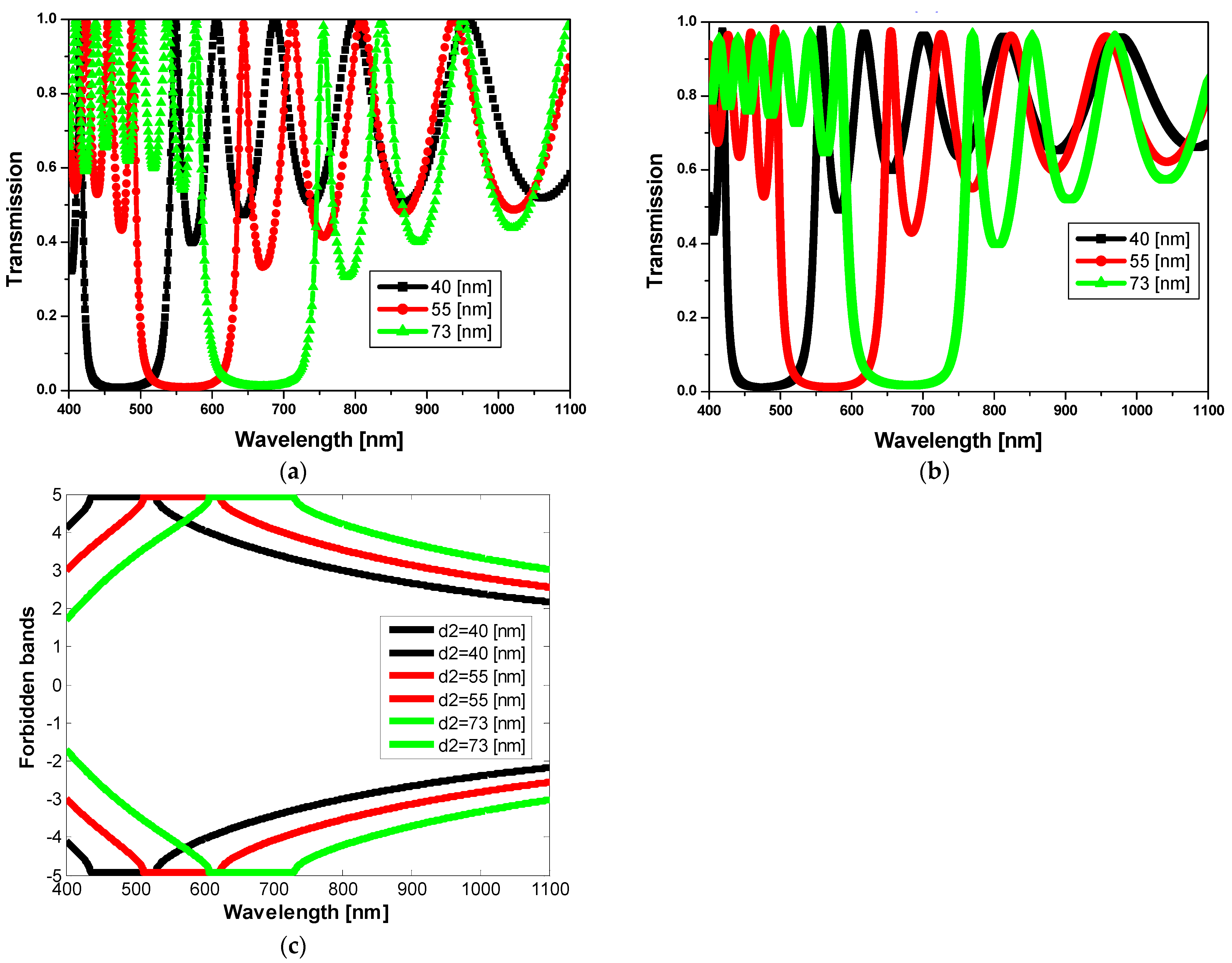
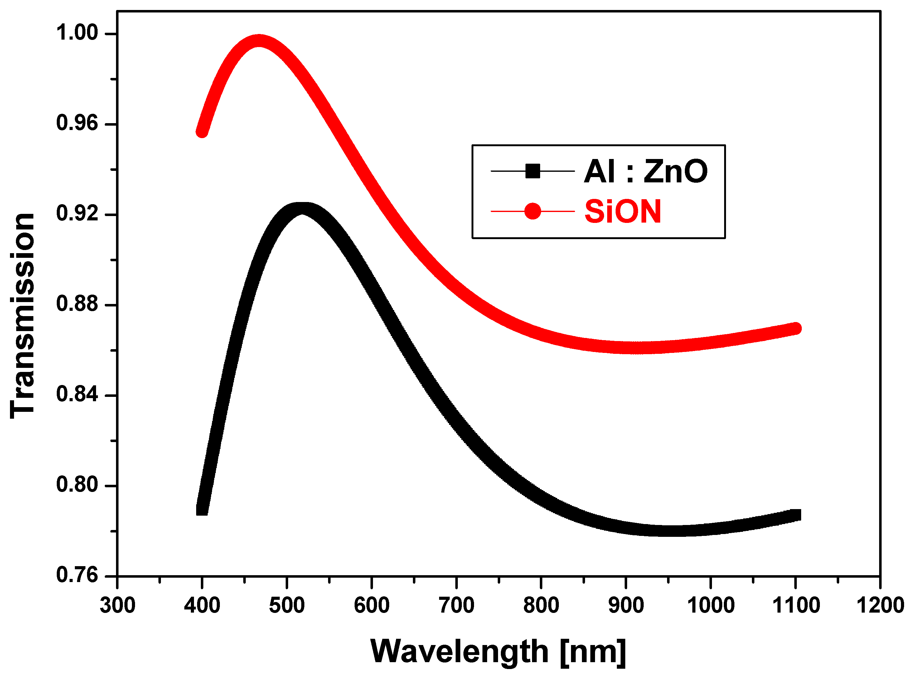
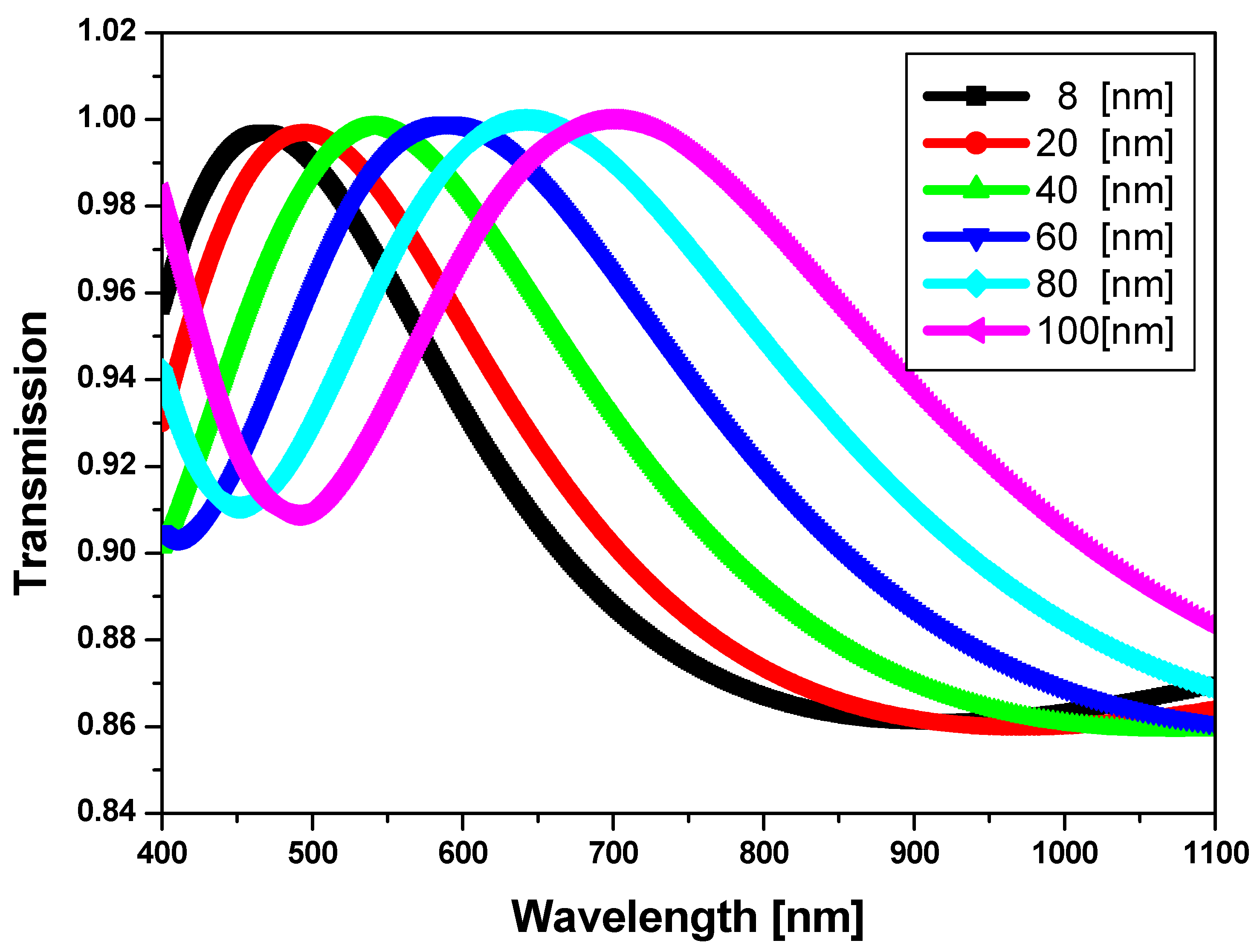
3.1. ARC
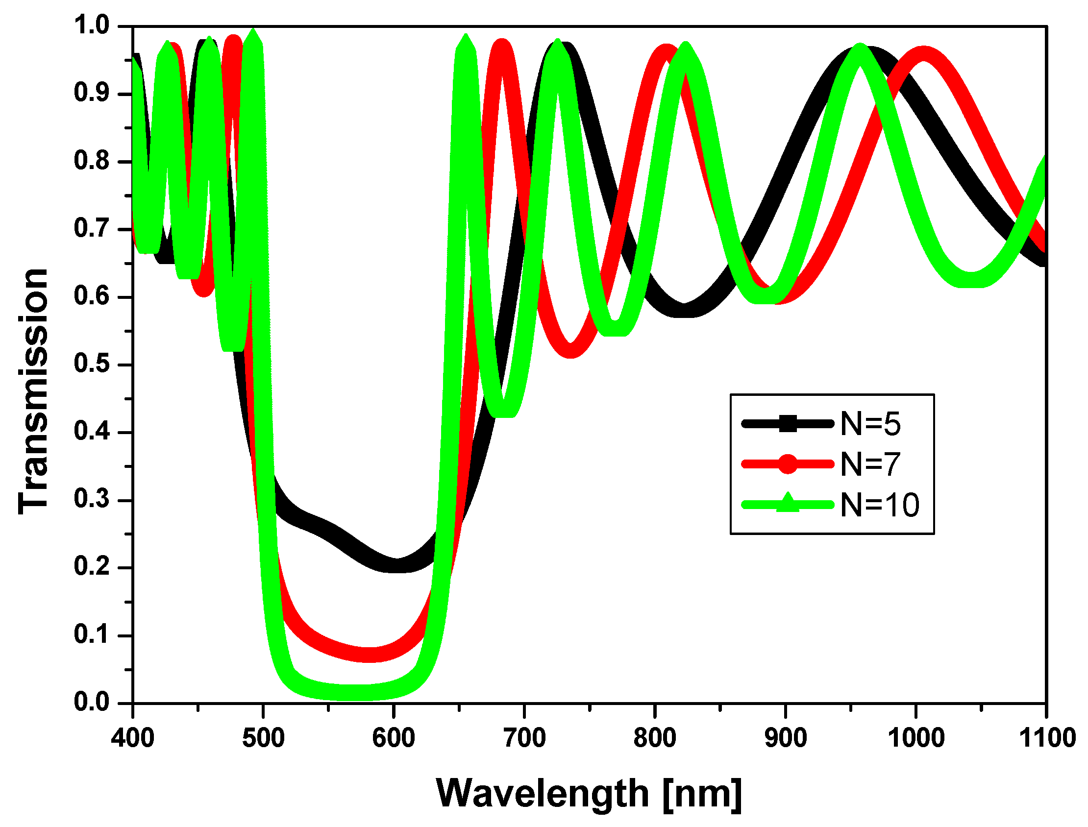
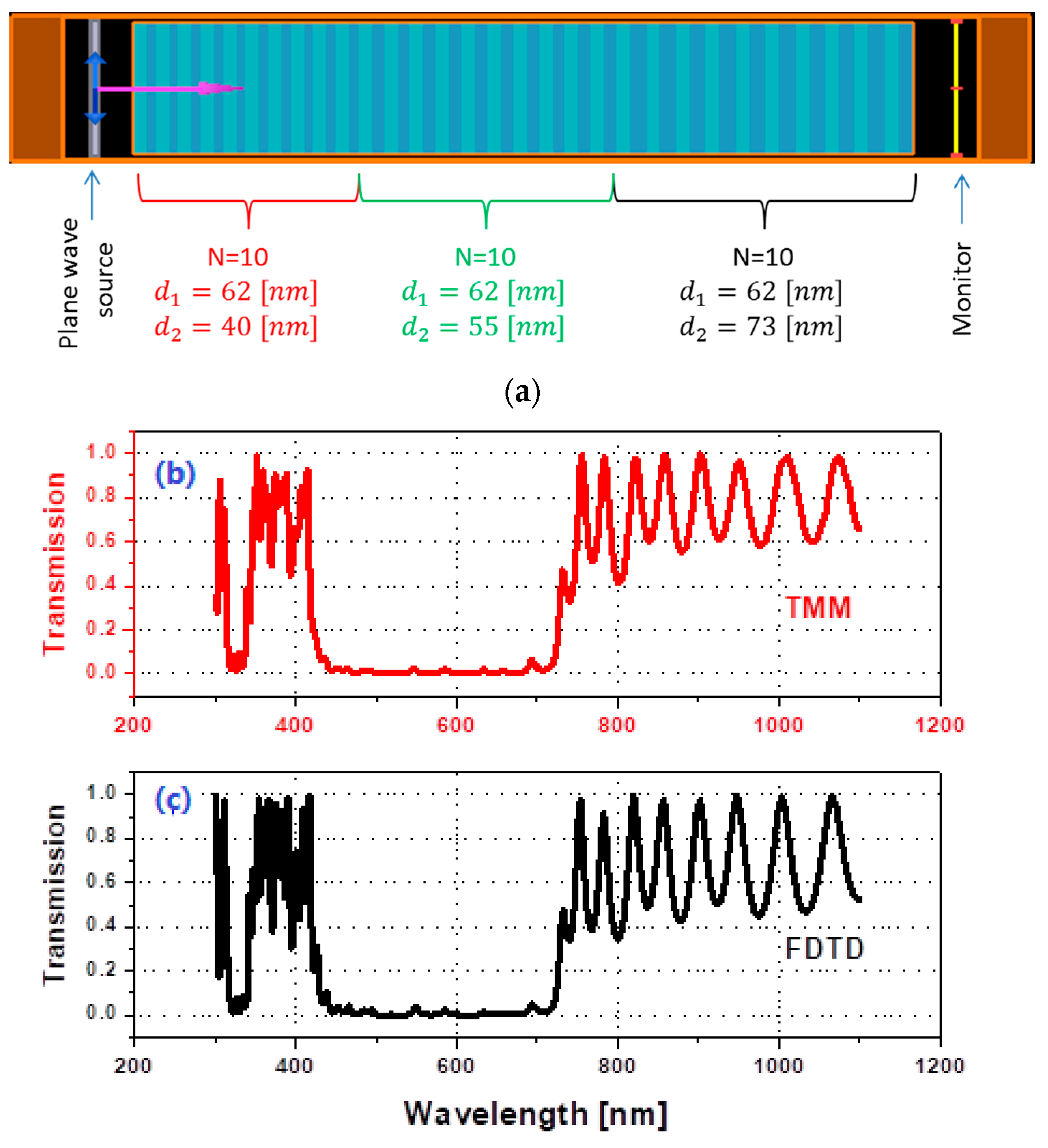
3.2. IRL
4. Conclusions
Author Contributions
Funding
Data Availability Statement
Conflicts of Interest
References
- Sai, H.; Matsui, T.; Saito, K.; Kondo, M.; Yoshida, I. Photocurrent enhancement in thin film silicon solar cells by combination of anti-reflective sub-wavelength structures and light-trapping textures. Prog. Photovolt. 2015, 23, 1572–1580. [Google Scholar] [CrossRef]
- Guo, K.W. Green nanotechnology of trends in future energy: A review. Int. J. Energy Res. 2012, 36, 1–17. [Google Scholar] [CrossRef]
- Herzinger, C.; Johs, B.; McGahan, W.; Woollam, J.; Paulson, W. Ellipsometric determination of optical constants for silicon and thermally grown silicon dioxide via a multi-sample, multi-wavelength, multi-angle investigation. J. Appl. Phys. 1998, 83, 3323–3336. [Google Scholar] [CrossRef]
- Kuang, P.; Eyderman, S.; Hsieh, M.L.; Post, A.; John, S.; Lin, S.Y. Achieving an accurate surface profile of a photonic crystal for near-unity solar absorption in a super thin film architecture. Acs Nano 2016, 10, 6116–6124. [Google Scholar] [CrossRef]
- Lin, Y.Y.; Xu, Z.; Yu, D.L.; Lu, L.F.; Yin, M.; Tavakoli, M.M.; Chen, X.Y.; Hao, Y.Y.; Fan, Z.Y.; Cui, Y.X.; et al. Dual-layer nanostructured flexible thin-film amorphous silicon solar cells with enhanced light harvesting and photoelectric conversion efficiency. ACS Appl. Mater. Interfaces 2016, 8, 10929–10936. [Google Scholar] [CrossRef] [PubMed]
- Kuang, P.; Deinega, A.; Hsieh, M.-L.; John, S.; Lin, S.-Y. Light trapping and near-unity solar absorption in a three-dimensional photonic-crystal. Opt. Lett. 2013, 38, 4200. [Google Scholar] [CrossRef] [Green Version]
- Aly, A.H.; Sayed, H. Computer simulation and modeling of solar energy based on photonic band gap materials. Opt. Appl. (OA) 2018, 48, 117–126. [Google Scholar]
- Sprafke, A.N.; Wehrspohn, R.B. Light Trapping Concepts for Photon Management in Solar Cells. Green 2012, 2, 177–187. [Google Scholar] [CrossRef]
- Green, M. Third Generation Photovoltaics Advanced Solar Energy Conversion; Springer: Berlin/Heidelberg, Germany, 2003. [Google Scholar]
- Li, T. Enhancement of light absorption in thin film silicon solar cells with light traping. Chin. J. Lumin. 2016, 37, 816–822. [Google Scholar]
- Rand, B.; Peumans, P.; Forrest, S.R. Long-range absorption enhancement in organic tandem thin-film solar cells containing silver nanoclusters. J. Appl. Phys. 2012, 96, 7519. [Google Scholar] [CrossRef]
- Brendel, R.; Hirsch, M.; Plieninger, R.; Werner, J. Quantum efficiency analysis of thin-layer silicon solar cells with back surface fields and optical confinement. IEEE Trans. Electron Devices 1996, 43, 1104–1113. [Google Scholar] [CrossRef]
- Wehrspohn, R.B.; Upping, J.; Beckers, T.; Carius, R. 3D Photonic Crystals for Photon Management in Solar Cells; SPIE: Bellingham, WA, USA, 2011. [Google Scholar]
- Yamamoto, K.; Yoshimi, M.; Tawada, Y.; Fukuda, S.; Sawada, T.; Meguro, T.; Takata, H.; Suezaki, T.; Koi, Y.; Hayashi, K.; et al. Large area thin film Si module. Sol. Energy Mater. Solar Cells 2002, 74, 449–455. [Google Scholar] [CrossRef]
- Narasimhan, V.K.; Cui, Y. Nanostructures for photon management in solar cells. Nanophotonics 2013, 2, 87–210. [Google Scholar] [CrossRef]
- Aly, A.H.; Sayed, H. Enhancement of the solar cell based on nanophotonic crystals. J. Nanophotonics 2017, 11, 046020. [Google Scholar] [CrossRef]
- Aly, A.H.; Sayed, H. Photonic band gap materials and monolayer Solar cell. Surf. Rev. Lett. 2018, 25, 1850103. [Google Scholar] [CrossRef]
- Foster, S.; John, S. Light-trapping design for thin-film silicon-perovskite tandem solar cells. J. Appl. Phys. 2016, 120, 103103. [Google Scholar] [CrossRef] [Green Version]
- Yablonovitch, E. Inhibited Spontaneous Emission in Solid-State Physics and Electronics. Phys. Rev. Lett. 1987, 58, 2059–2062. [Google Scholar] [CrossRef] [Green Version]
- Chutinan, A.; Kherani, N.P.; Zukotynski, S. High-efficiency photonic crystal solar cell architecture. Opt. Express 2009, 17, 8871–8878. [Google Scholar] [CrossRef] [PubMed]
- Liu, W.; Ma, H.; Walsh, A. Advance in photonic crystal solar cells. Renew. Sustain. Energy Rev. 2019, 116, 109436. [Google Scholar] [CrossRef]
- Aly, A.H.; Hsu, H.T.; Yang, T.J.; Wu, C.J.; Hwangbo, C.K. Extraordinary optical properties of a superconducting periodic multilayer near zero permittivity operation range. J. Appl. Phys. 2009, 105, 083917-6. [Google Scholar] [CrossRef] [Green Version]
- Aly, A.H.; Elsayed, H.A.; Hamdy, H.S. The optical transmission characteristics in metallic photonic crystals. Mater. Chem. Phys. 2010, 124, 856–860. [Google Scholar] [CrossRef]
- Trabelsi, Y.; Belhadj, W.; Ali, B.; Aly, A.H. Theoretical Study of Tunable Optical Resonators in Periodic and Quasiperiodic One-Dimensional Photonic Structures Incorporating a Nematic Liquid Crystal. Photonics 2021, 8, 150. [Google Scholar] [CrossRef]
- A Ameen, A.; A Elsayed, H.; Alamri, S.; Matar, Z.; Al-Dossari, M.; Aly, A.H. Towards Promising Platform by Using Annular Photonic Crystals to Simulate and Design Useful Mask. Photonics 2021, 8, 349. [Google Scholar] [CrossRef]
- Green, M.A. Silicon solar cells: Evolution, high-efficiency design and efficiency enhancements. Semicond. Sci. Technol. 1993, 8, 1–12. [Google Scholar] [CrossRef]
- Chattopadhyay, S.; Huang, Y.; Jen, Y.; Ganguly, A.; Chen, K.-H.; Chen, L. Anti-reflecting and photonic nanostructures. Mater. Sci. Eng. R: Rep. 2010, 69, 1–35. [Google Scholar] [CrossRef]
- Rajteri, M.; Rastello, M.; Monticone, E. Antireflection coatings for superconducting photodetectors. Nucl. Instruments Methods Phys. Res. Sect. A: Accel. Spectrometers, Detect. Assoc. Equip. 2000, 444, 461–464. [Google Scholar] [CrossRef]
- Zhao, J.; Green, M. Optimized antireflection coatings for high-efficiency silicon solar cells. IEEE Trans. Electron Devices 1991, 38, 1925–1934. [Google Scholar] [CrossRef]
- Anderson, M.J.; Whitcomb, P.J. Design of Experiments. In Encyclopedia of Chemical Technology; Kirk, R.E., Othmer, D.F., Eds.; John Wiley & Sons, Inc.: Hoboken, NJ, USA, 2000. [Google Scholar]
- Yang, L.; Liu, Y.; Wang, Y.; Chen, W.; Chen, Q.; Wu, J.; Kuznetsov, A.; Du, X. 18.87%-efficient inverted pyramid structured silicon solar cell by one-step Cu-assisted texturization technique. Sol. Energy Mater. Sol. Cells 2017, 166, 121–126. [Google Scholar] [CrossRef] [Green Version]
- Domínguez, S.; García, O.; Ezquer, M.; Rodríguez, M.J.; Lagunas, A.R.; Pérez-Conde, J.; Bravo, J. Optimization of 1D photonic crystals to minimize the reflectance of silicon solar cells. Photonics Nanostructures Fundam. Appl. 2012, 10, 46–53. [Google Scholar] [CrossRef]
- Bermel, P.; Luo, C.; Zeng, L.; Kimerling, L.C.; Joannopoulos, J.D. Improving thin-film crystalline silicon solar cell efficiencies with photonic crystals. Opt. Express 2007, 15, 16986–17000. [Google Scholar] [CrossRef]
- Zhang, S.; Zhao, H.; Li, X.; Li, Y.; Jin, Y.; Liu, X.; Shi, G.; Wong, P.K. A hierarchical SiPN/CN/MoSx photocathode with low internal resistance and strong light-absorption for solar hydrogen production. Appl. Catal. B Environ. 2021, 300, 120758. [Google Scholar] [CrossRef]
- Jin, X.; Zhu, Q.; Feng, L.; Li, X.; Zhu, H.; Miao, H.; Zeng, Z.; Wang, Y.; Li, Y.; Wang, L.; et al. Light-Trapping SERS Substrate with Regular Bioinspired Arrays for Detecting Trace Dyes. ACS Appl. Mater. Interfaces 2021, 13, 11535–11542. [Google Scholar] [CrossRef]
- Li, X.; Li, Y.; Wang, H.; Miao, H.; Zhu, H.; Liu, X.; Lin, H.; Shi, G. Fabrication of a Three-Dimensional Bionic Si/TiO2/MoS2 Photoelectrode for Efficient Solar Water Splitting. ACS Appl. Energy Mater. 2021, 4, 730–736. [Google Scholar] [CrossRef]
- Zhou, S.; Wang, S.; Zhou, S.; Xu, H.; Zhao, J.; Wang, J.; Li, Y. An electrochromic supercapacitor based on an MOF derived hierarchical-porous NiO film. Nanoscale 2020, 12, 8934–8941. [Google Scholar] [CrossRef] [PubMed]
- Xu, H.; Liu, L.; Teng, F.; Lu, N. Emission Enhancement of Fluorescent Molecules by Antireflective Arrays. Research 2019, 2019, 1–8. [Google Scholar] [CrossRef] [Green Version]
- Xu, H.; Lu, N.; Qi, D.; Hao, J.; Gao, L.; Zhang, B.; Chi, L. Biomimetic Antireflective Si Nanopillar Arrays. Small 2008, 4, 1972–1975. [Google Scholar] [CrossRef] [PubMed]
- Sai, H.; Fujii, H.; Arafune, K.; Ohshita, Y.; Yamaguchi, M.; Kanamori, Y.; Yugami, H. Antireflective subwavelength structures on crystalline Si fabricated using directly formed anodic porous alumina masks. Appl. Phys. Lett. 2006, 88, 201116. [Google Scholar] [CrossRef]
- Sun, C.H.; Min, W.L.; Linn, N.C.; Jiang, P.; Jiang, B. Templated fabrication of large area subwavelength antireflection gratings on silicon. Appl. Phys. Lett. 2007, 91, 231105. [Google Scholar] [CrossRef]
- Sun, C.H.; Gonzalez, A.; Linn, N.C.; Jiang, P.; Jiang, B. Broadband moth-eye antireflection coatings on silicon. Appl. Phys. Lett. 2008, 92, 061112. [Google Scholar] [CrossRef] [Green Version]
- Chang, Y.-J.; Chen, Y.-T. Broadband omnidirectional antireflection coatings for metal-backed solar cells optimized using simulated annealing algorithm incorporated with solar spectrum. Opt. Express 2011, 19, A875–A887. [Google Scholar] [CrossRef]
- Mackay, T.G.; Lakhtakia, A. The Transfer-Matrix Method in Electromagnetics and Optics. Morgan Claypool 2020, 1, 1–26. [Google Scholar] [CrossRef]
- Chern, G.W.; Wang, L.A. Transfer-matrix method based on perturbation expansion for periodic and quasi-periodic binary long-period gratings. J. Opt. Soc. Am. A 1999, 16, 2675–2689. [Google Scholar] [CrossRef]
- Archambeault, B.; Ramahi, O.M.; Brench, C. The Finite-Difference Time-Domain Method. In EMI/EMC Computational Modeling Handbook; Springer: Boston, MA, USA, 1998. [Google Scholar]
- Sheng, X.-Q.; Song, W. Finite-Difference Time-Domain Method. In Essentials of Computational Electromagnetics; IEEE: Piscataway, NJ, USA, 2012; pp. 207–241. [Google Scholar]
- Yeng, Y.X.; Chou, J.B.; Rinnerbauer, V.; Shen, Y.; Kim, S.G.; Joannopoulos, J.D.; Soljacic, M.; Celanovi, I. Global optimization of omnidirectional wavelength selective emitters/absorbers based on dielectric-filled anti-reflection coated two-dimensional metallic photonic crystals. Opt. Express 2014, 22, 21711–21718. [Google Scholar] [CrossRef] [PubMed]
- Mutitu, J.G.; Shi, S.; Chen, C.; Creazzo, T.; Barnett, A.; Honsberg, C.; Prather, W. Thin film silicon solar cell design based on photonic crystal and diffractive grating structures. Opt. Soc. Am. 2008, 16, 15238–15248. [Google Scholar]
- Deinega, A.; John, S. Effective optical response of silicon to sunlight in the finite-difference time-domain method. Opt. Lett. 2011, 37, 112–114. [Google Scholar] [CrossRef] [PubMed] [Green Version]
- Rajib, M.R.H.; Rana, S.M.; Hasan, M.R.; Amin, R.; Iqbal, M.S.; Anik, M.R.K.; Mia, M.N.H.; Hoq, M.; Hasan, M. Simulation of Mono Layer Solar Cell Using COMSOL and Fabrication in Particle Controlled BAEC Clean Room. Int. J. Eng. Res. Technol. (IJERT) 1973, 3, 295–300. [Google Scholar]
- Banerjee, A. Enhanced Temperature Sensing by Using One-Dimensional Ternary Photonic Band Gap Structures. Prog. Electromagn. Res. Lett. 2009, 11, 129–137. [Google Scholar] [CrossRef] [Green Version]
- Hoffmann, A.; Paetzold, U.W.; Zhang1, C.; Merdzhanova, T.; Lambertz, A.; Ulbrich, C.; Bittkau, K.; Rau, U. Advancing tandem solar cells by spectrally selective multilayer intermediate reflectors. Opt. Express 2014, 22, A1270–A1277. [Google Scholar] [CrossRef]
- Philip, H.R. Optical properties of silicon nitride. J. Electrochim. Soc. 1973, 120, 295–300. [Google Scholar] [CrossRef]
- Podlucký, L.; Vincze, A.; Kováčová, S.; Chlpík, J.; Kováč, J.; Uherek, F. Optimization of Fabrication Process for SiON/SiOx Films Applicable as Optical Waveguides. Coatings 2021, 11, 574.010D. [Google Scholar] [CrossRef]
- Tu, Y.-C.; Wang, S.-J.; Wu, C.-H.; Chang, K.-M.; Lin, T.-H.; Hung, C.-H.; Wu, J.-S. Improving Crystalline Silicon Solar Cell Efficiency Using Graded-Refractive-Index SiON/ZnO Nanostructures. Int. J. Photoenergy 2015, 2015, 1–6. [Google Scholar] [CrossRef] [Green Version]
- Defranoux, C.; Piel, J.; Stehle, J. Deep ultra-violet measurements of SiON antireflective Coatings by spectroscopic ellipsometry. Thin Solid Films 1998, 313–314, 742–744. [Google Scholar] [CrossRef]
- Park, S.; Park, H.; Kim, D.; Nam, J.; Yang, J.; Lee, D.; Min, B.K.; Kim, K.N.; Park, S.J.; Kim, S.; et al. Continuously deposited anti-reflection double layer of silicon nitride and silicon oxynitride for selective emitter solar cells by PECVD. Curr. Appl. Phys. 2017, 17, 517–521. [Google Scholar] [CrossRef]
- Wörhoff, K.; Driessen, A.; Lambeck, P.; Hilderink, L.; Linders, P.; Popma, T. Plasma enhanced chemical vapor deposition silicon oxynitride optimized for application in integrated optics. Sensors Actuators A Phys. 1999, 74, 9–12. [Google Scholar] [CrossRef]
- Huang, C.S.; Huang, C.; Chen, C.T.; Lin, S.C.; Kuo, L. SiON AR layer application for silicon solar cells. In Proceedings of the Conference Record of the Twenty-Ninth IEEE Photovoltaic Specialists Conference, New Orleans, LA, USA, 19–24 May 2002. [Google Scholar]
- Sun, X.; Chen, X.; Zhang, Z.; Sun, Z. Plasmon based antireflection coatings containing nanostructured Ag and silica medium. Appl. Surf. Sci. 2012, 258, 3785–3788. [Google Scholar] [CrossRef]
- Nguyen, H.T.T.; Balaji, N.; Park, C.; Triet, N.M.; Le, A.H.T.; Lee, S.; Jeon, M.; Oh, D.; Dao, V.A.; Yi, J. Al2O3/SiON stack layers for effective surface passivation and anti-reflection of high efficiency n-type c-Si solar cells. Semicond. Sci. Technol. 2017, 32, 025005. [Google Scholar] [CrossRef]
- Domínguez, S.; Cornago, I.; García, O.; Ezquer, M.; Rodríguez, M.J.; Lagunas, A.R.; Pérez-Conde, J.; Bravo, J. Design, optimization and fabrication of 2D photonic crystals for solar cells. Photonics Nanostructures Fundam. Appl. 2013, 11, 29–36. [Google Scholar] [CrossRef]
- Aly, A.H.; Sayed, H.; Elsayed, H.A. Development of the Monolayer Silicon Solar Cell Based on Photonic Crystals. Silicon 2018, 11, 1377–1382. [Google Scholar] [CrossRef]
- Elsayed, H.A.; Sayed, H.; Taha, T.; Alharbi, A.G.; Alenad, A.M.; Alshammari, B.A.; Ahmed, A.M.; Mehaney, A.; Aly, A.H. Simple and efficient design towards a significant improvement of the optical absorption of amorphous silicon solar cell. J. Quant. Spectrosc. Radiat. Transf. 2021, 275, 107890. [Google Scholar] [CrossRef]
- Zhu, J.; Yu, Z.; Fan, S.; Cui, Y. Nanostructured photon management for high performance solar cells. Mater. Sci. Eng. R: Rep. 2010, 70, 330–340. [Google Scholar] [CrossRef]
- Zaidi, S.H.; Gee, J.M.; Ruby, D.S. Diffraction grating structures in solar cells. In Proceedings of the Photovoltaic Specialists Conference, Anchorage, AK, USA, 15–22 September 2000; pp. 395–398. [Google Scholar]


| Anti-Reflection Coating Design | Average Reflectance (%) [400–1000 nm] | Average Reflectance (%) [500–700 nm] | Reference |
|---|---|---|---|
| Polished silicon | 33.4 | 35.88 | [7,8] |
| Standard Silicon solar cell | 16.75 | 16.23 | [31] |
| Rectangular PC profile | 15.04 | 15.9 | [32] |
| Triangular PC profile | 10.68 | 10.6 | [32,66] |
| Circular PC profile | 16.99 | 17.13 | [32] |
| 1D rectangular PC | 23.25/15.26 | 26/14.08 | [66] |
| 1D triangular PC | 6.93/19.95 | 7.01/16.62 | [67] |
| 1D planner PCs | 8 | 6 | Our work |
Publisher’s Note: MDPI stays neutral with regard to jurisdictional claims in published maps and institutional affiliations. |
© 2021 by the authors. Licensee MDPI, Basel, Switzerland. This article is an open access article distributed under the terms and conditions of the Creative Commons Attribution (CC BY) license (https://creativecommons.org/licenses/by/4.0/).
Share and Cite
Sayed, H.; Matar, Z.S.; Al-Dossari, M.; Amin, A.F.; El-Gawaad, N.S.A.; Aly, A.H. The Design and Optimization of an Anti-Reflection Coating and an Intermediate Reflective Layer to Enhance Tandem Solar Cell Photons Capture. Crystals 2022, 12, 57. https://doi.org/10.3390/cryst12010057
Sayed H, Matar ZS, Al-Dossari M, Amin AF, El-Gawaad NSA, Aly AH. The Design and Optimization of an Anti-Reflection Coating and an Intermediate Reflective Layer to Enhance Tandem Solar Cell Photons Capture. Crystals. 2022; 12(1):57. https://doi.org/10.3390/cryst12010057
Chicago/Turabian StyleSayed, Hassan, Z. S. Matar, M. Al-Dossari, A. F. Amin, N. S. Abd El-Gawaad, and Arafa H. Aly. 2022. "The Design and Optimization of an Anti-Reflection Coating and an Intermediate Reflective Layer to Enhance Tandem Solar Cell Photons Capture" Crystals 12, no. 1: 57. https://doi.org/10.3390/cryst12010057
APA StyleSayed, H., Matar, Z. S., Al-Dossari, M., Amin, A. F., El-Gawaad, N. S. A., & Aly, A. H. (2022). The Design and Optimization of an Anti-Reflection Coating and an Intermediate Reflective Layer to Enhance Tandem Solar Cell Photons Capture. Crystals, 12(1), 57. https://doi.org/10.3390/cryst12010057