Article

Photo-Excited Switchable Terahertz Metamaterial Polarization Converter/Absorber

1
Industries Training Centre, Shenzhen Polytechnic (SZPT), Shenzhen 518055, China
2
College of Electrical and Information Engineering, Hunan University, Changsha 410082, China
*
Author to whom correspondence should be addressed.
Crystals 2021, 11(9), 1116; https://doi.org/10.3390/cryst11091116
Submission received: 9 August 2021 / Revised: 9 September 2021 / Accepted: 10 September 2021 / Published: 14 September 2021
(This article belongs to the Special Issue Robust Microelectronic Devices)

Abstract

:
In this paper, a photo-excited switchable terahertz metamaterial (MM) polarization converter/absorber has been presented. The switchable structure comprises an orthogonal double split-ring resonator (ODSRR) and a metallic ground, separated by a dielectric spacer. The gaps of ODSRR are filled with semiconductor photoconductive silicon (Si), whose conductivity can be dynamically tuned by the incident pump beam with different power. From the simulated results, it can be observed that the proposed structure implements a wide polarization-conversion band in 2.01–2.56 THz with the conversion ratio of more than 90% and no pump beam power incident illuminating the structure, whereas two absorption peaks operate at 1.98 THz and 3.24 THz with the absorption rates of 70.5% and 94.2%, respectively, in the case of the maximum pump power. Equivalent circuit models are constructed for absorption states to provide physical insight into their operation. Meanwhile, the surface current distributions are also illustrated to explain the working principle. The simulated results show that this design has the advantage of the switchable performance afforded by semiconductor photoconductive Si, creating a path towards THz imaging, active switcher, etc.

1. Introduction

Metamaterials (MMs), a class of artificial materials comprised of sub-wavelength periodic or non-periodic structures, have received more and more interest in the past few decades [1] due to their extraordinary characteristics in manipulating electromagnetic (EM) waves unavailable in nature [2]. MMs have been widely used in a variety of functional devices so far, such as absorber [3,4,5,6,7,8], cloak [9,10,11,12], sensor [13,14,15], polarizer [16,17,18,19] and so on.
With the development of terahertz (THz) techniques and materials, various MM-based THz devices have been deployed and designed to manipulate THz waves over the past few decades [20,21,22,23,24]. Among these architectures, in general, the MM structures can be divided into two types: reflection [21,22] and transmission [23,24]. However, most THz devices usually can only work in static (reflection/transmission state), and thus have a single function making them difficult to change once fabricated, which severely hamper their practical applications.
To solve this challenge, MM structures integrated with active media (i.e., active THz devices), such as MEMS [25,26], graphene [27,28,29], vanadium dioxide (VO2) [30,31], indium antimonide (InSb) [32,33] and semiconductors silicon (Si) [34,35], etc., have been presented and designed to realize the dynamic and active manipulation of THz wave under the control of external stimuli, such as electrical biasing, optical illumination and thermal excitation. Among these tunable materials, the photoconductive semiconductors (Si) [36,37] can provide a viable pathway to realize a fast change of the reflection/transmission responses for the incident waves under the excitation of light pulse with its exceptional optical-electrical characteristics, including ultrafast response, low cost and high quantum efficiency.
Recently, several active MM-based THz structures based on photoconductive silicon have been investigated in-depth with a lot of effort [38,39,40,41]. These designs can demonstrate unique advantages, including the operational state, the working frequency and intensity modulation to ensure a fair comparison with existing devices at hand, but these architectures are incapable of realizing the switchable performance between absorption [42,43] and polarization conversion [44,45,46], and it only can work for a single function.
In this paper, a photo-excited switchable MM polarization converter/absorber is proposed with photoconductive silicon (Si), which can be freely and continuously switched from a broadband polarization converter to a dual-band absorber in two different pump beam power. Due to the conductivity of photoconductive Si ( σ S i ) being proportional to the pump power of the incident optical beam, the switchable capability of this structure can be achieved by dynamically adjusting the working state of photoconductive Si. This structure can cover a 24.1% fractional bandwidth of polarization conversion with the polarization-conversion ratio (PCR) >90% as σ S i = 1 S/m, while σ S i is equal to 1 × 10⁵ S/m, where it can behave as a dual-band absorber. The surface current distributions of this design on both top and bottom layers are provided to investigate the switchable operating mechanism for different Si conductivity states. This structure would be poised to act as a suitable alternative to THz sensing, communication and detection, etc., for its excellent characteristics.

2. Metamaterials and Methods

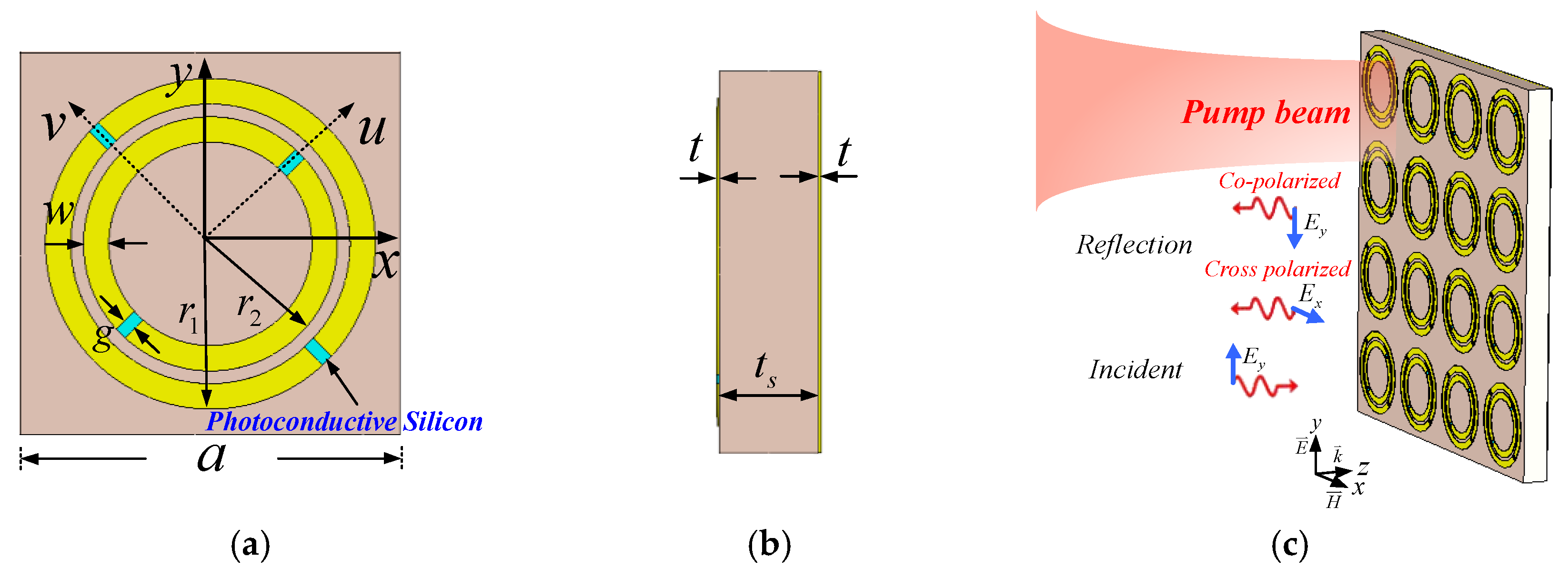
2.1. Metamaterials Model

The unit cell geometry of the proposed structure is shown in Figure 1. From the figure, the structure consists of a top metallic orthogonal double split-ring resonator (ODSRR) and a dielectric substrate with a bottom ground plane. The gold is selected as a metallic model for this structure with a thickness ( t ) of 0.4 μm, and conductivity ( σ ) of 4.561 × 10⁷ S/m. The dielectric layer is polyimide material ( ε r = 3.5 , tan δ = 0.02 ) with a thickness ( t s ) of 6.5 μm. The semiconductor photoconductive Si (blue part) is integrated into the split gaps of ODSRR, which can be modeled as a dielectric material ( ε Si = 11.7 ) with a thickness ( t ) of 0.4 μm, whose conductivity ( σ S i ) changes with variation of the incident pump beam power. Then other geometric parameters of the proposed structure (μm) are a = 30, r 1 = 13.5, r 2 = 10.5, w = 2, g = 0.5.

2.2. Mathematical Method

To better explain the switchable property of the proposed structure, the uv coordinate system is introduced to mark the anisotropic axes, and both u and v axes exhibit 45° phase shifts as compared to the x and y axes, respectively, as shown in Figure 1a. To effectively analyze the polarization characteristic of the polarization converter, the co-polarization and cross-polarized reflections can be defined as r y y = | E r y / E i y | and r x y = | E r x / E i y | for the y-polarized incident wave [47], where the subscripts of i and r represent the incident and reflected wave modes, respectively, and then the subscripts of x and y indicate the electric field directions. The phase difference between the y and x components of the reflected THz wave is also written as Δ ϕ = ϕ x y ϕ y y . To estimate the polarization conversion performance, the polarization rotation azimuth angle φ and the polarization-conversion ratio (PCR) can be extracted from the refection coefficients [48] to be targeted as goal metrics during design. Therefore, φ can be calculated as:
φ = 1 2 acr tan [ 2 R cos ( Δ ϕ ) 1 R 2 ]
where R = | r x y | / | r y y | and PCR can be obtained in the following manner:
P C R = | r x y | 2 | r x y | 2 + | r y y | 2
As the bottom layer is a metallic plane, the transmission is nearly zero and, thus, the absorptivity of this design can be defined as:
A = 1 R = 1 ( | r x y | 2 + | r y y | 2 )

3. Results and Discussions

To demonstrate the switchable performance of this structure, the numerical model is constructed to simulate with the commercial full-wave solver, software CST Microwave Studio, for two different Si conductivity ( σ S i ) states. In the simulation setting, the periodic boundary conditions (PBC) oriented along the x and y directions is used to model the periodic structure with a normal wave incident upon the unit cell with the E-field vector in the y axis, as described in detail in Figure 1c, behaving as the exciting source.

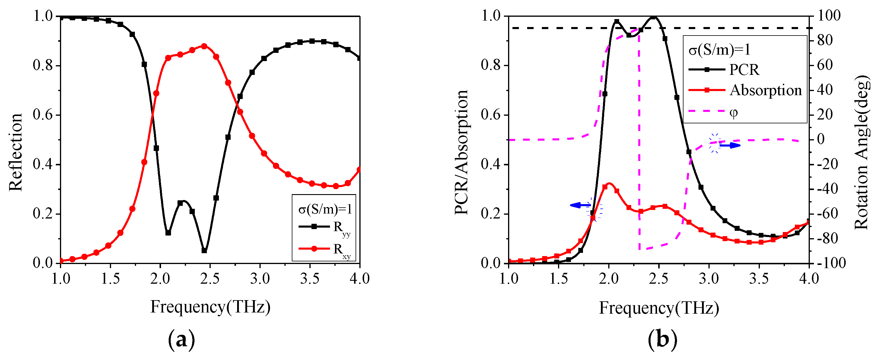
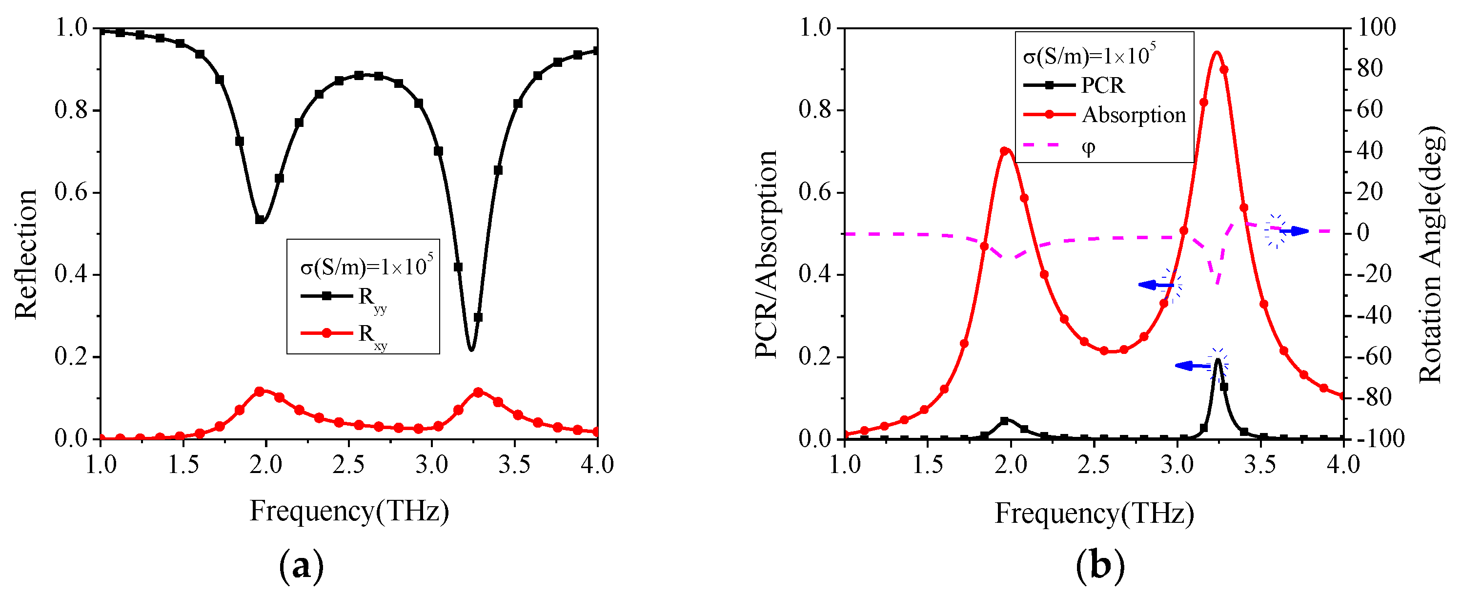
3.1. Reflection Responses

The simulated reflection responses as a function of frequency for two different conductivity states are illustrated in Figure 2 and Figure 3. In the case of σ S i = 1 S/m without pump beam power, the cross-polarization r x y is much greater than the co-polarization r y y across the operating band of 1.8–2.7 THz as plotted in Figure 2a. In Figure 2b, it can be seen that PCR is more than 0.9 in the frequency range of 2.01–2.56 THz with an absorption rate less than 0.3. Meanwhile, the rotation azimuth angle is approximately around ±90° in this band, forming a broad cross-polarization conversion bandwidth. Hence, for this case, the designed structure can be referred to as a broad polarization converter.
With the maximal pump beam power incident on the structure, σ S i can reach up to 1 × 10⁵ S/m, termed mental state, such that the Si-filled gaps would be in short circuit state, then the cross-polarization r x y is less than the co-polarization r y y over the whole frequency band as observed from Figure 3a. From the results in Figure 3b, the PCR is below 0.2 at the two resonant peaks of 1.98 THz and 3.24 THz, respectively, and the corresponding absorption rates are around 70.5% and 94.2%, respectively, with the rotation azimuth angles less than 20° across the whole frequency band. Thereby, the structure could be used as a dual-band absorber. Thus, this proposed hybrid metal-semiconductor ODSRR structure could be switched to a polarization converter or absorber by the semiconductor photoconductive Si which can act as the active THz component with different working states under different external pumps’ beam power.

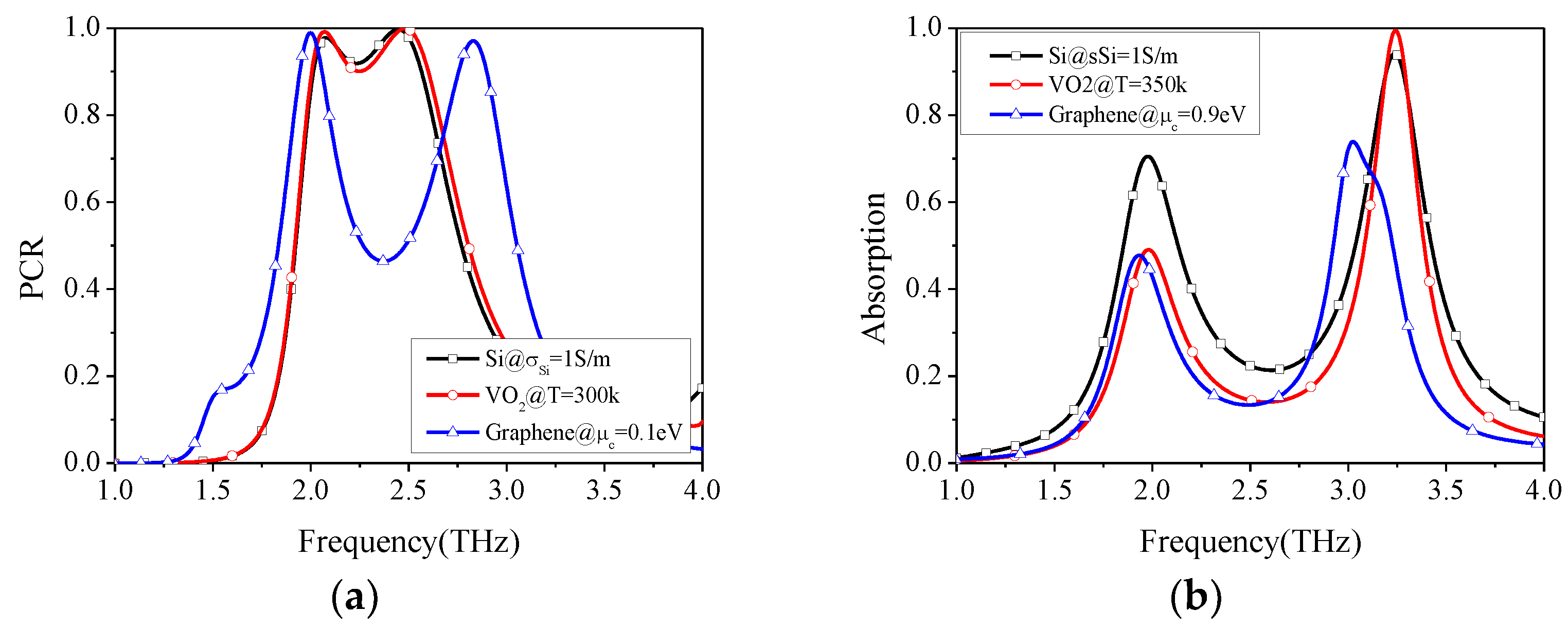
3.2. Validation of the Equivalent Circuit Model

In an attempt to analytically describe the absorption operation, the schematic description of the equivalent circuit model (ECM) for this structure is shown in Figure 4a. The double metallic rings can be represented by distributive elements, whereas the substrate is considered as a transmission line with the length of t s and the wave impedance Z s = Z o / ε r , Z o is the characteristic impedance of the free space. Cm represents the electrical coupling between two double-opening coupling rings [49]. The values of the reactive elements can be approximately calculated as [50,51]:
C i , o = ε o ε e f f 2 a π ln ( csc ( a r 1 , 2 ) π 2 a )
L i , o = μ o μ e f f a 2 π ln ( csc w π 2 a )
where ε o and μ o are the permittivity and permeability of free space, respectively. ε e f f and μ e f f denote the effective permittivity and permeability of the supporting substrate, respectively. The series circuits RLC provide the two absorption responses at 1.98 and 3.24 THz, respectively.
Then, the impedance of the top ODSRR surface can be indicated by Z F , which is in parallel with Z s . Therefore, the input impedance and reflection coefficient from this designed absorber can be respectively calculated as:
Z i n = Z F | | j Z s tan ( β t s )
S 11 = 20 log ( Z i n Z o Z i n + Z o )
To better validate the availability of ECM, the reflection characteristics calculated from the full-wave simulation in CST and the circuit model have been achieved for comparison below in Figure 4b, where good agreement can be seen between the two methods, sufficient to indicate the fact that the ECM used for the modeling method is valid and that results from the mathematical simulations constitute good predictions.

3.3. The Intrinsic Operation Mechanism

Meanwhile, to gain some insight on the working principle of switchable operation of this architecture, the surface current distributions on both top and bottom layers as σ S i = 1 S/m and σ S i = 1 × 10⁵ S/m under normal incidence are plotted in Figure 5 and Figure 6, respectively, at four different frequencies, in which the arrows represent the direction of current flow and the color corresponds with the intensity.
As σ S i = 1 S/m, the surface current distributions at the frequencies of 2.08 and 2.45 THz are described in Figure 5. For y-polarized incident EM wave, the induced surface currents at the top and bottom layers are in the anti-parallel direction, thus forming a circulating loop and exciting a magnetic resonance along the u-direction at 2.08 THz, which can generate the in-phase reflection E i v , but instead E i u is an out-of-phase reflection due to no v-direction magnetic resonance occurring. Hence, the −90° polarization rotation will be implemented, and then the polarization direction of reflection response is converted from y to x-axis at the resonant frequency. Similarly, the magnetic resonance operates at 2.45 THz with the E-field oriented along the v direction, providing the out-of-phase and in-phase reflections for E i v and E i u , respectively. Therefore, the y-to-x polarized reflection will be realized with 90° rotation.
As σ S i = 1 × 10⁵ S/m for the maximal pump beam power case, the Si-filled gaps of the ODSRR structure are short-circuited since the semiconductor Si is in the conducting state. Thus, the ODSRR is treated as a double-ring resonator to lead to the high absorption performance. As observed from Figure 6, for the y-polarized incident wave, the surface currents mainly focus on the left and right sides of the outer ring at 1.98 THz, and at the frequency of 3.24 THz, the surface currents are also mainly distributed at the left and right arms of the inner ring. All these two absorption responses have a similar current distribution with that of the conventional ring-shaped MA, so it is worth noting that the absorption responses are originated from the two arranged dipoles. Therefore, the proposed structure possesses the ability to conduct the switching state between the broadband polarization converter and dual-band absorber for two different states.

3.4. Oblique Incidence Characteristics

Figure 7 shows the oblique incidence characteristics for different Si conductivity (i.e., σ S i = 1 S/m and σ S i = 1 × 10⁵ S/m). From the results, it can be seen that the switchable structure maintains a wide operating bandwidth over the angle range from 0° to 45° with good PCRs of over 75% for both TE and TM waves in Figure 7a,b with σ S i = 1 S/m. Figure 7c,d describe the absorption responses against incident angle ( θ , the angle between the incident wave vector k and the z-axis) varying from 0° to 60° as σ S i = 1 × 10⁵ S/m. In TE mode, the lower resonant frequency shifts slightly to the high frequency as θ goes up at 1.98 THz in Figure 7c, with the absorptivity gradually increasing. It can be ascribed to the strong electrical coupling between the outer and inner rings. On the contrary, the absorption performance is gradually deteriorated with θ changing at the upper frequency of 3.24 THz because the parallel H-field component decreases. For TM mode, the structure shows good angular stability when θ reaches up to 45° as detailed in Figure 7d. Though there is a slight frequency discrepancy (0.06 THz and 0.1 THz for TE and TM mode waves, respectively) for the lower absorption frequency, the upper absorption peak has better angular robustness than that of this absorption peak for different incidents’ wave modes.
A comparison with the current three materials, photoconductive Si, VO2 and graphene embedded in structure to exhibit the switchable performance is illustrated in Figure 8. It is clearly apparent that the proposed design has achieved a better stable switching characteristic than the other two. Comparing to the VO2, photoconductive Si can maintain insensitive to the external temperature of the surrounding environment and provides a robust switchable relative to graphene.

4. Conclusions

A photo-excited switchable THz MTM polarization converter/absorber based on the incorporation of photoconductive Si has been designed and demonstrated in this paper. The conductivity of Si is dynamically adjusted by the external incident pump power, applied to provide a means of achieving the polarization modulation for the reflected waves. The novelty of the structure lies in its switchable performance as compared with the previous works. This design has its unique advantage of cross-polarization conversion with a relative bandwidth of 24.1% (PCR >90%) as σ S i = 1 S/m without pump beam and acting as the dual-band absorber under the case of σ S i = 1 × 10⁵ S/m with maximal pump optical illuminating power. The design has opened up a new field towards active switches and polarization manipulation with high performance in the THz regime. Therefore, this photo-excited switchable MTM polarization converter/absorber can be potentially applied to biological imaging, THz scanning, sensors, and so on.

Author Contributions

This study was conducted through the contributions of all authors. Conceptualization, investigation, validation, D.Y. and Y.D.; software, Y.R. and G.L. (Guochao Li); writing—original draft preparation, D.Y. and Y.D.; writing—review and editing, G.L. (Gaosheng Li) and H.M.; visualization, S.D.; supervision, Z.L. All authors have read and agreed to the published version of the manuscript.

Funding

This work was supported by the Young Creative Talents Project of Guangdong Provincial Department of Education under grant number 2020KQNCX203.

Institutional Review Board Statement

Not applicable.

Informed Consent Statement

Not applicable.

Data Availability Statement

Not applicable.

Acknowledgments

This work was supported by the Young Creative Talents Project of Guangdong Provincial Department of Education under Grant No. 2020KQNCX203.

Conflicts of Interest

The authors declare no conflict of interest.

References

  1. Engheta, N. Metamaterials with high degrees of freedom: Space, time, and more. Nanophotonics 2020, 10, 639–642. [Google Scholar] [CrossRef]
  2. Xiao, S.; Wang, T.; Liu, T.; Zhou, C.; Jiang, X.; Zhang, J. Active metamaterials and metadevices: A review. J. Phys. D Appl. Phys. 2020, 53, 503002. [Google Scholar] [CrossRef]
  3. Deng, G.; Lv, K.; Sun, H.; Yang, J.; Yin, Z.; Li, Y.; Chi, B.; Li, X. An ultrathin, triple-band metamaterial absorber with wide-incident-angle stability for conformal applications at X and Ku frequency band. Nanoscale Res. Lett. 2020, 15, 217. [Google Scholar] [CrossRef] [PubMed]
  4. Yang, D.; Yin, Y.; Zhang, Z.; Li, D.; Cao, Y. Wide-angle microwave absorption properties of multilayer metamaterial fabricated by 3D printing. Mater. Lett. 2020, 281, 128571. [Google Scholar] [CrossRef]
  5. Li, H.; Ji, C.; Ren, Y.; Hu, J.; Qin, M.; Wang, L. Investigation of multiband plasmonic metamaterial perfect absorbers based on graphene ribbons by the phase-coupled method. Carbon 2019, 141, 481–487. [Google Scholar] [CrossRef]
  6. Al-Badri, K.S.L. Design of perfect metamaetiral absorber for microwave applications. Wirel. Pers. Commun. 2021, 1–8. [Google Scholar] [CrossRef]
  7. Wang, J.; Ding, X.; Huang, X.; Wu, J.; Li, Y.; Yang, H. Metamaterials absorber for multiple frequency points within 1 GHz. Phys. Scr. 2020, 95, 065505. [Google Scholar] [CrossRef]
  8. Zhou, B.C.; Wang, D.H.; Ma, J.J.; Li, B.Y.; Zhao, Y.J.; Li, K.X. An ultrathin and broadband radar absorber using metamaterials. Waves Random Complex Media 2021, 31, 911–920. [Google Scholar] [CrossRef]
  9. Magisetty, R.; Raj, A.B.; Datar, S.; Shukla, A.; Kandasubramanian, B. Nanocomposite engineered carbon fabric-mat as a passive metamaterial for stealth application. J. Alloys Compd. 2020, 848, 155771. [Google Scholar] [CrossRef]
  10. Li, W.; Zhang, Y.; Wu, T.; Cao, J.; Chen, Z.; Guan, J. Broadband radar cross section reduction by in-plane integration of scattering metasurfaces and magnetic absorbing materials. Results Phys. 2019, 12, 1964–1970. [Google Scholar] [CrossRef]
  11. Salami, P.; Yousefi, L. Wide-band polarisation-independent metasurface-based carpet cloak. IET Microw. Antennas Propag. 2020, 14, 1983–1989. [Google Scholar] [CrossRef]
  12. Yang, J.; Huang, C.; Wu, X.; Sun, B.; Luo, X. Dual-wavelength carpet cloak using ultrathin metasurface. Adv. Opt. Mater. 2018, 6, 1800073. [Google Scholar] [CrossRef]
  13. Lin, M.; Xu, M.; Wan, X.; Liu, H.; Wu, Z.; Liu, J.; Deng, B.; Guan, D.; Zha, S. Single sensor to estimate DOA with programmable metasurface. IEEE Internet Things J. 2021, 8, 10187–10197. [Google Scholar] [CrossRef]
  14. Cai, J.; Zhou, Y.J.; Yang, X.M. A metamaterials-loaded quarter mode SIW microfluidic sensor for microliter liquid characterization. J. Electromagn. Waves Appl. 2019, 33, 261–271. [Google Scholar] [CrossRef]
  15. Ming-zhen, X.; Yang, Z.; Wei-ling, F.; Jin-chun, H. Microfludic refractive index sensor based on terahertz metamaterials. Spectrosc. Spectr. Anal. 2021, 41, 1039–1043. [Google Scholar]
  16. Zhang, Y.; Tian, Y.; Zhang, Y.; Dai, L.; Liu, S.; Zhang, Y.; Zhang, H. Dual-function polarizer based on hybrid metasurfaces of vanadium dioxide and Dirac semimetals. Opt. Commun. 2020, 477, 126348. [Google Scholar] [CrossRef]
  17. da Silva Paiva, J.L.; da Silva, J.P.; Campos, A.L.P.D.S.; de Andrade, H.D. Using metasurface structures as signal polarisers in microstrip antennas. IET Microw. Antennas Propag. 2019, 13, 23–27. [Google Scholar] [CrossRef]
  18. Yao, Z.; Lu, M.; Zhang, C.; Wang, Y. Dynamically tunable and transmissive linear to circular polarizer based on graphene metasurfaces. JOSA B 2019, 36, 3302–3306. [Google Scholar] [CrossRef]
  19. Khan, S.; Eibert, T.F. A dual-band metasheet for asymmetric microwave transmission with polarization conversion. IEEE Access 2019, 7, 98045–98052. [Google Scholar] [CrossRef]
  20. Zhong, R.; Yang, L.; Liang, Z.; Wu, Z.; Wang, Y.; Ma, A.; Fang, Z.; Liu, S. Ultrawideband terahertz absorber with a graphene-loaded dielectric hemi-ellipsoid. Opt. Express 2020, 28, 28773–28781. [Google Scholar] [CrossRef]
  21. Dong, Y.; Yu, D.; Li, G.; Li, G.; Ma, H. Tunable ultrathin ultrabroadband metamaterial absorber with graphene-stack-based structure at lower terahertz frequency. Phys. E Low-Dimens. Syst. Nanostruct. 2021, 128, 114608. [Google Scholar] [CrossRef]
  22. Liu, H.B.; Hu, C.X.; Wang, Z.L.; Zhang, H.F.; Li, H.M. An ultra-wideband terahertz metamaterial absorber based on the fractal structure. Plasmonics 2020, 16, 263–271. [Google Scholar] [CrossRef]
  23. Zhang, J.; Li, Z.; Shao, L.; Zhu, W. Dynamical absorption manipulation in a graphene-based optically transparent and flexible metasurface. Carbon 2021, 176, 374–382. [Google Scholar] [CrossRef]
  24. Chu, H.; Qi, J.; Xiao, S.; Qiu, J. A thin wideband high-spatial-resolution focusing metasurface for near-field passive millimeter-wave imaging. Appl. Phys. Lett. 2018, 112, 174101. [Google Scholar] [CrossRef]
  25. Zhu, W.M.; Cai, H.; Mei, T.; Bourouina, T.; Tao, J.F.; Lo, G.Q.; Kwong, D.L.; Liu, A.Q. A MEMS tunable metamaterial filter. In Proceedings of the 2010 IEEE 23rd International Conference on Micro Electro Mechanical Systems (MEMS), Hong Kong, China, 24–28 January 2010; Volume 33, pp. 196–199. [Google Scholar]
  26. Ma, F.; Lin, Y.S.; Zhang, X.; Lee, C. Tunable multiband terahertz metamaterials using a reconfigurable electric split-ring resonator array. Light Sci. Appl. 2014, 3, e171. [Google Scholar] [CrossRef] [Green Version]
  27. Kliros, G.S.; Venetis, D.E. Design of a tunable dual-band THz absorber based on metamaterial split-ring resonators coupled to grapheme. In Proceedings of the 2016 IEEE International Semiconductor Conference (CAS), Sinaia, Romania, 10–12 October 2016; pp. 41–44. [Google Scholar]
  28. Liu, C.; Bai, Y.; Ma, X. Design of a tunable dual-band terahertz absorber based on graphene metamaterial. Opt. Eng. 2018, 57, 117105. [Google Scholar] [CrossRef]
  29. Ahmadivand, A.; Gerislioglu, B.; Ramezani, Z. Gated graphene island-enabled tunable charge transfer plasmon terahertz metamodulator. Nanoscale 2019, 11, 8091–8095. [Google Scholar] [CrossRef] [PubMed]
  30. Zhao, Y.; Huang, Q.; Cai, H.; Lin, X.; Lu, Y. A broadband and switchable VO2-based perfect absorber at the THz frequency. Opt. Commun. 2018, 426, 443–449. [Google Scholar]
  31. Wang, S.; Cai, C.; You, M.; Liu, F.; Wu, M.; Li, S.; Bao, H.; Kang, L.; Werner, D.H. Vanadium dioxide based broadband THz metamaterial absorbers with high tunability: Simulation study. Opt. Express 2019, 27, 19436–19447. [Google Scholar] [CrossRef]
  32. Zou, H.; Cheng, Y. Design of a six-band terahertz metamaterial absorber for temperature sensing application. Opt. Mater. 2019, 88, 674–679. [Google Scholar] [CrossRef]
  33. Liu, H.; Ren, G.; Gao, Y.; Zhu, B.; Wu, B.; Li, H.; Jian, S. Tunable terahertz plasmonic perfect absorber based on T-shaped InSb array. Plasmonics 2016, 11, 411–417. [Google Scholar] [CrossRef]
  34. Agarwal, P.; Medwal, R.; Kumar, A.; Asada, H.; Fukuma, Y.; Rawat, R.S.; Battiato, M.; Singh, R. Ultrafast photo-thermal switching of terahertz spin currents. Adv. Funct. Mater. 2021, 31, 2010453. [Google Scholar] [CrossRef]
  35. Zhao, J.; Cheng, Y.; Cheng, Z. Design of a photo-excited switchable broadband reflective linear polarization conversion metasurface for terahertz waves. IEEE Photon. J. 2018, 10, 4600210. [Google Scholar] [CrossRef]
  36. Xu, Z.C.; Wu, L.; Zhang, Y.T.; Xu, D.G.; Yao, J.Q. Photoexcited blueshift and redshift switchable metamaterial absorber at terahertz frequencies. Chin. Phys. Lett. 2019, 36, 124202. [Google Scholar] [CrossRef]
  37. Lang, T.; Shen, T.; Wang, G.; Shen, C. Tunable broadband all-silicon terahertz absorber based on a simple metamaterial structure. Appl. Opt. 2020, 59, 6265–6270. [Google Scholar] [CrossRef] [PubMed]
  38. Bing, P.; Guo, X.; Wang, H.; Li, Z.; Yao, J. Characteristic analysis of a photoexcited tunable metamaterial absorber for terahertz waves. J. Opt. 2019, 48, 179–183. [Google Scholar] [CrossRef]
  39. Song, Z.; Wang, Z.; Wei, M. Broadband tunable absorber for terahertz waves based on isotropic silicon metasurfaces. Mater. Lett. 2019, 234, 138–141. [Google Scholar] [CrossRef]
  40. Zhao, X.; Wang, Y.; Schalch, J.; Duan, G.; Cremin, K.; Zhang, J.; Chen, C.; Averitt, R.D.; Zhang, X. Optically modulated ultra-broadband all silicon metamaterial terahertz absorbers. ACS Photon. 2019, 6, 830–837. [Google Scholar] [CrossRef]
  41. You, X.; Upadhyay, A.; Cheng, Y.; Bhaskaran, M.; Sriram, S.; Fumeaux, C.; Withayachumnankul, W. Ultra-wideband far-infrared absorber based on anisotropically etched doped silicon. Opt. Lett. 2020, 45, 1196–1199. [Google Scholar] [CrossRef]
  42. Cheng, Y.; Liu, J.; Chen, F.; Luo, H.; Li, X. Optically switchable broadband metasurface absorber based on square ring shaped photoconductive silicon for terahertz waves. Phys. Lett. A 2021, 402, 127345. [Google Scholar] [CrossRef]
  43. Wu, J. A polarization insensitive dual-band tunable graphene absorber at the THz frequency. Phys. Lett. A 2020, 384, 126890. [Google Scholar] [CrossRef]
  44. Cheng, Z.; Cheng, Y. A multi-functional polarization convertor based on chiral metamaterial for terahertz waves. Opt. Commun. 2019, 435, 178–182. [Google Scholar] [CrossRef]
  45. Wong, H.; Wang, K.X.; Huitema, L.; Crunteanu, A. Active meta polarizer for terahertz frequencies. Sci. Rep. 2020, 10, 15382. [Google Scholar] [CrossRef]
  46. Sasaki, T.; Nishie, Y.; Kambayashi, M.; Sakamoto, M.; Noda, K.; Okamoto, H.; Kawatsuki, N.; Ono, H. Active terahertz polarization converter using a liquid crystal-embedded metal mesh. IEEE Photon. J. 2019, 11, 1–7. [Google Scholar] [CrossRef]
  47. Liu, X.; Liu, H.; Sun, Q.; Huang, N. Metamaterial terahertz switch based on split-ring resonator embedded with photoconductive silicon. Appl. Opt. 2015, 54, 3478–3483. [Google Scholar] [CrossRef]
  48. Ding, J.; Arigong, B.; Ren, H.; Zhou, M.; Shao, J.; Lin, Y.; Zhang, H. Efficient multiband and broadband cross polarization converters based on slotted L-shaped nanoantennas. Opt. Express 2014, 22, 29143–29151. [Google Scholar] [CrossRef] [PubMed]
  49. Tang, S.C.; Yu, C.H.; Chiou, Y.C.; Kuo, J.T. Extraction of electric and magnetic coupling for coupled symmetric microstrip resonator bandpass filter with tunable transmission zero. In Proceedings of the 2009 Asia Pacific Microwave Conference, Singapore, 7–10 December 2009; pp. 2064–2067. [Google Scholar]
  50. Al-Behadili, A.A.; Mocanu, I.A.; Codreanu, N.; Pantazica, M. Modified split ring resonators sensor for accurate complex permittivity measurements of solid dielectrics. Sensors 2020, 20, 6855. [Google Scholar] [CrossRef] [PubMed]
  51. Sheikh, S. Miniaturized-element frequency-selective surfaces based on the transparent element to a specific polarization. IEEE Antennas Wirel. Propag. Lett. 2016, 15, 1661–1664. [Google Scholar] [CrossRef]
Figure 1. Schemes of the proposed switchable MM polarization converter/absorber structure: (a) The front and (b) side views of the unit cell structure; (c) 2-D array.
Crystals 11 01116 g001
Figure 2. Simulated (a) cross- and co-polarization reflection coefficients and (b) PCR, absorption and rotation angle with σ S i = 1 S/m.
Crystals 11 01116 g002
Figure 3. Simulated (a) cross- and co-polarization reflection coefficients and (b) PCR, absorption and rotation angle with σ S i = 1 × 10⁵ S/m.
Crystals 11 01116 g003
Figure 4. (a) Equivalent transmission-line model of the proposed absorber (circuit parameters: Ci = 0.44 fF, Co = 0.12 fF, Cm = 0.26 fF, Li = 4.42 pH, Lo = 3.04 pH, Ri = 4.60 Ω, Ro = 4.78 Ω); (b) Comparison of reflectivity of the proposed structure calculated by the ECM and simulated in the CST software.
Crystals 11 01116 g004
Figure 5. The surface current distributions on the top and bottom layers at (a) 2.08 and (b) 2.45 THz for σ S i = 1 S/m.
Crystals 11 01116 g005
Figure 6. The surface current distributions on the top and bottom layers at (a) 1.98 and (b) 3.24 THz for σ S i = 1 × 10⁵ S/m.
Crystals 11 01116 g006
Figure 7. The PCR and absorption performances under different incident angles under (a,c) TE and (b,d) TM modes for different states.
Crystals 11 01116 g007
Figure 8. The PCR and absorption performances under different materials for (a) polarization converter and (b) absorber states.
Crystals 11 01116 g008
Publisher’s Note: MDPI stays neutral with regard to jurisdictional claims in published maps and institutional affiliations.

