Article

Transport Mechanism of Enhanced Performance in an Amorphous/Monoclinic Mixed-Phase Ga2O3 Solar-Blind Deep Ultraviolet Photodetector

Chongqing Key Laboratory of Photo-Electric Functional Materials, College of Physics and Electronic Engineering, Chongqing Normal University, Chongqing 401331, China
*
Authors to whom correspondence should be addressed.
H. Liu and H. Li contributed equally to this work.
Crystals 2021, 11(9), 1111; https://doi.org/10.3390/cryst11091111
Submission received: 17 August 2021 / Revised: 31 August 2021 / Accepted: 8 September 2021 / Published: 12 September 2021
(This article belongs to the Special Issue Wide Bandgap Semiconductor Materials and Devices)

Abstract

:
Recently, as an emerging material, ultrawide bandgap Ga2O3 has been investigated extensively in solar-blind deep-ultraviolet (DUV) photodetectors (PDs). High sensitivity and signal-to-noise ratio of PDs are essential for the detection of solar-blind DUV signals; however, such factors are often not mutually compatible. In the present study, an amorphous/monoclinic homogeneous mixed-phase structure was demonstrated to be significantly beneficial in enhancing the comprehensive performance of Ga2O3 solar-blind DUV PDs, especially with respect to sensitivity and the signal-to-noise ratio. Further experimental and theoretical findings provide insights on the transport mechanism of enhanced performance in the mixed-phase Ga2O3 solar-blind DUV PD. For effectively separating the photogenerated carriers, a type-II band alignment between amorphous and crystalline Ga2O3 can be exploited. Furthermore, the change of the barrier height of the mixed-phase interface also has a significant impact on the transport properties of the mixed-phase Ga2O3 PD. Additionally, the potential applications of mixed-phase Ga2O3 PD in high-voltage corona discharge were explored, and clear and stable corona discharge signals were obtained. The results of the present study may promote understanding of DUV photoelectronic devices with various mixed-phase Ga2O3 materials and provide an efficient approach for promoting comprehensive performance in future solar-blind detection applications.

1. Introduction

Solar-blind deep-ultraviolet (DUV, 200~280 nm) photodetectors (PDs) with significant thermal stability and reliability have drawn considerable attention owing to the wide potential applications thereof in civil, military, and scientific research, such as high-voltage corona detection, flame detection, ozone holes monitoring, missile guidance, space communication, biochemical detection, and others [1,2,3,4,5,6]. At present, due to the relatively mature silicon technology, DUV detection is mainly dominated by silicon-based photodiodes [3], photomultiplier tubes (PMTs) [7], and charged-coupled devices (CCDs) [1,7]. However, mature silicon technology has several limitations in solar-blind DUV detection, which can be primarily attributed to the significant loss of the solar-blind region caused by the narrow bandgap of 1.13 eV [2]. In recent years, with the development of wide bandgap (WBG) semiconductor materials and devices, solar-blind DUV-PDs based on WBG materials have emerged, such as AlGaN, MgZnO, ZnGaO, AlN, BN, diamond, and gallium oxide (Ga2O3) [4,8,9]. Among said materials, in addition to Ga2O3, other materials are more or less subject to certain restrictions, such as high alloying causing reduced crystal quality and/or phase segregation [10], and larger bandgap leading to limited detection in the solar-blind region [11]. Owing to the suitable bandgap, good chemical stability, excellent thermal stability, high visible-light transparency, and other attributed thereof, the emerging ultrawide bandgap Ga2O3 material is a natural candidate material for next-generation solar-blind photodetectors [2,12].
Currently, Ga2O3 solar-blind DUV-PDs based on various material forms (bulk, thin films, and micro-/nanostructures) [13,14,15,16], different polymorphs (amorphous, α, β, γ, and ε-phase) [8,17,18,19] and diversified device structures (metal–semiconductor–metal (MSM) photodetectors, photodiodes, phototransistors, etc.) [20,21,22,23,24] have made significant progress. For the detection of solar-blind DUV signals, high sensitivity and signal-to-noise ratio of photodetectors are essential, which are mainly determined by high photocurrent and low dark current [1,2,3]. Since the intrinsic high-quality crystalline Ga2O3 has a larger resistivity, the PD generally obtains a lower dark current, often accompanied by a lower photocurrent [5,16,25]. Contrastingly, because the slow carrier detrapping process caused by internal defects usually produces a large internal gain, the defect-rich Ga2O3 (e.g., amorphous) solar-blind PD has high photocurrent and dark current [6,18,26]. As an example, Du et al. [18] observed that by increasing the oxygen flux during the sputtering process, the internal defects of the amorphous Ga2O3 films can be effectively suppressed, and the dark current of the PDs was significantly reduced, but the photocurrent was also reduced. By systematically comparing the optoelectronic properties of amorphous and crystalline Ga2O3 PDs, Qian et al. [25] found that the dark current and photocurrent of the amorphous Ga2O3 PD were higher than those of the crystalline PD. As such, finding a simple and effective method that can suppress dark current while increasing the photocurrent is the key to improving the performance of solar-blind DUV PDs. For instance, Mukhopadhyay et al. [27] reported that Sn doping could effectively suppress dark current and increase photocurrent of Ga2O3 solar-blind MSM PD through plasma-assisted molecular beam epitaxy.
Recently, mixed-phase semiconductor materials have been used in photodetectors, such as c-ZnMgO/w-ZnMgO, and others [10,28,29]. According to previous reports, PDs based on mixed-phase ZnMgO have been demonstrated to be able to achieve both higher responsivity (meaning higher photocurrent) and lower dark current, compared with single-phase structure devices [10,28,29]. For the Ga2O3 material, its different polymorphs are usually reported, namely α, β, γ, δ, ε, and even amorphous phase [1,30]. Among said polymorphs, α/β mixed-phase Ga2O3 including nanoarrays and thin film materials can be easily realized through the solution method and pulsed laser deposition method [17,31,32,33]. So far, based on α/β mixed-phase Ga2O3, research has been conducted in photocatalysis [31], water splitting [32], and solar-blind ultraviolet photodetectors [17]. In fact, Ga2O3 thin films prepared by sputter deposition at room temperature (RT) are usually amorphous [5,34]. By adjusting the growth or annealing temperature, the amorphous phase film can be crystallized and transformed into a monoclinic (β-phase) Ga2O3 film [34]. In such process, proper control of the growth or annealing temperature could achieve an amorphous/monoclinic mixed-phase Ga2O3 film (m-Ga2O3). Wu et al. [35] recently prepared an amorphous and crystalline mixed-phase Ga2O3 film and found that the performance of the mixed-phase Ga2O3 PD was enhanced. Despite such enhancement, the transport mechanism of mixed-phase Ga2O3 PD needs further improvement. Thus, there is a need for the preparation of amorphous/monoclinic m-Ga2O3 PD that have the aforementioned advantages of both individual amorphous and crystalline based PDs, and the further reveal of the transport mechanism of the mixed-phase Ga2O3 PD.
In the present study, as demonstrated by cross-sectional high-resolution transmission electron microscopy (HRTEM), a randomly distributed amorphous/monoclinic mixed-phase Ga2O3 thin film was obtained using radio frequency (rf) magnetron sputtering and postannealing treatment. The comprehensive performance of the MSM structure solar-blind DUV PD based mixed-phase Ga2O3 film was significantly enhanced, especially in terms of sensitivity and signal-to-noise ratio. The detailed transport mechanism for the enhanced performance was experimentally and theoretically investigated, and the potential applications of mixed-phase Ga2O3 PD in high-voltage corona discharge were also explored. The present findings suggest that Ga2O3 composed of two mixed-phase structures is a competitive candidate for future application (such as detecting high-voltage corona) in high-performance solar-blind deep-ultraviolet photodetectors.

2. Experimental Details

Device Fabrication. A series of amorphous Ga2O3 films were prepared on (0001) sapphire (c-Al2O3) substrates by rf magnetron sputtering at RT, and the detailed procedures are provided in the supplementary (Note 1). To realize the amorphous/monoclinic mixed-phase Ga2O3 film (m-Ga2O3), part of the samples underwent isochronal annealing at 100, 200, 300, 400, and 500 °C in an argon atmosphere, labeled as S100, S200, S300, S400, and S500, respectively. The reference sample without postannealing was named SRT. Based on said samples, MSM solar-blind DUV-PDs were fabricated. The contact electrodes were deposited by a conventional mask process. The made-up device comprised three pairs of interdigital electrodes (Ti/Au (30/100 nm)) that were 200 μm, 200 μm, and 2800 μm in spacing, width, and length, respectively.
Characterization. The crystallinity analysis of the material was conducted using X-ray diffraction (XRD, Bruker D8 ADVANCE A25X), and monochromatic Cu Kα1 radiation (λ= 1.540598 Å) was used as the X-ray source. Raman spectra were obtained using a Horiba HR Evolution Raman spectrometer equipped with a ×50 lens, and the excitation wavelength was 532 nm. The TEM lamella of a mixed-phase Ga2O3 film deposited on c-plane sapphire was prepared through focused ion beam (FIB) milling using a FEI HELIOS NanoLab 600i. A Titan G2 60-300 Transmission Electron Microscope operating at 300 keV was used to obtain cross-sectional high-angle annular dark-field (HAADF) HRTEM images and EDX mappings. The transmittance and absorption spectra of Ga2O3 films were measured with a UV–vis–near infrared spectrophotometer (Hitachi U4100). The chemical composition and valence state were analyzed using X-ray photoelectron spectroscopy (XPS) (ESCALAB 250Xi, Thermo Scientific (Massachusetts, USA)). The current–voltage (I–V) characteristics and time-dependent photoresponse of the Ga2O3 MSM PDs were investigated using Keithley 2450. To provide light of 254 and 365 nm wavelengths for the photoresponse measurement, a low-pressure lamp was used as the UV illumination source.

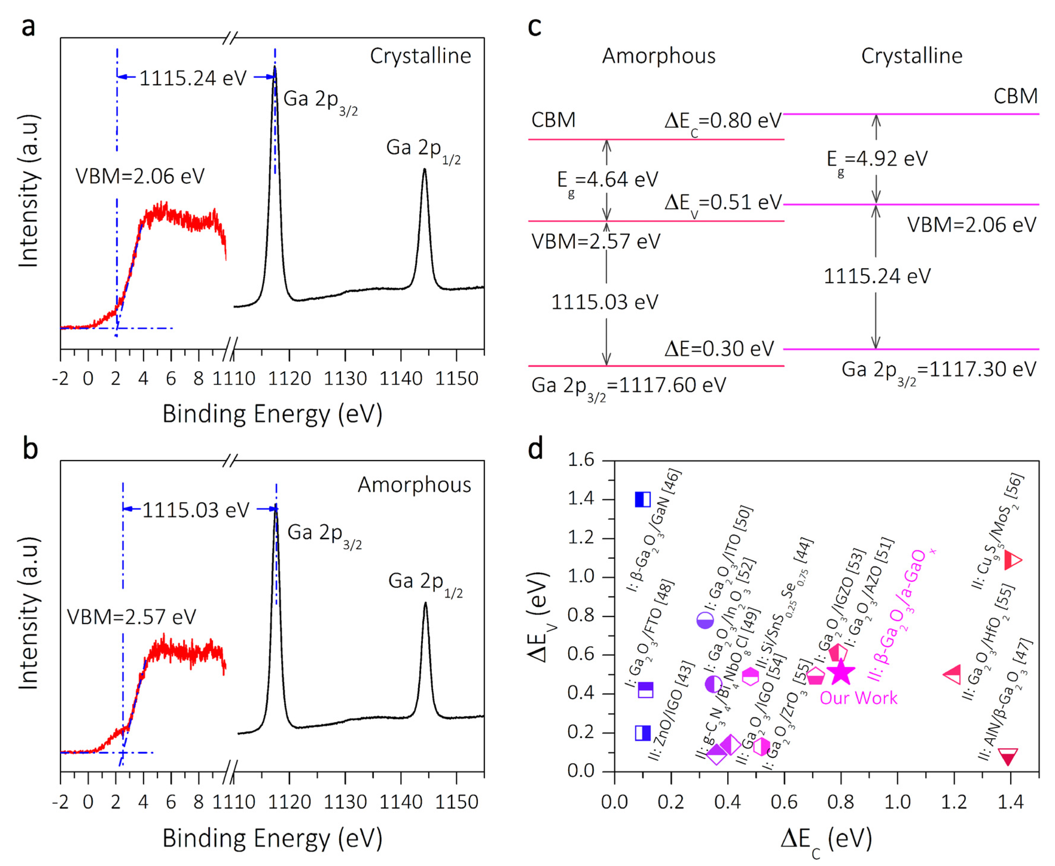
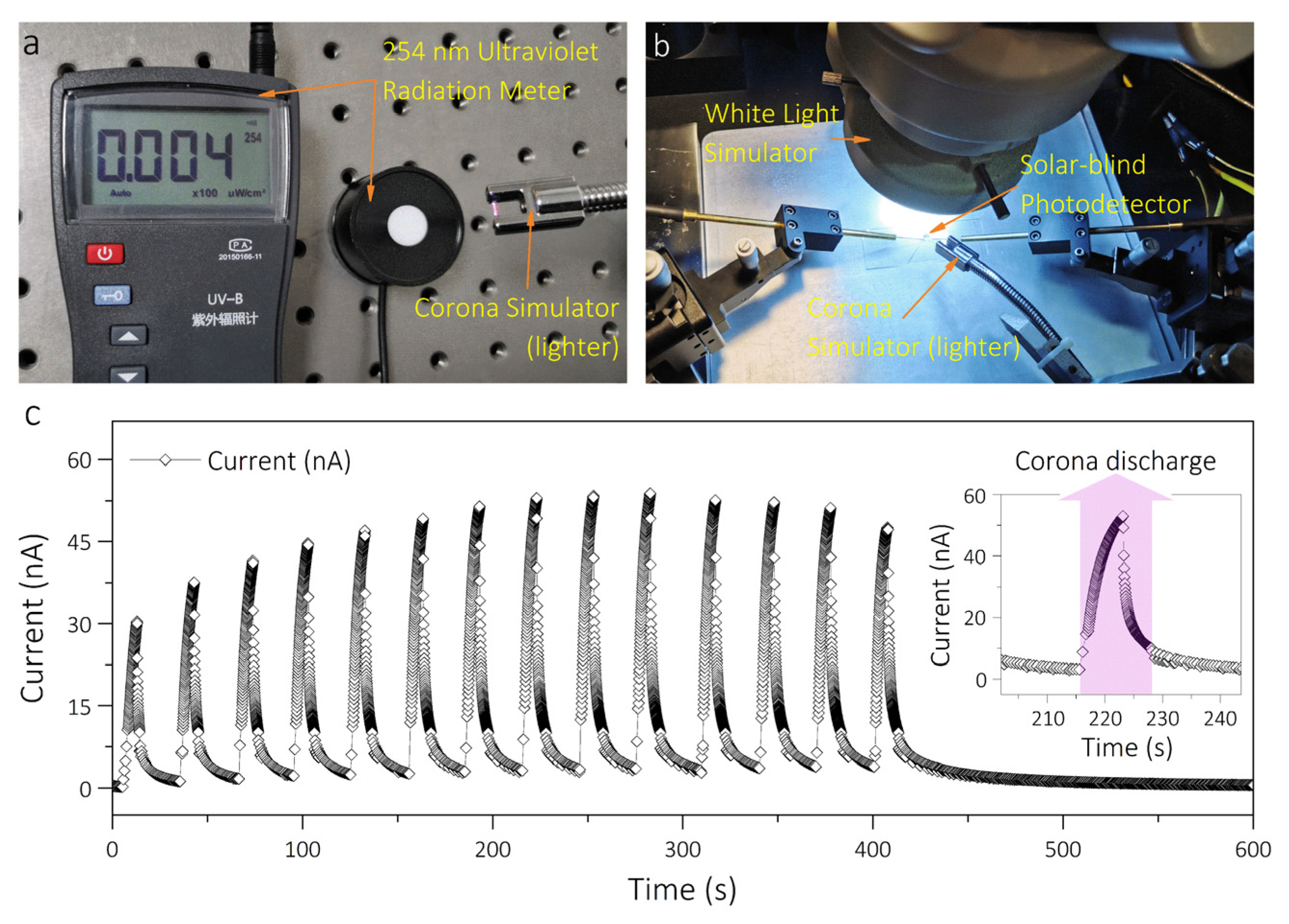
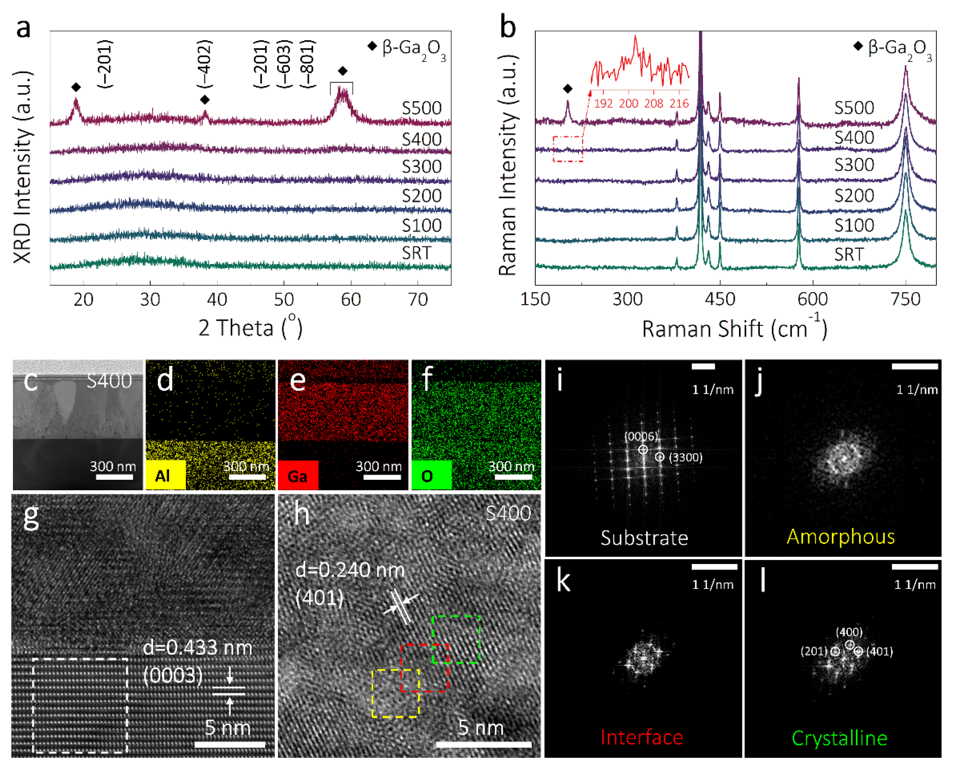
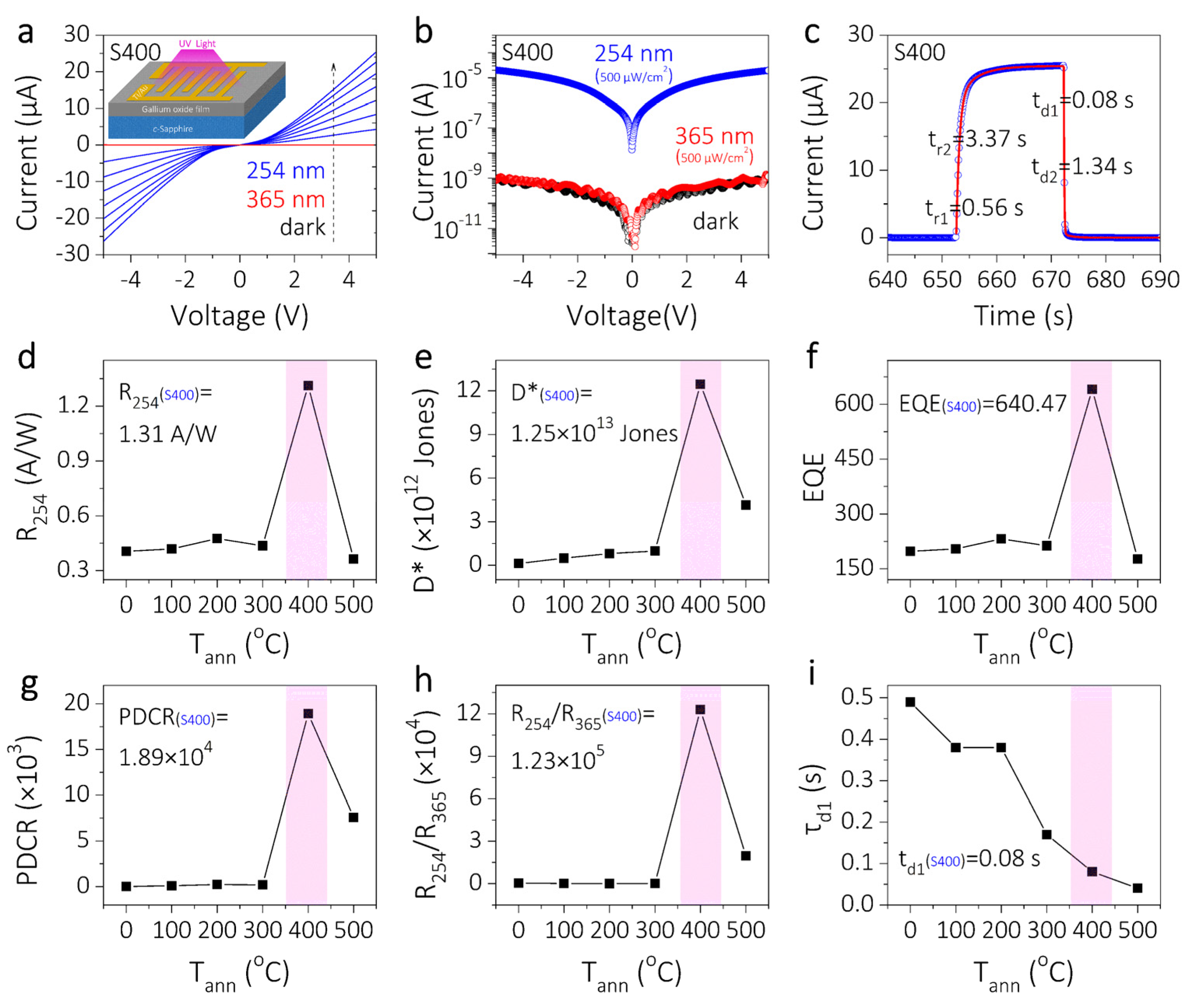
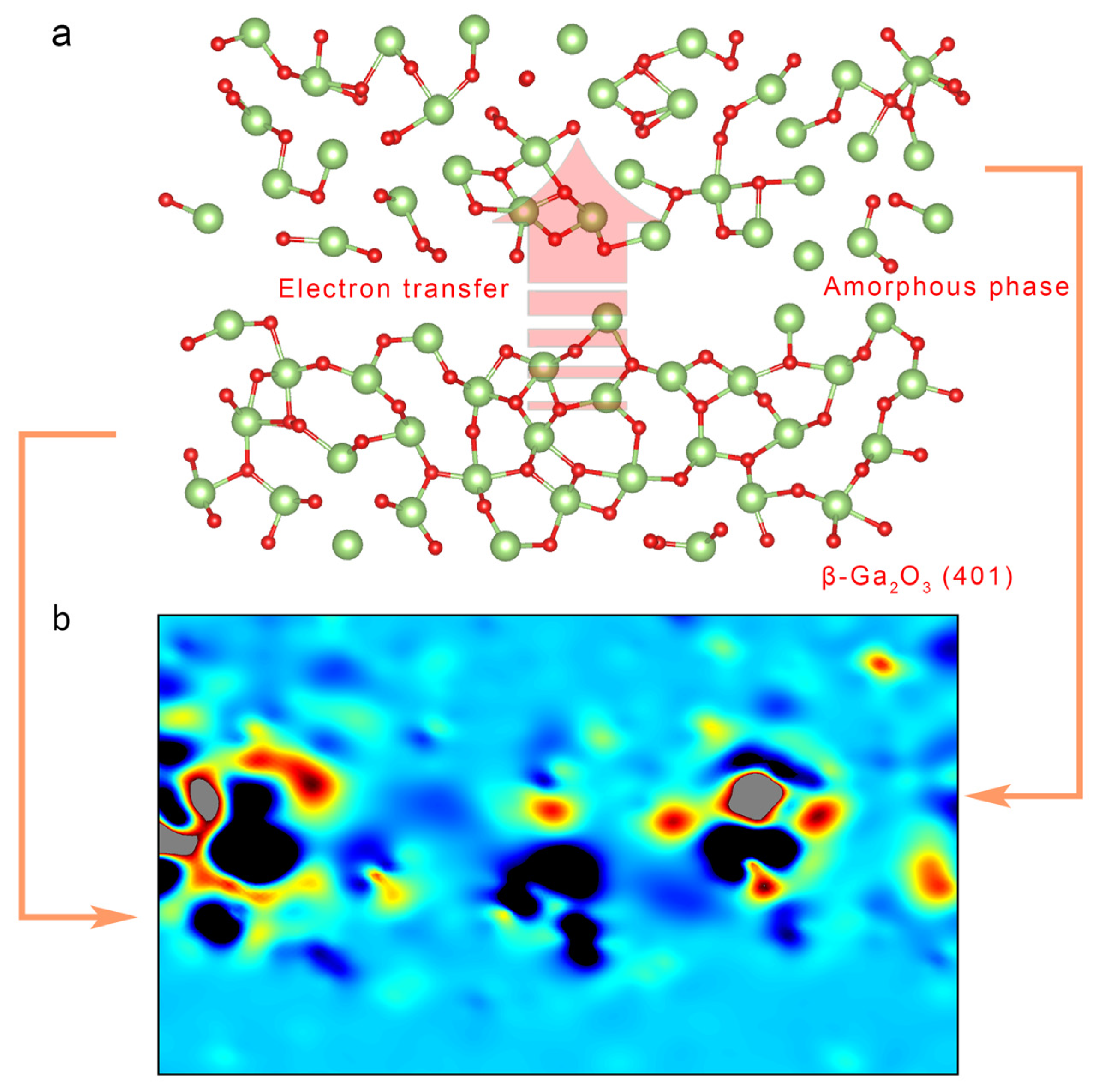
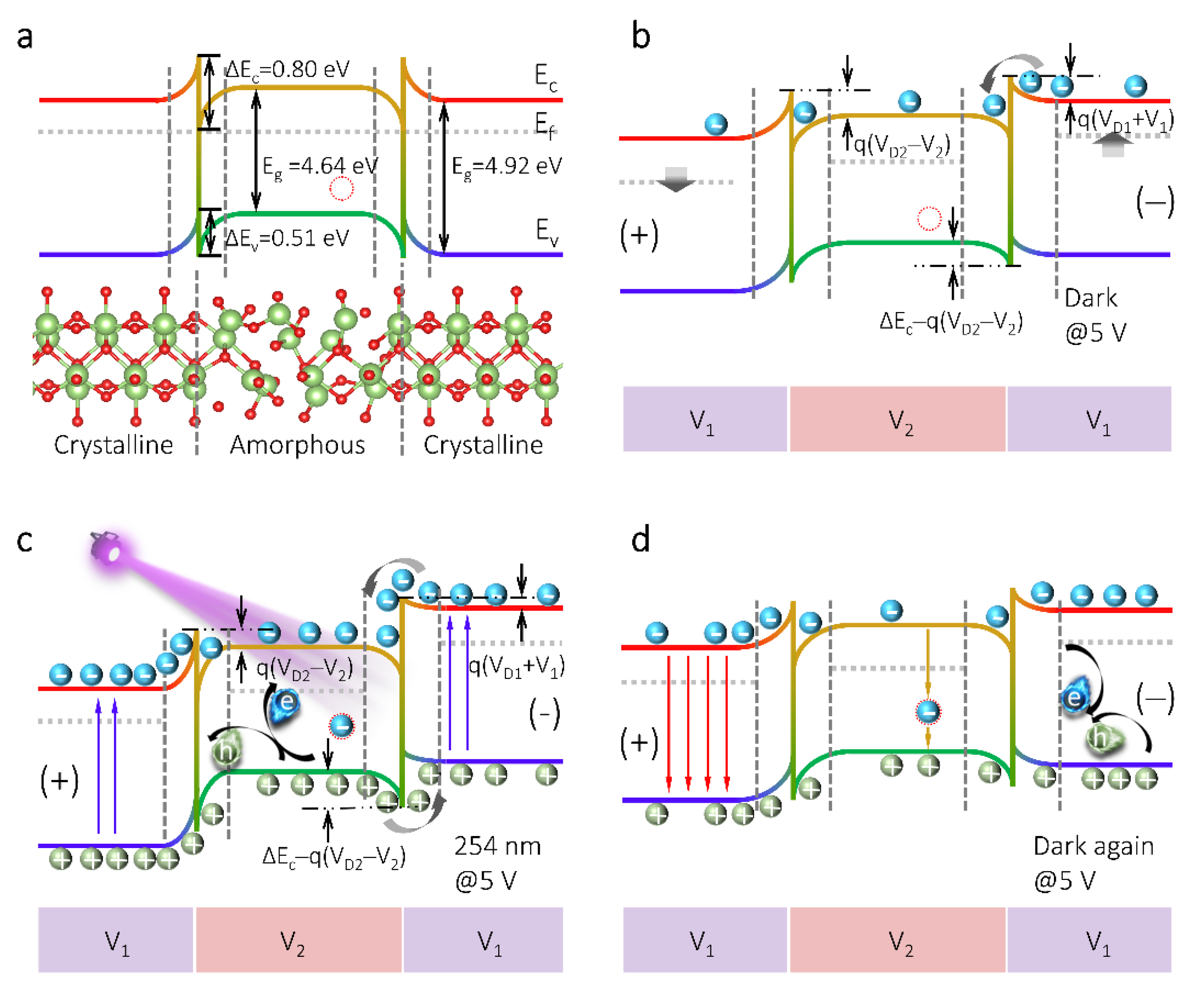
3. Results and Discussion

Figure 1a shows the XRD patterns of Ga2O3 films upon increasing the annealing temperature from RT to 500 °C. In the samples annealed between RT to 400 °C (SRT to S400), no signature peak was observed. However, regarding the sample annealed at 500 °C (S500), three distinct peaks were located near 18.40°, 37.90°, and 58.71°, corresponding to the ( 2 ¯ 01), ( 4 ¯ 02), and ( 6 ¯ 03) planes of monoclinic Ga2O3 (β-Ga2O3) (PDF#43-1012) [15]. Figure 1b presents the Raman scattering spectra of Ga2O3 films annealed at different temperatures. Similar to the XRD results, aside from the substrate-related vibration modes, no vibration mode was observed in SRT-S300. Meanwhile, in S500, a vibration mode located at ~201 cm−1 was observed, which originated from the vibration and translation of tetrahedron/vibration chain of β-Ga2O3 [36]. Hence, postannealing can promote the phase transition from amorphous to monoclinic Ga2O3, which is consistent with the results of previous reports [34]. Notably, a considerably weak vibration mode located at ~201 cm−1 was also observed in S400, indicating that S400 may have nanocrystals, that is, S400 may be a mixed-phase film constructed of amorphous and monoclinic Ga2O3.
To verify whether sample S400 was a mixed-phase film, cross-sectional high-resolution transmission electron microscopy (HRTEM) sample was prepared with a FEI Helios dual beam focused ion beam (FIB). Figure 1c shows the SEM image of the cross-section and the corresponding energy dispersive X-ray (EDX) elemental mapping images of Al (Figure 1d), Ga (Figure 1e), and O (Figure 1f), revealing that a film thickness of about ~490 nm, and Ga and O elements were uniformly distributed in the whole film with a clear interface structure. Further supporting evidence can be seen in the HRTEM image of the substrate with a zone axis of Al2O3 (1 1 ¯ 00) shown in Figure 1g [37], a lattice parameter of 0.432 nm corresponds to the (0003) plane of the c-plane sapphire substrate, and there is a clear abrupt interface between the film and sapphire substrate, and no obvious buffer or nucleation layer is observed. Figure 1i presents the fast Fourier transform (FFT) image corresponding to the white dotted selected area in Figure 1g, in which two sets of diffraction spots coming from the (0006) and (3300) plane of the substrate can be observed, indicating the highly ordered lattice array of the c-plane Al2O3 substrate. To investigate the amorphous and crystalline regions in the Ga2O3 films, high-angle annular dark-field (HAADF) HRTEM images of the sample S400 were taken. The amorphous/crystalline regions in the HRTEM image acquired from the S400 can be identified from the contrast (see Figure 1g,h). The yellow, red, and green dotted selected areas correspond to the amorphous, interface, and crystalline regions, respectively. In Figure 1h, the lattice parameter of the crystalline region was measured to be 0.24 nm, corresponding to the (401) plane of β-Ga2O3 [31]. Figure 1j–l represent the FFT images in Figure 1h. An observation can be made that the transition occurred from the diffraction ring (amorphous region) to the clear lattice (crystalline region), with the diffraction spots corresponding to the (201), (401), and (400) plane of β-Ga2O3. Figure S1 shows the HRTEM images of different regions of the S400. Obviously, there were randomly distributed crystalline phases Ga2O3 in different regions, indicating that the amorphous and crystalline phases were continuously distributed in sample S400. Therefore, sample S400 was clearly demonstrated to be a mixed-phase film, which consisted of amorphous domains and crystalline grains with random orientations.
To compare the solar-blind photoelectric characteristics of the mixed-phase Ga2O3 film (m-Ga2O3) and the others, the metal–semiconductor–metal (MSM) structured DUV PDs with Ti/Au interdigital electrodes (see inset of Figure 2a) were fabricated for photoresponse measurement, and the detailed procedure is provided in the Experimental Section. The I–V characteristics curves of Ga2O3 film PDs (SRT-S500) under dark, 365 nm, and 254 nm illumination (the light intensity of 254 nm is 100–700 μW/cm2, and the light intensity of 365 nm is 500 μW/cm2) are shown in Figure S2a–f. An observation can be made that the six devices could be considered as back-to-back Schottky barriers due to the apparently nonlinear I–V characteristics [38], and the photocurrent generated by PDs could be primarily determined by the number of photogenerated carriers under DUV light illumination [39]. As the light intensity increased from 100 to 700 μW/cm2, the photocurrent increased almost linearly, as shown in Figure S2g. Notably, m-Ga2O3 PD (S400) had the largest photocurrent under all ultraviolet light intensities, and the slope of the I–V characteristics curve of such device was also the largest, indicating that mixed-phase Ga2O3 PD had the strongest light dependence and internal gain. Figure S3 shows the dark current and photocurrent variation curves of Ga2O3 PDs, and an observation can be made that as the Ga2O3 film gradually crystallized, the dark current of the PD decreased continuously, and the decrease of the mixed-phase Ga2O3 PD was more significant. The aforementioned conclusions indicate that the mixed-phase Ga2O3 PD not only had a larger gain but also had a lower dark current. Figure 2a also shows the photocurrent variation of S400 with light intensity, and more detailed current changes under logarithmic coordinate at 254 nm, 365 nm, and dark conditions are shown in Figure 2b. As demonstrated in Supplementary Information (Note 2), main performance indexes such as responsivity (R), detectivity (D*), external quantum efficiency (EQE), photo-to-dark current ratio (PDCR), and rejection ratio (R254/R365) were calculated using corresponding equations, so as to further quantitatively compare the optoelectronic properties of the mixed-phase Ga2O3 PD and the other five devices. The calculation results of R, D*, EQE, PDCR, and R254/R365 of all six PDs under 5 V bias voltage and 500 μW/cm2 are shown in Figure 2d–h. As shown, the comprehensive performance of mixed-phase Ga2O3 PD was significantly superior compared with the other devices, with high responsivity (1.31 A/W), detectivity (1.35 × 10¹³ Jones), and external quantum efficiency (640.5%), in addition to significant photo-to-dark current ratio (2.20 × 10⁴) and rejection ratio (1.20 × 10⁵). The results demonstrated that the mixed-phase Ga2O3 can simultaneously improve the sensitivity and signal-to-noise ratio of the PD, which is more conducive to the application of the device in solar-blind DUV signal detection [2].
Figure S4 presents the time dependence of photoelectric properties of all six PDs with the switching of 254 nm light (500 mW/cm2) under the bias of 5 V. The photocurrent responded immediately as the light was turned on, revealing the instantaneous accumulation of photogenerated carriers [40]. Subsequently, the radiation transition and recombination tended to balance, thereby presenting a stationary photocurrent [39]. All PDs could be reversibly modulated by 254 nm illumination, and the photocurrent exhibited significant reproducibility even under continuous operation for 70 cycles. For a more detailed comparison of the photoresponses, the quantitative investigations were expressed by the fitting of the time-dependent photocurrent curves with a biexponential relaxation equation [41] (see Supplementary Information (Note 2)). The rise (τr) and decay times (τd) of all PDs were well fitted as shown in Figure S4. An observation can be made that the τr of all devices remained basically stable during the crystallization process of Ga2O3 films, but the τd gradually accelerated, particularly in S400 and S500. As shown in Figure 2c, the fast components of τr and τd of m-Ga2O3 PD (S400) were counted to be τr1 = 0.56 s and τd1 = 0.08 s, respectively. Among said components, the fast decay component (τd1) of S400 was significantly faster than the other amorphous devices (SRT-S300) and was considerably close to the value of the crystalline device (S500) (see Figure 2f). The comprehensive performance of the present mixed-phase Ga2O3 PD was significantly enhanced with not only high sensitivity and signal-to-noise ratio but also fast response, and the device also exhibited a more balanced performance in the reported results, as shown in Table 1.
To unravel the transport mechanism of enhanced performance in an amorphous/monoclinic mixed-phase Ga2O3 solar-blind photodetector, further research was conducted in combination with experimental and theoretical calculations. The interface between insulating oxide channels is considerably important, and the band offset at the edges of the conduction band and valence band largely determines the PD performance [51,52]. According to the method proposed by Kraut et al. [53], by extracting scanning data from the X-ray photoelectron spectroscopy (XPS), the band alignment of amorphous/monoclinic mixed-phase Ga2O3 can be obtained. Figure S5a shows a schematic diagram of the XPS test. An amorphous sample was first fully annealed at 900 °C to obtain a completely crystalline layer (crystalline Ga2O3), and then half-covered with a completely amorphous layer (amorphous Ga2O3). Figure 3a,b show the energy level of crystalline and amorphous Ga2O3. The valence band maximum (VBM)/Ga 2p3/2 values of crystalline and amorphous Ga2O3 were 2.06/1117.30 eV and 2.57/1117.60 eV, respectively. Additionally, to measure the absorption spectra of amorphous and crystalline samples, an ultraviolet–visible–infrared spectrophotometer was used (see Figure S5b for the schematic diagram), and the bandgaps of the amorphous and crystalline Ga2O3 films were calculated to be 4.64 eV and 4.92 eV, respectively. According to said values, the band offsets in valence band Δ E V and conduction band Δ E C were found to be 0.51 eV and 0.80 eV, respectively, and a more detailed description of amorphous/crystalline Ga2O3 band alignment calculation is described in Supplementary Information (Note 3). The band alignment schematic of the amorphous/crystalline interface are provided in Figure 3c, indicating that a typical staggered type-II band alignment was obtained, thereby potentially promoting the carriers transport by electric potential [51,54]. As shown in Figure 3d [51,52,54,55,56,57,58,59,60,61,62,63,64], the present mixed-phase Ga2O3 films had a large band offset including Δ E V and Δ E C compared with previous research. The band offset of m-Ga2O3 film in the present study completely meets the interface’s requirements for the driving force of separating electron–hole pairs.
DFT calculations were further performed to explore electronic characteristics of amorphous/crystalline mixed-phase Ga2O3. Based on the aforementioned TEM results, the (401) plane d-spacing was dominated. As such, an interface was constructed with crystalline β-Ga2O3 and amorphous Ga2O3 along (401), as shown in Figure 4a. During the relaxation process, several layers of Ga2O3 atoms near the interface were allowed to interact. To optimize the structure with cutoff energy of 500 eV, the Perdew–Berk–Ernzerhof (PBE) exchange correlation function was used. For the mixed-phase model, the Monkhorst–Pack k-point grid was set to 1 × 11 × 2, and the force threshold was set to 0.01 eV/Å. The energy convergence tolerance was 10−4 eV [65].
The difference in charge density perpendicular to the interface was explored, so as to understand the charge transfer and charge distribution between crystalline and amorphous phase Ga2O3 after the interface was formed. The difference in charge density is defined as [66]:
Δ ρ ( z ) = ρ m i x e d ρ c r y s t a l l i n e   ρ a m o r p h o u s
where ρ m i x e d , ρ c r y s t a l l i n e   , and ρ a m o r p h o u s are the charge density of mixed, crystalline, and amorphous phase Ga2O3, respectively. As shown in Figure 4b, the cyan and yellow regions represent the depletion and accumulation of charges in the space, respectively. Obviously, the charge transfers mainly occurred between the contact parts, which could lead to an effective separation of light generated carriers in this polarization field. The difference in charge indicates the charge transfer direction from the crystalline Ga2O3 to the amorphous Ga2O3 [67].
Figure 4a also shows a schematic diagram of light-induced carrier transfer in the mixed phase. The formation of said mixed phase will cause the redistribution of charges. The results show that the electrostatic intervention can make the amorphous phase negatively charged, while the crystal phase is positively charged. When two parts finally reach the same Fermi level, the built-in electric field from the crystalline phase to the amorphous phase will prevent the charge from diffusing [68,69]. Such a built-in electric field will act as a driving force to separate photogenerated carriers into different layers and can effectively prevent the recombination of photogenerated carriers. Through the separation of said carriers, the life of e-h+ can be effectively prolonged, and the overall performance will be promoted. Such theoretical calculation results agree with the aforementioned experimental analysis.
Based on the aforementioned results, the following mechanism is proposed to explain the enhanced performance of the mixed-phase Ga2O3 solar-blind photodetector, which is schematically introduced in Figure 5. The previous results show that the crystalline and amorphous domains in the mixed-phase Ga2O3 film (S400) are randomly distributed, and the mixed-phase structure presents a typical staggered type-II band alignment (see Figure 5a). To maintain the equilibrium of the mixed-phase interface Fermi level, the electrons in the crystalline Ga2O3 will migrate to the amorphous Ga2O3, thereby inducing the energy levels near the amorphous Ga2O3 bending upwards to form a built-in electric field (space charge region) around the interface. When two parts finally reach the same Ef, the built-in electric field from the crystalline phase to the amorphous one will prevent the further diffusion of charges [10,28].
The dark current transport process of mixed-phase Ga2O3 PD under a bias of 5 V is shown in Figure 5b. In general, a large number of oxygen vacancies acting as donor states in the amorphous Ga2O3 is beneficial for prolonging the life of electrons and inducing photoconductivity gain [10]. At the same time, a high density of oxygen vacancies has a high intrinsic carrier concentration [25], leading to lower resistivity and a large dark current of amorphous Ga2O3. However, the mixed-phase Ga2O3 PD exhibited a low dark current and can be explained as follows. Ga2O3 is a natural n-type oxide semiconductor material [2,3,70]. According to the traditional theory of nn heterojunction, the bias voltage applied to wide bandgap semiconductor is predominantly concentrated at the interface between different phase parts [28]. Since the crystalline and amorphous domains of mixed-phase Ga2O3 are considerably small, V1 and V2 are, respectively, approximated as the voltage applied to the interface between crystalline and amorphous domains. For defects such as oxygen vacancies, the resistivity of amorphous domains is smaller than that of crystalline domains, such that the voltage V1 added on crystalline domains is higher than the voltage V2 added on amorphous domains. Thus, the heights of the two barriers for electrons and one barrier for holes are q(VD1 + V1), q(VD2 − V2) and Δ E C q(VD2 − V2), respectively. Thereinto, qVD1 and qVD2 are the barrier heights of electrons and holes without bias voltage, and Δ E C is the conduction band offset. The transfer of most electrons is blocked due to the presence of a high-density barrier layer at the interface between Ga2O3 domains of different phases, which is primarily responsible for the low dark current of the present mixed-phase Ga2O3 PD.
Figure 5c displays a schematic illustration of solar-blind ultraviolet light on the amorphous/crystal interface. The high-energy light will stimulate the m-Ga2O3 film to rapidly excite many electrons into the conduction band and leave holes in the valence band of both amorphous and crystalline Ga2O3. Hence, the resistance of both Ga2O3 domains will decrease. However, because of the higher defect concentration of amorphous domains, the resistivity thereof is lower than that of the crystalline. Compared with the amorphous Ga2O3, the photogenerated carriers caused the resistivity of the crystalline domains to decrease more [71], such that V2 increased to be larger than V1. After that, the two barriers of electrons at the interface were lowered, which promoted the transport of photogenerated electrons. On the contrary, the barriers of holes were raised, meaning that the photocurrent was mainly composed of electrons [72]. As such, the mixed-phase based PD exhibited a photocurrent much higher than the dark current. Furthermore, according to the previous results, the photocurrent of mixed-phase based PD was significantly greater than that of other five devices, which is usually related to the effective separation and prolonged lifetime of carriers [22]. The present experimental and theoretical results all reveal that the charge transfer mainly occurred in the mixed phase interface, potentially leading to the effective separation of light-induced carriers under such polarization field. Moreover, the Δ E V and   Δ E C at the amorphous/crystal interface were 0.5 and 0.8 eV, respectively, and the mixed phase interface presented a type II band alignment. Such band offset will act as a driving force to separate photogenerated carriers into different layers, which is a key mechanism that can restrain recombination processes and extend the life of light-induced carriers, resulting in a significant enhancement in photocurrent. In fact, an assumption can be made that such mechanism will exist in all devices with crystalline/amorphous interfaces. However, as the thin film gradually crystallized, the number of crystalline/amorphous interfaces first increased and then decreased, and the presence of continuous amorphous (S100–S300) or crystalline (S500) may also affect such mechanism. Ultimately, the best crystalline/amorphous interface arrangement was obtained in S400, which may be the reason for S400 having the best performance. In addition, since many oxygen vacancies in amorphous Ga2O3 act as electron traps [18,25], when UV illumination was turned on, the photogenerated electrons were captured by the oxygen vacancies. Hence, the life of electrons can be effectively prolonged, promoting enhancement of the photocurrent. Finally, the mixed-phase Ga2O3 PD had the highest photocurrent and enhanced performance by effectively separating photogenerated carriers and prolonging the lifetime thereof.
Figure 5d shows that when the ultraviolet light was turned off, the photogenerated electron–hole pairs recombined rapidly. In general, the amorphous domain could trap electrons and induce gain, in addition to slowing down the recombination of electrons in the device. However, the present mixed-phase solar-blind PD still achieved rapid decay time due to the rapidly established barrier at the mixed-phase interface.
Corona discharge detection is an important application for solar-blind ultraviolet photodetectors [4]. Owing to the existence of weak solar-blind signals in the exposed high-voltage cables and components, the Ga2O3 based photodetector can be placed further away from the arc for long-distance and wide-angle detection if stable and highly sensitive detection can be achieved. In order to explore the corona discharge detection capability of m-Ga2O3 PD, a simple corona discharge test system was constructed, as shown in Figure 6. Figure 6a shows the photograph of the intensity test of the ~254 nm deep ultraviolet light generated by the corona simulator (lighter). The radiometer shows that the intensity was only 0.4 μW/cm2. As shown in Figure 6b, the corona detection environment was simulated under sunlight, and the photoresponse of m-Ga2O3 PD is shown in Figure 6c. When the lighter was discharged, the device responded repeatedly with a photocurrent signal of about 30~50 nA. Such result indicates that the solar-blind ultraviolet photodetector based on m-Ga2O3 film had significant sensitivity and has potential applications in high-voltage corona discharge and other fields.

4. Conclusions

In summary, simultaneously enhanced sensitivity and signal-to-noise ratio of MSM solar-blind DUV PD based on an amorphous/monoclinic homogeneous mixed-phase structure Ga2O3 film was reported, and the transport mechanism was discussed in detail. The present mixed-phase Ga2O3 solar-blind DUV PD exhibited a high R of 1.31 A/W, D* of 1.35 × 10¹³ Jones, and EQE of 640.5%, in addition to significant PDCR of 2.20 × 10⁴ and rejection ratio (R254 nm/R365 nm) of 1.20 × 10⁵, thereby demonstrating high sensitivity and signal-to-noise ratio of the PD. Additionally, a fast recovery speed of 80 ms was achieved, which is significantly faster than other amorphous devices, and is considerably close to the value of the crystalline device. In combination with experimental and theoretical investigations, the results of the present study demonstrate that the band offset and barrier height difference of the mixed-phase interface were responsible for enhancing the comprehensive performance of Ga2O3 solar-blind DUV PDs. Moreover, based on the mixed-phase Ga2O3 PD, the potential application in the detection of high-voltage corona discharge was explored, and a clear and stable corona discharge detection signal was obtained. The present findings may contribute to a better understanding of the enhanced performance in the mixed-phase DUV photoelectronic devices and provide an efficient approach for promoting comprehensive performance in future solar-blind detection applications.

Supplementary Materials

The following are available online at https://www.mdpi.com/article/10.3390/cryst11091111/s1. See the supplementary material for detailed information on the HRTEM images of the mixed-phase Ga2O3 (Figure S1), the I–V characteristics curve (Figure S2), dark current and photocurrent variation curves (Figure S3) and transient response (Figure S4) of Ga2O3 PDs, determination of bandgap of Ga2O3 films (Figure S5), the deposition of the Ga2O3 thin films (Note 1), the main performance index calculations of PDs (Note 2), and the band alignment calculation of the mixed-phase Ga2O3 (Note 3).

Author Contributions

Conceptualization, W.L.; methodology, H.L. (Haowen Liu), S.Z., Y.X.; software, H.L. (Honglin Li); formal analysis, W.L., H.L. (Haowen Liu), H.L. (Honglin Li), S.Z.; investigation, H.L. (Haowen Liu), H.L. (Honglin Li), W.L., S.Z., H.Z., L.Y., Y.X.; resources, S.F., Y.C., C.K.; data curation, H.L. (Haowen Liu), H.L. (Honglin Li), Y.X.; writing—original draft preparation, H.L. (Haowen Liu), H.L. (Honglin Li); writing—review and editing, W.L., L.Y., Y.X.; supervision, W.L., Y.C., C.K., L.Y.; project administration, W.L.; funding acquisition, W.L., H.Z., L.Y. All authors have read and agreed to the published version of the manuscript.

Funding

This research received no external funding.

Institutional Review Board Statement

Not applicable.

Informed Consent Statement

Not applicable.

Data Availability Statement

The data that support the findings of this study are available from the corresponding author upon reasonable request.

Acknowledgments

The authors gratefully acknowledge support from the National Natural Science Foundation of China (Grant Nos. 11904041 and 51472038), the Natural Science Foundation of Chongqing (Grant Nos. cstc2020jcyj-msxmX0557, cstc2020jcyj-msxmX0533 and cstc2019jcyj-msxmX0237) and the Science and Technology Research Project of Chongqing Education Committee (Grant Nos. KJQN201900542, KJQN202000511 and KJQN201800501).

Conflicts of Interest

The authors declare no conflict of interest.

References

  1. Pearton, S.J.; Yang, J.; Cary, P.H.; Ren, F.; Kim, J.; Tadjer, M.J.; Mastro, M.A. A review of Ga2O3 materials, processing, and devices. Appl. Phys. Rev. 2018, 5, 011301. [Google Scholar] [CrossRef] [Green Version]
  2. Xu, J.; Zheng, W.; Huang, F. Gallium Oxide Solar-Blind Ultraviolet Photodetector: A Review. J. Mater. Chem. C 2019, 7, 8753–8770. [Google Scholar] [CrossRef]
  3. Xie, C.; Lu, X.; Tong, X.; Zhang, Z.; Liang, F.; Liang, L.; Luo, L.; Wu, Y. Recent Progress in Solar-Blind Deep-Ultraviolet Photodetectors Based on Inorganic Ultrawide Bandgap Semiconductors. Adv. Funct. Mater. 2019, 29, 1806006. [Google Scholar] [CrossRef]
  4. Chen, X.; Ren, F.; Gu, S.; Ye, J. Review of gallium-oxide-based solar-blind ultraviolet photodetectors. Photonics Res. 2019, 7, 381–415. [Google Scholar] [CrossRef]
  5. Hou, X.H.; Zou, Y.N.; Ding, M.F.; Qin, Y.; Zhang, Z.F.; Ma, X.L.; Tan, P.J.; Yu, S.J.; Zhou, X.Z.; Zhao, X.L.; et al. Review of polymorphous Ga2O3 materials and their solar-blind photodetector applications. J. Phys. D Appl. Phys. 2021, 54, 043001. [Google Scholar] [CrossRef]
  6. Liang, H.L.; Han, Z.Y.; Mei, Z.X. Recent Progress of Deep Ultraviolet Photodetectors using Amorphous Gallium Oxide Thin Films. Phys. Status Solidi A 2021, 218, 2000339. [Google Scholar] [CrossRef]
  7. Monroy, E.; Omnès, F.; Calle, F. Wide-bandgap semiconductor ultraviolet photodetectors. Semicond. Sci. Technol. 2003, 18, R33–R51. [Google Scholar] [CrossRef]
  8. Qin, Y.; Li, L.; Zhao, X.; Tompa, G.S.; Dong, H.; Jian, G.; He, Q.M.; Tan, P.; Hou, X.; Zhang, Z.; et al. Metal-Semiconductor-Metal ε-Ga2O3 Solar-Blind Photodetectors with a Record-High Responsivity Rejection Ratio and Their Gain Mechanism. ACS Photonics 2020, 7, 812–820. [Google Scholar] [CrossRef]
  9. Zhang, H.C.; Liang, F.Z.; Song, K.; Xing, C.; Wang, D.H.; Yu, H.B.; Huang, C.; Sun, Y.; Yang, L.; Zhao, X.L.; et al. Demonstration of AlGaN/GaN-based ultraviolet phototransistor with a record high responsivity over 3.6 × 10⁷ A/W. Appl. Phys. Lett. 2021, 118, 242105. [Google Scholar] [CrossRef]
  10. Fan, M.M.; Liu, K.W.; Chen, X.; Wang, X.; Zhang, Z.Z.; Li, B.H.; Shen, D.Z. Mechanism of Excellent Photoelectric Characteristics in Mixed-Phase ZnMgO Ultraviolet Photodetectors with Single Cutoff Wavelength. ACS Appl. Mater. Interfaces 2015, 7, 20600–20606. [Google Scholar] [CrossRef]
  11. Chen, Y.; Lu, Y.; Lin, C.; Tian, Y.; Gao, C.; Dong, L.; Shan, C. Self-powered diamond/β-Ga2O3 photodetectors for solar-blind imaging. J. Mater. Chem. C 2018, 6, 5727–5732. [Google Scholar] [CrossRef]
  12. Chikoidze, E.; Tchelidze, T.; Sartel, C.; Chi, Z.; Kabouche, R.; Madaci, I.; Rubio, C.; Mohamed, H.; Sallet, V.; Medjdoub, F.; et al. Ultra-high critical electric field of 13.2 MV/cm for Zn-doped p-type β-Ga2O3. Mater. Today Phys. 2020, 15, 100263. [Google Scholar] [CrossRef]
  13. Feng, W.; Wang, X.N.; Zhang, J.; Wang, L.F.; Zheng, W.; Hu, P.A.; Cao, W.W.; Yang, B. Synthesis of two-dimensional β-Ga2O3 nanosheets for high-performance solar blind photodetectors. J. Mater. Chem. C 2014, 2, 3254–3259. [Google Scholar] [CrossRef]
  14. Zhang, D.; Zheng, W.; Lin, R.C.; Li, T.T.; Zhang, Z.J.; Huang, F. High quality β-Ga2O3 film grown with N2O for high sensitivity solar-blind-ultraviolet photodetector with fast response speed. J. Alloys Compd. 2018, 735, 150–154. [Google Scholar] [CrossRef]
  15. Zhang, M.M.; Kang, S.; Zhang, K.; Wu, Y.T.; Feng, S.L.; Lu, W.Q. Facile Synthesis of β-Ga2O3 nanowires network for solar-blind ultraviolet photodetector. J. Phys. D: Appl. Phys. 2021, 54, 175106. [Google Scholar] [CrossRef]
  16. Hou, X.H.; Sun, H.D.; Long, S.B.; Tompa, G.S.; Salagaj, T.; Qin, Y.; Zhang, Z.F.; Tan, P.J.; Yu, S.J.; Liu, M. Ultrahigh-Performance Solar-Blind Photodetector Based on α-Phase-Dominated Ga2O3 Film With Record Low Dark Current of 81 fA. IEEE Electron. Device Lett. 2019, 40, 1483–1486. [Google Scholar] [CrossRef]
  17. Wu, C.; He, C.; Guo, D.; Zhang, F.; Li, P.; Wang, S.; Liu, A.; Wu, F.; Tang, W. Vertical α/β-Ga2O3 phase junction nanorods array with graphene-silver nanowire hybrid conductive electrode for high-performance self-powered solar-blind photodetectors. Mater. Today Phys. 2020, 12, 100193. [Google Scholar] [CrossRef]
  18. Cui, S.; Mei, Z.; Zhang, Y.; Liang, H.; Du, X. Room-Temperature Fabricated Amorphous Ga2O3 High-Response-Speed Solar-Blind Photodetector on Rigid and Flexible Substrates. Adv. Opt. Mater. 2017, 5, 1700454. [Google Scholar] [CrossRef]
  19. Teng, Y.; Song le, X.; Ponchel, A.; Yang, Z.K.; Xia, J. Self-assembled metastable gamma-Ga2O3 nanoflowers with hexagonal nanopetals for solar-blind photodetection. Adv. Mater. 2014, 26, 6238–6243. [Google Scholar] [CrossRef]
  20. Kong, W.Y.; Wu, G.A.; Wang, K.Y.; Zhang, T.F.; Zou, Y.F.; Wang, D.D.; Luo, L.B. Graphene-β-Ga2O3 Heterojunction for Highly Sensitive Deep UV Photodetector Application. Adv. Mater. 2016, 28, 10725–10731. [Google Scholar] [CrossRef] [PubMed]
  21. Oshima, T.; Okuno, T.; Arai, N.; Suzuki, N.; Ohira, S.; Fujita, S. Vertical Solar-Blind Deep-Ultraviolet Schottky Photodetectors Based on β-Ga2O3 Substrates. Appl. Phys. Express 2008, 1, 011202. [Google Scholar] [CrossRef]
  22. Li, Y.; Tokizono, T.; Liao, M.; Zhong, M.; Koide, Y.; Yamada, I.; Delaunay, J.J. Effi cient Assembly of Bridged β-Ga2O3 Nanowires for Solar-Blind Photodetection. Adv. Funct. Mater. 2010, 20, 3972–3978. [Google Scholar] [CrossRef]
  23. Wang, D.H.; Liu, X.; Fang, S.; Huang, C.; Kang, Y.; Yu, H.B.; Liu, Z.L.; Zhang, H.C.; Long, R.; Xiong, Y.J.; et al. Pt/AlGaN Nanoarchitecture: Toward High Responsivity, Self-Powered Ultraviolet-Sensitive Photodetection. Nano Lett. 2020, 21, 120–129. [Google Scholar] [CrossRef] [PubMed]
  24. Gong, H.H.; Yu, X.X.; Xu, Y.; Chen, X.H.; Kuang, Y.; Lv, Y.J.; Yang, Y.; Ren, F.F.; Feng, Z.H.; Gu, S.L.; et al. β-Ga2O3 vertical heterojunction barrier Schottky diodes terminated with p-NiO field limiting rings. Appl. Phys. Lett. 2021, 118, 202102. [Google Scholar] [CrossRef]
  25. Qian, L.; Wu, Z.; Zhang, Y.; Lai, P.; Liu, X.; Li, Y. Ultrahigh-Responsivity, Rapid-Recovery, Solar-Blind Photodetector Based on Highly Nonstoichiometric Amorphous Gallium Oxide. ACS Photonics 2017, 4, 2203–2211. [Google Scholar] [CrossRef]
  26. Wong, M.H.; Murakami, H.; Kumagai, Y.; Higashiwaki, M. Aperture-limited conduction and its possible mechanism in ion-implanted current aperture vertical β-Ga2O3 MOSFETs. Appl. Phys. Lett. 2021, 118, 012102. [Google Scholar] [CrossRef]
  27. Mukhopadhyay, P.; Schoenfeld, W.V. Tin Gallium Oxide Solar-Blind Photodetectors on Sapphire Grown by Molecular Beam Epitaxy. Appl. Opt. 2019, 58, D22–D27. [Google Scholar] [CrossRef] [PubMed]
  28. Han, S.; Hu, S.R.; Cao, P.J.; Liu, W.J.; Zeng, Y.X.; Jia, F.; Xu, W.Y.; Liu, X.K.; Zhu, D.L.; Lu, Y.M. High signal/noise ratio deep UV detector with maximum response at 230 nm based on mix-phase MgZnO deposited under high laser energy condition. Europhys. Lett. 2018, 124, 18006. [Google Scholar] [CrossRef]
  29. Fan, M.M.; Liu, K.W.; Zhang, Z.Z.; Li, B.H.; Chen, X.; Zhao, D.X.; Shan, C.X.; Shen, D.Z. High-performance solar-blind ultraviolet photodetector based on mixed-phase ZnMgO thin film. Appl. Phys. Lett. 2014, 105, 011117. [Google Scholar] [CrossRef] [Green Version]
  30. Lee, S.H.; Kim, S.B.; Moon, Y.-J.; Kim, S.M.; Jung, H.J.; Seo, M.S.; Lee, K.M.; Kim, S.-K.; Lee, S.W. High-Responsivity Deep-Ultraviolet-Selective Photodetectors Using Ultrathin Gallium Oxide Films. ACS Photonics 2017, 4, 2937–2943. [Google Scholar] [CrossRef]
  31. Sun, H.L.; Zhang, L.Y.; Yu, J.Y.; Wang, S.L.; Guo, D.Y.; Li, C.R.; Wu, F.M.; Liu, A.P.; Li, P.G.; Tang, W.H. Phase junction enhanced photocatalytic activity of Ga2O3 nanorod arrays on flexible glass fiber fabric. RSC Adv. 2020, 10, 11499–11506. [Google Scholar] [CrossRef] [Green Version]
  32. Wang, X.; Xu, Q.; Li, M.; Shen, S.; Wang, X.; Wang, Y.; Feng, Z.; Shi, J.; Han, H.; Li, C. Photocatalytic Overall Water Splitting Promoted by an α-β phase Junction on Ga2O3. Angew. Chem. Int. Ed. 2012, 51, 13089–13092. [Google Scholar] [CrossRef]
  33. Lu, Y.M.; Li, C.; Chen, X.H.; Han, S.; Cao, P.J.; Jia, F.; Zeng, Y.X.; Liu, X.K.; Xu, W.Y.; Liu, W.J.; et al. Preparation of Ga2O3 thin film solar-blind photodetectors based on mixed-phase structure by pulsed laser deposition. Chin. Phys. B 2019, 28, 018504. [Google Scholar] [CrossRef]
  34. Kumar, S.S.; Rubio, E.J.; Noor-A-Alam, M.; Martinez, G.; Manandhar, S.; Shutthanandan, V.; Thevuthasan, S.; Ramana, C.V. Structure, Morphology, and Optical Properties of Amorphous and Nanocrystalline Gallium Oxide Thin Films. J. Phys. Chem. C 2013, 117, 4194–4200. [Google Scholar] [CrossRef]
  35. Wang, Y.H.; Cui, W.J.; Yu, J.; Zhi, Y.S.; Li, H.R.; Hu, Z.Y.; Sang, X.H.; Guo, E.J.; Tang, W.H.; Wu, Z.P. One-Step Growth of Amorphous/Crystalline Ga2O3 Phase-Junctions for High-Performance Solar-Blind Photodetection. ACS Appl. Mater. Interfaces 2019, 11, 45922–45929. [Google Scholar] [CrossRef]
  36. Kranert, C.; Sturm, C.; Schmidt-Grund, R.; Grundmann, M. Raman tensor elements of β-Ga2O3. Sci. Rep. 2016, 6, 35964. [Google Scholar] [CrossRef]
  37. Du, J.L.; Fang, Y.; Fu, E.G.; Ding, X.; Yu, K.Y.; Wang, Y.G.; Wang, Y.Q.; Baldwin, J.K.; Wang, P.P.; Bai, Q. What determines the interfacial configuration of Nb/Al2O3 and Nb/MgO interface. Sci. Rep. 2016, 6, 33931. [Google Scholar] [CrossRef] [PubMed]
  38. Mohamed, M.; Irmscher, K.; Janowitz, C.; Galazka, Z.; Manzke, R.; Fornari, R. Schottky barrier height of Au on the transparent semiconducting oxide β-Ga2O3. Appl. Phys. Lett. 2012, 101, 132106. [Google Scholar] [CrossRef]
  39. Xu, X.; Chen, J.; Cai, S.; Long, Z.; Zhang, Y.; Su, L.; He, S.; Tang, C.; Liu, P.; Peng, H.; et al. A Real-Time Wearable UV-Radiation Monitor based on a High-Performance p-CuZnS/n-TiO2 Photodetector. Adv. Mater. 2018, 30, 1803165. [Google Scholar] [CrossRef] [PubMed]
  40. Oh, S.; Kim, C.-K.; Kim, J. High Responsivity β-Ga2O3 Metal-Semiconductor-Metal Solar-Blind Photodetectors with Ultraviolet Transparent Graphene Electrodes. ACS Photonics 2017, 5, 1123–1128. [Google Scholar] [CrossRef]
  41. Guo, P.; Xiong, J.; Zhao, X.H.; Sheng, T.; Yue, C.; Tao, B.W.; Liu, X.Z. Growth characteristics and device properties of MOD derived β-Ga2O3 films. J. Mater. Sci. Mater. Electron. 2014, 25, 3629–3632. [Google Scholar] [CrossRef]
  42. Zhuo, R.R.; Wu, D.; Wang, Y.G.; Wu, E.P.; Jia, C.; Shi, Z.F.; Xu, T.T.; Tian, Y.T.; Li, X.J. A self-powered solar-blind photodetector based on a MoS2/β-Ga2O3 heterojunction. J. Mater. Chem. C 2018, 6, 10982–10986. [Google Scholar] [CrossRef]
  43. Zhao, B.; Wang, F.; Chen, H.; Zheng, L.; Su, L.; Zhao, D.; Fang, X. An Ultrahigh Responsivity (9.7 mA W−1) Self-Powered Solar-Blind Photodetector Based on Individual ZnO-Ga2O3 Heterostructures. Adv. Funct. Mater. 2017, 27, 1700264. [Google Scholar] [CrossRef]
  44. Wu, Z.P.; Jiao, L.; Wang, X.L.; Guo, D.Y.; Li, W.H.; Li, L.H.; Huang, F.; Tang, W.H. A self-powered deep-ultraviolet photodetector based on an epitaxial Ga2O3/Ga: ZnO heterojunction. J. Mater. Chem. C 2017, 5, 8688–8693. [Google Scholar] [CrossRef]
  45. Cai, J.; Xu, X.J.; Su, L.X.; Yang, W.; Chen, H.Y.; Zhang, Y.; Fang, X.S. Self-Powered n-SnO2/p-CuZnS Core-Shell Microwire UV Photodetector with Optimized Performance. Adv. Opt. Mater. 2018, 6, 1800213. [Google Scholar] [CrossRef]
  46. Guo, D.; Su, Y.; Shi, H.; Li, P.; Zhao, N.; Ye, J.; Wang, S.; Liu, A.; Chen, Z.; Li, C.; et al. Self-Powered Ultraviolet Photodetector with Superhigh Photoresponsivity (3.05 A/W) Based on the GaN/Sn: Ga2O3 pn Junction. ACS Nano 2018, 12, 12827–12835. [Google Scholar] [CrossRef]
  47. Li, S.; Guo, D.; Li, P.G.; Wang, X.; Wang, Y.; Yan, Z.; Liu, Z.; Zhi, Y.; Huang, Y.; Wu, Z.; et al. Ultrasensitive, Superhigh Signal-to-Noise Ratio, Self-Powered Solar-Blind Photodetector Based on n-Ga2O3/p-CuSCN Core-Shell Microwire Heterojunction. ACS Appl. Mater. Interfaces 2019, 11, 35105–35114. [Google Scholar] [CrossRef] [PubMed]
  48. Zheng, W.; Lin, R.C.; Ran, J.X.; Zhang, Z.J.; Ji, X.; Huang, F. Vacuum-Ultraviolet Photovoltaic Detector. ACS Nano 2018, 12, 425–431. [Google Scholar] [CrossRef] [PubMed]
  49. Xu, X.; Hu, J.; Yin, Z.; Xu, C. Photoanode current of large-area MoS2 ultrathin nanosheets with vertically mesh-shaped structure on indium tin oxide. ACS Appl. Mater. Interfaces 2014, 6, 5983–5987. [Google Scholar] [CrossRef] [PubMed]
  50. Arora, K.; Goel, N.; Kumar, M.; Kumar, M. Ultrahigh Performance of Self-Powered β-Ga2O3 Thin Film Solar-Blind Photodetector Grown on Cost-Effective Si Substrate Using High-Temperature Seed Layer. ACS Photonics 2018, 5, 2391–2401. [Google Scholar] [CrossRef]
  51. Wheeler, V.D.; Shahin, D.I.; Tadjer, M.J.; Eddy, C.R., Jr. Band alignments of atomic layer deposited ZrO2 and HfO2 high-k dielectrics with (-201) β-Ga2O3. ECS J. Solid State Sci. Technol. 2016, 6, Q3052–Q3055. [Google Scholar] [CrossRef]
  52. Carey, P.H., IV; Ren, F.; Hays, D.C.; Gila, B.; Pearton, S.; Jang, S.; Kuramata, A. Band offsets in ITO/Ga2O3 heterostructures. Appl. Surf. Sci. 2017, 422, 179–183. [Google Scholar] [CrossRef] [Green Version]
  53. Kraut, E.A.; Grant, R.W.; Waldrop, J.R.; Kowalczyk, S.P. Precise Determination of the Valence-Band Edge in X-Ray Photoemission Spectra: Application to Measurement of Semiconductor Interface Potentials. Phys. Rev. Lett. 1980, 44, 1620–1623. [Google Scholar] [CrossRef]
  54. Seul, H.J.; Kim, M.J.; Yang, H.J.; Cho, M.H.; Cho, M.H.; Song, W.B.; Jeong, J.K. Atomic Layer Deposition Process-Enabled Carrier Mobility Boosting in Field-Effect Transistors through a Nanoscale ZnO/IGO Heterojunction. ACS Appl. Mater. Interfaces 2020, 12, 33887–33898. [Google Scholar] [CrossRef]
  55. Gao, W.; Zheng, Z.; Huang, L.; Yao, J.; Zhao, Y.; Xiao, Y.; Li, J. Self-Powered SnS1-xSex Alloy/Silicon Heterojunction Photodetectors with High Sensitivity in a Wide Spectral Range. ACS Appl. Mater. Interfaces 2019, 11, 40222–40231. [Google Scholar] [CrossRef]
  56. Kalra, A.; Vura, S.; Rathkanthiwar, S.; Muralidharan, R.; Raghavan, S.; Nath, D.N. Demonstration of high-responsivity epitaxial β-Ga2O3/GaN metal-heterojunction-metal broadband UV-A/UV-C detector. Appl. Phys. Express 2018, 11, 064101. [Google Scholar] [CrossRef]
  57. Chen, J.X.; Tao, J.J.; Ma, H.P.; Zhang, H.; Feng, J.J.; Liu, W.J.; Xia, C.T.; Lu, H.L.; Zhang, D.W. Band alignment of AlN/β-Ga2O3 heterojunction interface measured by x-ray photoelectron spectroscopy. Appl. Phys. Lett. 2018, 112, 261602. [Google Scholar] [CrossRef]
  58. Castanedo, C.G.T.; Li, K.H.; Braic, L.; Li, X.H. Determination of band offsets of Ga2O3/FTO heterojunction for current spreading applications. J. Phys. D Appl. Phys. 2020, 53, 314003. [Google Scholar] [CrossRef]
  59. Xu, Y.; You, Y.; Huang, H.W.; Guo, Y.X.; Zhang, Y.H. Bi4NbO8Cl {001} nanosheets coupled with g-C3N4 as 2D/2D heterojunction for photocatalytic degradation and CO2 reduction. J. Hazard. Mater. 2020, 381, 121159. [Google Scholar] [CrossRef] [PubMed]
  60. Carey, P.H.; Ren, F.; Hays, D.C.; Gila, B.P.; Pearton, S.J.; Jang, S.; Kuramata, A. Valence and conduction band offsets in AZO/Ga2O3 heterostructures. Vacuum 2017, 141, 103–108. [Google Scholar] [CrossRef] [Green Version]
  61. Sun, S.M.; Liu, W.J.; Wang, Y.P.; Huan, Y.W.; Ma, Q.; Zhu, B.; Wu, S.D.; Yu, W.J.; Horng, R.H.; Xia, C.T. Band alignment of In2O3/β-Ga2O3 interface determined by X-ray photoelectron spectroscopy. Appl. Phys. Lett. 2018, 113, 031603. [Google Scholar] [CrossRef]
  62. Huan, Y.W.; Wang, X.L.; Liu, W.J.; Dong, H.; Long, S.B.; Sun, S.M.; Yang, J.G.; Wu, S.D.; Yu, W.J.; Horng, R.H. Band alignment of indium-gallium-zinc oxide/β-Ga2O3 heterojunction determined by angle-resolved X-ray photoelectron spectroscopy. Jpn. J. Appl. Phys. 2018, 57, 100312. [Google Scholar] [CrossRef]
  63. Maccioni, M.B.; Ricci, F.; Fiorentini, V. Low In solubility and band offsets in the small-x β-Ga2O3/(Ga1−xInx)2O3 system. Appl. Phys. Express 2015, 8, 021102. [Google Scholar] [CrossRef] [Green Version]
  64. Yang, S.J.; Liu, K.L.; Han, W.; Li, L.; Wang, F.K.; Zhou, X.; Li, H.Q.; Zhai, T.Y. Salt-Assisted Growth of P-type Cu9S5 Nanoflakes for P-N Heterojunction Photodetectors with High Responsivity. Adv. Funct. Mater. 2019, 30, 1908382. [Google Scholar] [CrossRef]
  65. Wei, Y.D.; Wang, T.Q.; Zhang, Y.Q.; Qi, C.H.; Luan, J.; Ma, G.L.; Tsai, H.-S.; Liu, C.M.; Huo, M.X. Effects of carbon related defects on opto-electronic properties of β-Ga2O3: The first principle calculation. Results Phys. 2020, 17, 103060. [Google Scholar] [CrossRef]
  66. Mulazzi, M.; Reichmann, F.; Becker, A.; Klesse, W.M.; Alippi, P.; Fiorentini, V.; Parisini, A.; Bosi, M.; Fornari, R. The electronic structure of ε-Ga2O3. APL Mater. 2019, 7, 022522. [Google Scholar] [CrossRef] [Green Version]
  67. Sun, S.M.; Liu, W.J.; Golosov, D.A.; Gu, C.J.; Ding, S.J. Investigation of energy band at atomic layer deposited AZO/β-Ga2O3 (-201) heterojunctions. Nanoscale Res. Lett. 2019, 14, 412. [Google Scholar] [CrossRef] [Green Version]
  68. Zhang, Z.D.; Ding, Z.; Guo, X.; Luo, Z.J.; Wei, J.M.; Yang, C.; Huang, Y.B.; Li, Z.H. First-principle calculations of electronic and optical properties of Ti-doped β-Ga2O3 with intrinsic defects. Mater. Res. Express 2019, 6, 105920. [Google Scholar] [CrossRef]
  69. Schubert, M.; Mock, A.; Korlacki, R.; Knight, S.; Galazka, Z.; Wagner, G.; Wheeler, V.; Tadjer, M.; Goto, K.; Darakchieva, V. Longitudinal phonon plasmon mode coupling in β-Ga2O3. Appl. Phys. Lett. 2019, 114, 102102. [Google Scholar] [CrossRef]
  70. Jiang, Z.X.; Wu, Z.Y.; Ma, C.C.; Deng, J.N.; Zhang, H.; Xu, Y.; Ye, J.D.; Fang, Z.L.; Zhang, G.Q.; Kang, J.Y.; et al. P-type β-Ga2O3 metal-semiconductor-metal solar-blind photodetectors with extremely high responsivity and gain-bandwidth product. Mater. Today Phys. 2020, 14, 100226. [Google Scholar] [CrossRef]
  71. Katz, O.; Garber, V.; Meyler, B.; Bahir, G.; Salzman, J. Gain mechanism in GaN Schottky ultraviolet detectors. Appl. Phys. Lett. 2001, 79, 1417–1419. [Google Scholar] [CrossRef]
  72. Clavero, C. Plasmon-induced hot-electron generation at nanoparticle/metal-oxide interfaces for photovoltaic and photocatalytic devices. Nat. Photonics 2014, 8, 95–103. [Google Scholar] [CrossRef]
Figure 1. XRD pattern (a) and Raman scattering spectra (b) of Ga2O3 films annealed with different temperatures. (c) The SEM image of the cross-section of mixed-phase Ga2O3 (S400) and the corresponding EDX elemental mapping images of Al (d), Ga (e), and O (f). (g) Cross-sectional TEM image of Ga2O3/c-Al2O3 interface (S400). (h) Magnified HRTEM image of mixed-phase Ga2O3 film, the yellow, red, and green dotted selected areas correspond to the amorphous, interface, and crystalline regions, respectively. FFT pattern of substrate (i), amorphous region (j), amorphous/crystalline interface (k), and crystalline region (l).
Crystals 11 01111 g001
Figure 2. (a) I–V characteristics of mixed-phase Ga2O3 PD (S400) under dark, 365 nm, and 254 nm illumination (the light intensity of 254 nm is 100–700 μW/cm2, and the light intensity of 365 nm is 500 μW/cm2), and the inset shows the structure diagram of MSM structured Ga2O3 PD. (b) I–V characteristics of S400 under dark and illumination with 254 nm/365 nm UV light (500 μW/cm2) on a logarithmic scale. (c) Enlarged view of the single response (blue) of S400 and the corresponding fitted rise and decay times (red). (di) Plots of R, D*, EQE, PDCR, R254/R365, and τd1 versus postannealing temperature.
Crystals 11 01111 g002
Figure 3. XPS valence band spectra and Ga 2p core level of crystalline (a) and amorphous (b) Ga2O3 films. (c) Schematic illustration of energy band alignment of amorphous/crystalline Ga2O3. (d) Comparison between previously reported conduction and valance band offsets of heterojunction with our amorphous/crystalline Ga2O3 [51,52,54,55,56,57,58,59,60,61,62,63,64].
Crystals 11 01111 g003
Figure 4. (a) Mixed phase of β-Ga2O3 and amorphous structure. The pink arrow denotes the direction of charge transfer and the built-in electric field. (b) Charge density difference in the mixed phase. The red and blue areas signify the accumulation and depletion of electrons, respectively.
Crystals 11 01111 g004
Figure 5. Energy band diagram and carrier transport process of amorphous/crystalline mixed-phase Ga2O3 PD at different conditions: (a) after contact without bias, (b) under bias in dark, (c) under bias with 254 nm DUV illumination, and (d) in dark again after photoexcitation.
Crystals 11 01111 g005
Figure 6. (a) Irradiation intensity test of corona simulator discharge; (b) a photograph of m-Ga2O3 solar-blind PD performing a corona discharge simulation test on a probe station; (c) time-dependent corona discharge photoresponse of m-Ga2O3 solar-blind PD, the inset shows the photoresponse of a single corona discharge, and the purple area is the corona discharge process.
Crystals 11 01111 g006
Table 1. Detailed comparison between previously reported Ga2O3 PDs with the present mixed-phase Ga2O3 solar-blind DUV PD.
MaterialsStructuresResponsivity (A/W)Detectivity (Jones)EQE (%)PDCRRejection RatioDecay Time (s)Ref.
a-GaOx/β-Ga2O3MSM1.311.34 × 10136.4 × 1022.21 × 1041.2 × 1050.08This work
Ga2O3MSM3.304.00 × 10121.6 × 103102.0 × 1030.02[13]
Ga2O3MSM261.25 × 10131.4 × 1041043.0 × 1020.18[14]
Ga2O3MSM29.801.00 × 1012-1039.4 × 103-[42]
a-/c-Ga2O3MSM0.815.67 × 10144.0 × 1021.2 × 1078.1 × 1052 × 10−5[30]
Diamond/Ga2O3MSM0.206.90 × 109-2421.2 × 102-[11]
Ga2O3: MnMSM0.07-3.6 × 10167-0.03[43]
MoS2/Ga2O3Heterojunction2.051.21 × 1011-6701.6 × 103-[44]
ZnO/Ga2O3Heterojunction9.706.29 × 1012->1046.9 × 1020.09[45]
ZnO: Ga/Ga2O3Heterojunction3.73-->1021020.272[46]
SnO2/CuZnSHeterojunction0.00165.41 × 1011-1.3 × 10³-0.001[47]
GaN/Ga2O3: Snp-n3.051.69 × 1013-~1045.9 × 1030.018[48]
CuSCN/Ga2O3p-n0.00139.43 × 1011-4.14 × 1041.2 × 1040.035[49]
Graphene/Ga2O3Schottky39.305.92 × 10132.0 × 1043.40 × 102-219[20]
p-Gr/AlNSchottky0.067-4.3 × 1011031034 × 10−4[50]
Publisher’s Note: MDPI stays neutral with regard to jurisdictional claims in published maps and institutional affiliations.

