Article

Reduction of Fluorine Diffusion and Improvement of Dark Current Using Carbon Implantation in CMOS Image Sensor

Graduate School of Nano IT Design Fusion, Seoul National University of Science and Technology, Seoul 01811, Korea
*
Author to whom correspondence should be addressed.
Crystals 2021, 11(9), 1106; https://doi.org/10.3390/cryst11091106
Submission received: 15 August 2021 / Revised: 6 September 2021 / Accepted: 7 September 2021 / Published: 11 September 2021
(This article belongs to the Special Issue Organic Optoelectronic Materials (Volume II))

Abstract

:
Recently, the demand of a high resolution complementary metal-oxide semiconductor (CMOS) image sensor is dramatically increasing. As the pixel size reduces to submicron, however, the quality of the sensor image decreases. In particular, the dark current can act as a large noise source resulting in reduction of the quality of the sensor image. Fluorine ion implantation was commonly used to improve the dark current by reducing the trap state density. However, the implanted fluorine diffused to the outside of the silicon surface and disappeared after annealing process. In this paper, we analyzed the effects of carbon implantation on the fluorine diffusion and the dark current characteristics of the CMOS image sensor. As the carbon was implanted with dose of 5.0 × 10¹⁴ and 1 × 10¹⁵ ions/cm2 in N+ area of FD region, the retained dose of fluorine was improved by more than 131% and 242%, respectively than no carbon implantation indicating that the higher concentration of the carbon implantation, the higher the retained dose of fluorine after annealing. As the retained fluorine concentration increased, the minority carriers of electrons or holes decreased by more Si-F bond formation, resulting in increasing the sheet resistance. When carbon was implanted with 1.0 × 10¹⁵ ions/cm2, the defective pixel, dark current, transient noise, and flicker were much improved by 25%, 9.4%, 1%, and 28%, respectively compared to no carbon implantation. Therefore, the diffusion of fluorine after annealing could be improved by the carbon implantation leading to improvement of the dark current characteristics.

Graphical Abstract

1. Introduction

Recently, demand for CMOS (complementary metal-oxide semiconductor) image sensors is rapidly increasing due to broad application of multi-cameras and 3D cameras in smartphones and the expansion of 5G technology. It is predicted that the demand for image sensors will also keep increasing rapidly in diverse applications such as autonomous vehicles, machine vision, and IoT (internet on things) technology. In particular, the demand for high resolution image sensors over 10–13 mega-pixel is expected to increase continuously, therefore the development of high-pixel CMOS image sensors draw a great attention [1,2]. In the high resolution CMOS image sensors, the pixel size continued to decrease to lower than 0.7 μm × 0.7 μm [3]. As the pixel size decreases to submicron, the light receiving area decreases, thus the quality of the sensor image decreases. Therefore, it is very important to improve performances and quality of the image sensor while reducing the pixel size. The pixel of the CMOS image sensor serves as a light receiving unit and converts photons into electrical signals. As the pixel size decreases, the light receiving area and the size of the transistors also decrease, resulting in change in the performances of image sensors such as saturation, sensitivity, dark current, and image lag. As the pixel size decreases, the dark current can act as a large noise source even though a small amount of the dark current is generated. Since the dark current occurs even without light, it has a great influence on the sensor performances, in particular, deterioration of the image quality. The dark current is mainly caused by a minority carrier present in silicon, that is, unintended electrons. It is physically impossible to completely remove the dark current, and the dark current must be minimized only by optimizing the image sensor design and process. In particular, minority carriers caused by heavy metal ions, crystal defects, or imperfect defects at the end of the crystal [4], which inevitably occur during the pixel manufacturing process, should be suppressed as much as possible. The novel technologies to minimize the density of the trap state or dangling bond should be required in these days.
The ion implantation technology played an important role in improving the dark current properties. In high resolution image sensor, the required implantation dosage should be higher for smaller pixels, and a higher implantation dosage will result in higher dark currents due to implantation damage. Several implantation processes were added in order to optimize the transistors and fabricate a specific structure such as PPD (pinned photodiode) [5,6,7], which is an insulating structure. It was known that PPD structure showed no image delay and a low dark current with little noise. However, since metal contamination such as tungsten (W) created a trap state, it became the root cause of the dark current. To solve this problem, a plasma shower technology that uses an RF plasma generation method was typically used instead of W [8,9]. To reduce the density of the trap state, a fluorine implantation technology was commonly used in silicon wafer. Since the fluorine has a strong electronegativity, it breaks the weak deformed silicon bonds and forms the strong Si-F bonds [10,11,12]. These fluorine bonds were known to be very effective in reducing the trap state density and passivating the unsaturated bonds [10,11,12]. Ha et al. [13] reported that the dark current properties could be improved as a result of selective application of the fluorine implantation to the NMOS transistor of a CMOS image sensor. In particular, the fluorine was implanted into a source follower, which was an amplifying transistor, to improve the temporal noise. However, it was found that if the fluorine was implanted and subsequently annealed at a high temperature (>550 °C), some of the implanted fluorine diffused to the outside of the silicon surface and disappeared [14,15]. Therefore, if we can control or prevent the diffusion of the implanted fluorine after annealing process, the dark characteristics such as dark current can be much improved.
In this paper, the carbon, which is known to have an effect of suppressing the ion diffusion, was additionally implanted to prevent the external diffusion of the implanted fluorine ions after the annealing. It has been reported that the implantation of the fluorine and carbon ion together at the ultra-shallow junction could reduce the external diffusion of the implanted dopant by about 40% rather than implanting fluorine alone [16]. Therefore, we performed the carbon implantation before the fluorine implantation in a CMOS image sensor, and analyzed whether the carbon implantation can prevent the fluorine diffusion to the outside of the silicon during the annealing. Ultimately, we investigated the effects of the carbon implantation on enhancing the dark current characteristics of the CMOS image sensor.

2. Principles of Fluorine Diffusion and Image Sensor Operation

2.1. Principle of Fluorine Diffusion

The phenomenon of the fluorine diffusion can be explained as follows. When the fluorine is implanted into the single crystal silicon, the silicon surface is damaged due to high energy during implantation, and at a certain level, the single crystal silicon region is changed to an amorphous silicon region. The boundary formed between the amorphous region and the single crystal region at this time is called an end of region (EOR). Afterwards, the spike annealing or RTP (rapid thermal process) process is performed to repair the damaged lattice. When the annealing process is performed over 550 °C, epitaxial growth occurs in an amorphous region along the lattice structure of the single crystal silicon, which is called a solid phase epitaxial regrowth (SPER) [17]. As SPER progresses, fluorine atoms with high electronegativity combine with silicon in the EOR region and move to the silicon surface along the direction of SPER progress. As the SPER progresses further, fluorine is partially diffused to the outside of the silicon surface and eventually disappears. Eventually, the fluorine reacts with the gate dielectric (SiO2) or Si to form SiOF2 or SiF4 and then desorbs from the silicon surface [15]. A part of the implanted fluorine disappears to the outside surface, so that the trap state density decreases. Consequently, the function of passivating unsaturated bonds of the fluorine are partially lost.

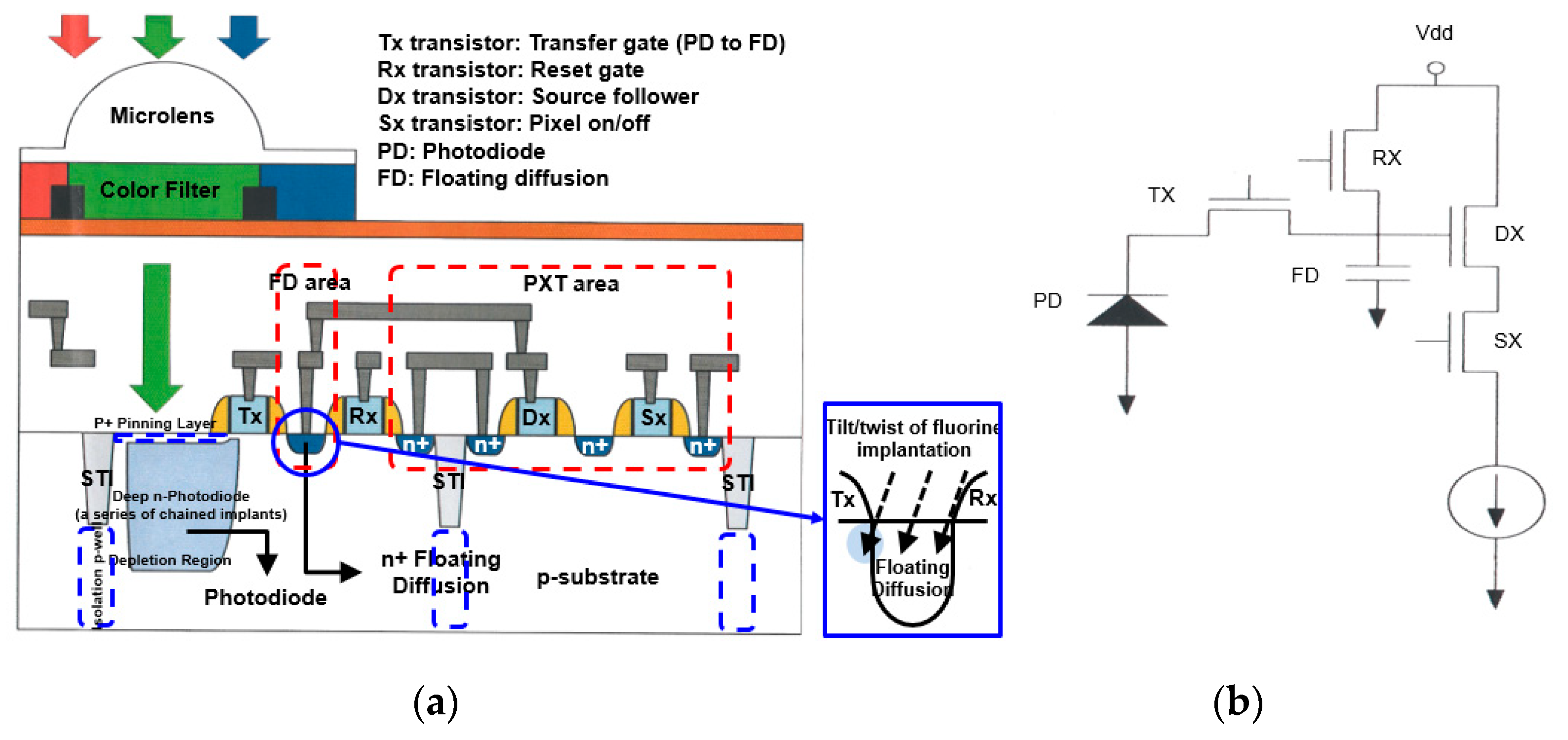
2.2. Principle of Image Sensor Operation

Figure 1 is the schematic drawings of an image sensor. The light receiving part of the image sensor is composed of a micro-lens for efficiently integrating as much light as possible and a color filter for transmitting only a specific color. In addition, there are photodiodes (PD) that generate electrons by receiving transmitted light and a transfer transistor (Tx) that moves signal electrons to floating diffusion (FD) which converts signal electrons to voltage. In addition to the transfer transistor, there are three additional transistors for the analog circuit operation which are a reset transistor (Rx), an amplifier transistor (Dx), and a select transistor (Sx). Here, three transistors are divided into a PXT (pixel transistor) region to distinguish the N+ formation of the transistor.
The operation principle of the image sensor is that when an intended amount of light is incident on the photodiode, the light energy reaches a depletion region inside the photodiode shown in Figure 1, and an electron-hole pair is generated by the light energy. Subsequently, in the electron-major pair, according to the energy distribution, all of the holes in the P-type photodiode are drained to ground, and the electrons are collected into the N-type photodiode. Next, the operation of analog circuits for reading out electrons collected in the photodiode is carried out. When photoelectrons are accumulated in the photodiode for a certain period of time, the reset transistor is turned on and off after the select transistor is turned on, thereby resetting the voltage of the FD of the amplifying transistor. At this time, the signal is read once. Immediately after that, the transfer transistor is turned on and off, and electrons from the photodiode are transferred to the FD. Then, it is immediately read again, and the difference from the previous reset voltage is stored as an image signal of the pixel [4].

3. Experimentals

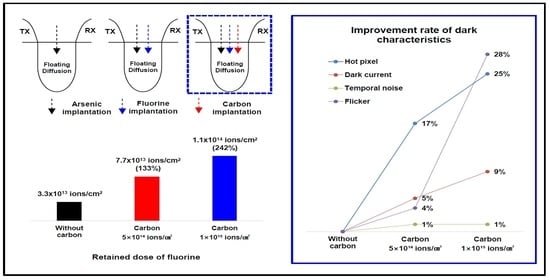
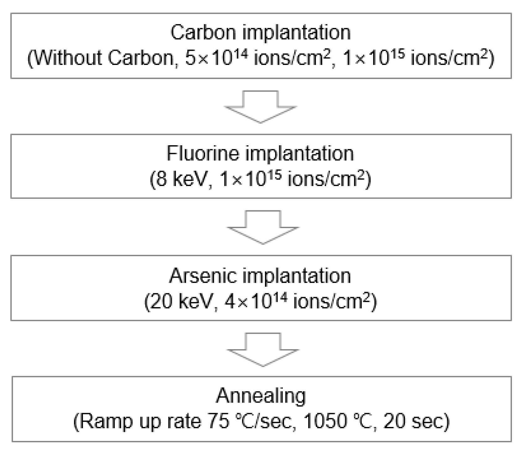
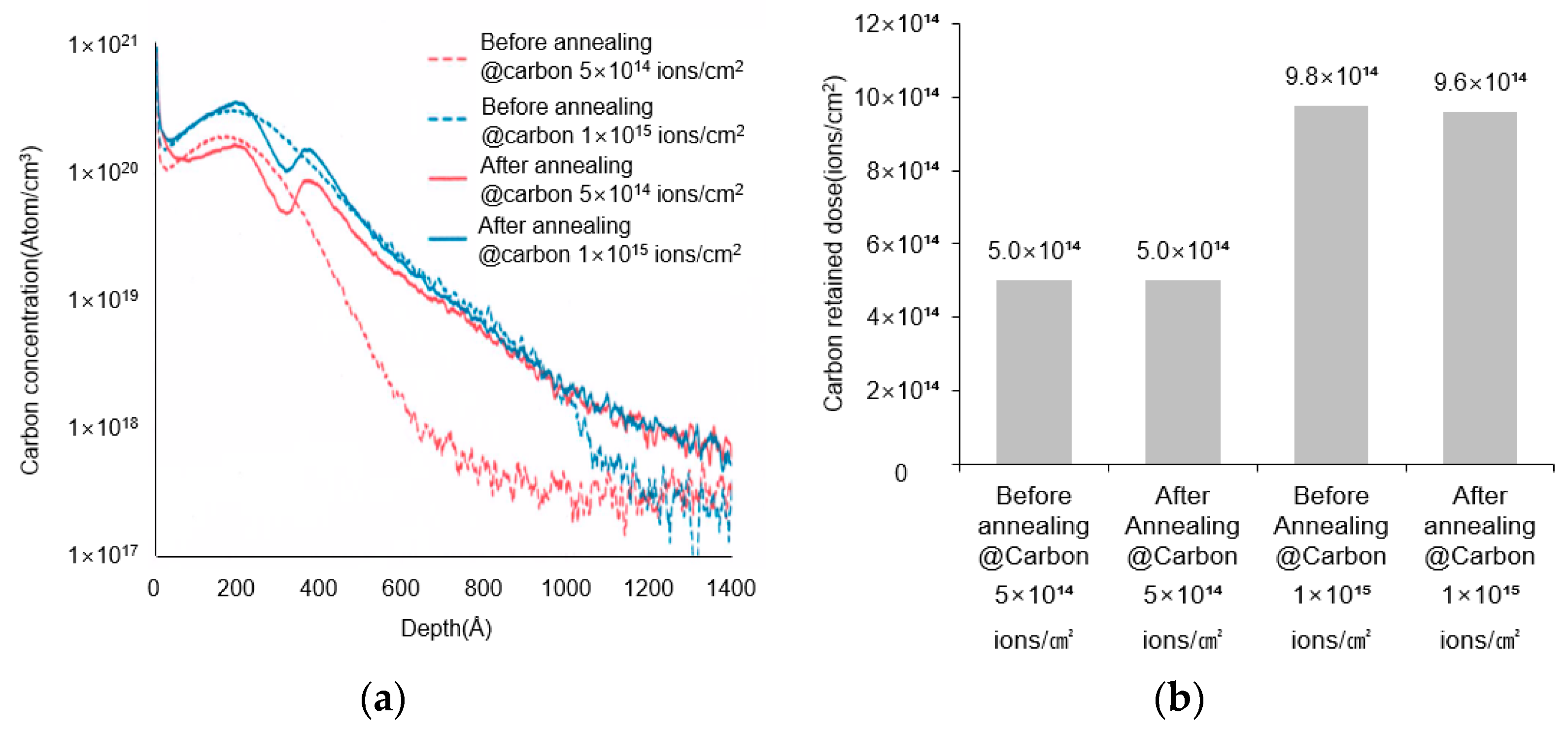
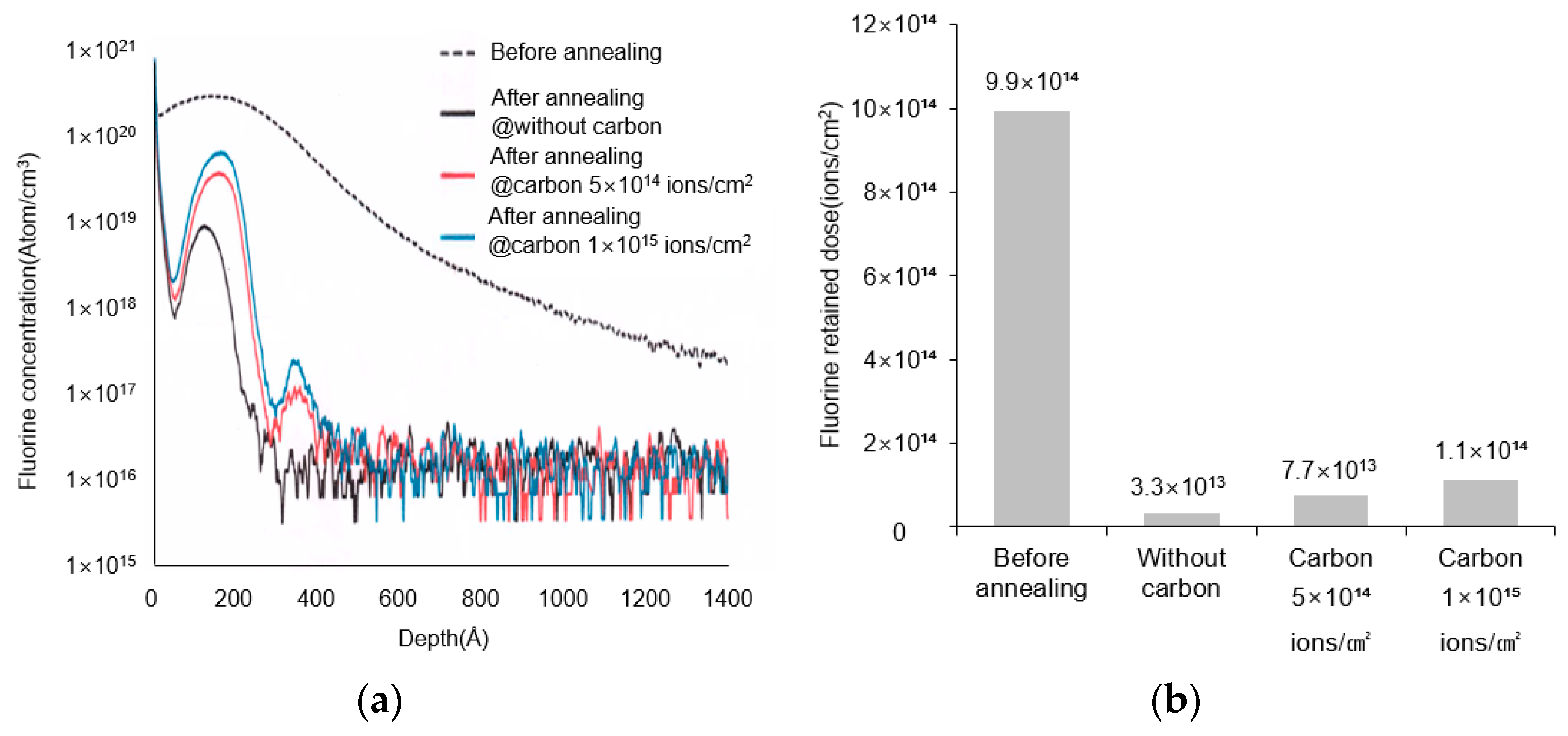
3.1. Implantation Process and Characterization

First, only the N+ formation process was applied on the silicon wafer in order to investigate the effect of the carbon implantation on the diffusion of fluorine and on the dark current characteristics. The total of four P-type silicon wafers (100) with the size of 300 mm were used. Since the N+ formation process conditions can affect each transistor differently, the carbon implantation was applied only to the FD region, which is the drain of the transfer transistor, excluding the PXT region. That is, in order to measure the dark current characteristics, the ions were implanted into the region of the pixel’s transfer transistor floating diffusion. Figure 2 exhibits the flow chart of the overall process. As a first step, the carbon was implanted into the P-type bare silicon wafers with the size of 300 mm without special treatment. The three different dose conditions were applied on the wafer which were no carbon implantation, 5 × 10¹⁴ ions/cm2, and 1 × 10¹⁵ ions/cm2. The implanted energy was 5 keV. After carbon implantation, the fluorine implantation was carried out with an energy of 8 keV and a dose of 1 × 10¹⁵ ions/cm2. As shown in Figure 1a, in order to minimize trap state at the Si-SiO2 interface, the fluorine implantation was performed under the conditions of tilt 15° and twist 90° so that ions can be implanted into the silicon region at the bottom layer of SiO2 in the transfer transistor gate. As the third process, arsenic (As) was implanted with the implantation energy of 20 keV of and a dose of 4 × 10¹⁴ ions/cm2. High current implanter (VIISta Trident, AMAT, CA, USA) was used as the ion implantation equipment. Finally, the annealing process was conducted at 1050 °C for 20 s under conditions of a ramp up rate of 75 °C/s using RTP equipment (Vantage, AMAT, CA, USA). To determine the effect on the ion implantation, the sheet resistance of the wafer was measured using a sheet resistance meter (VR120SD, KOKUSAI, Tokyo, Japan) at a 4-point probe station. Forty-nine points in the wafer were measured, and the average value was used. SIMS (secondary ion mass spectrometry) (SC-Ultra, CAMECA, Gennevilliers, France) was used to analyze the concentrations of arsenic, fluorine and carbon implanted into the wafer after ion implantation.

3.2. Fabrication of Image Sensor

In order to analyze the characteristics of the dark current, the operation of the image sensor is required. Therefore, to measure the dark current, the image sensors were fabricated so that the pixel could operate after the carbon implantation process. For the analysis of dark current characteristics, the implantation of fluorine and carbon was conducted after the gate oxide formation during fabrication of the image sensor. Also, the carbon, fluorine, and arsenic ions were directly implanted to the silicon while the gate oxide was masked with photoresist. That is, the implanted regions for the SIMS analysis and image sensor analysis were both the silicon surface. The dark current characteristics were evaluated under three different carbon implantation conditions: no carbon implantation, dose of 5 × 10¹⁴ ions/cm2, and dose of 1 × 10¹⁵ ions/cm2. After carbon implantation, the image sensors having four transistors (4T) including a pinned photodiode (PPD) were fabricated using a 300 mm P-type silicon wafer (100). The technology of the image sensor was 40 nm, and the number of pixels were 5564 × 4416. As shown in Figure 1, the pinned photodiode pixels are composed of four NMOS transistors including a pinned photodiode (PD), a transfer transistor (Tx), a reset transistor (Rx), an amplifying transistor (Dx), and a select transistor (Sx) [18]. Three image sensor wafers were fabricated for different carbon implantation conditions. Table 1 summarizes the detailed implantation conditions performed in this study. In particular, for ③⑤⑦ process, the image sensor was manufactured to measure the dark current. The image sensor performances, especially the dark current characteristics including dark current, hot pixels, and temporary noise, were measured with the Advantest T2000 equipment.

4. Results and Discussion

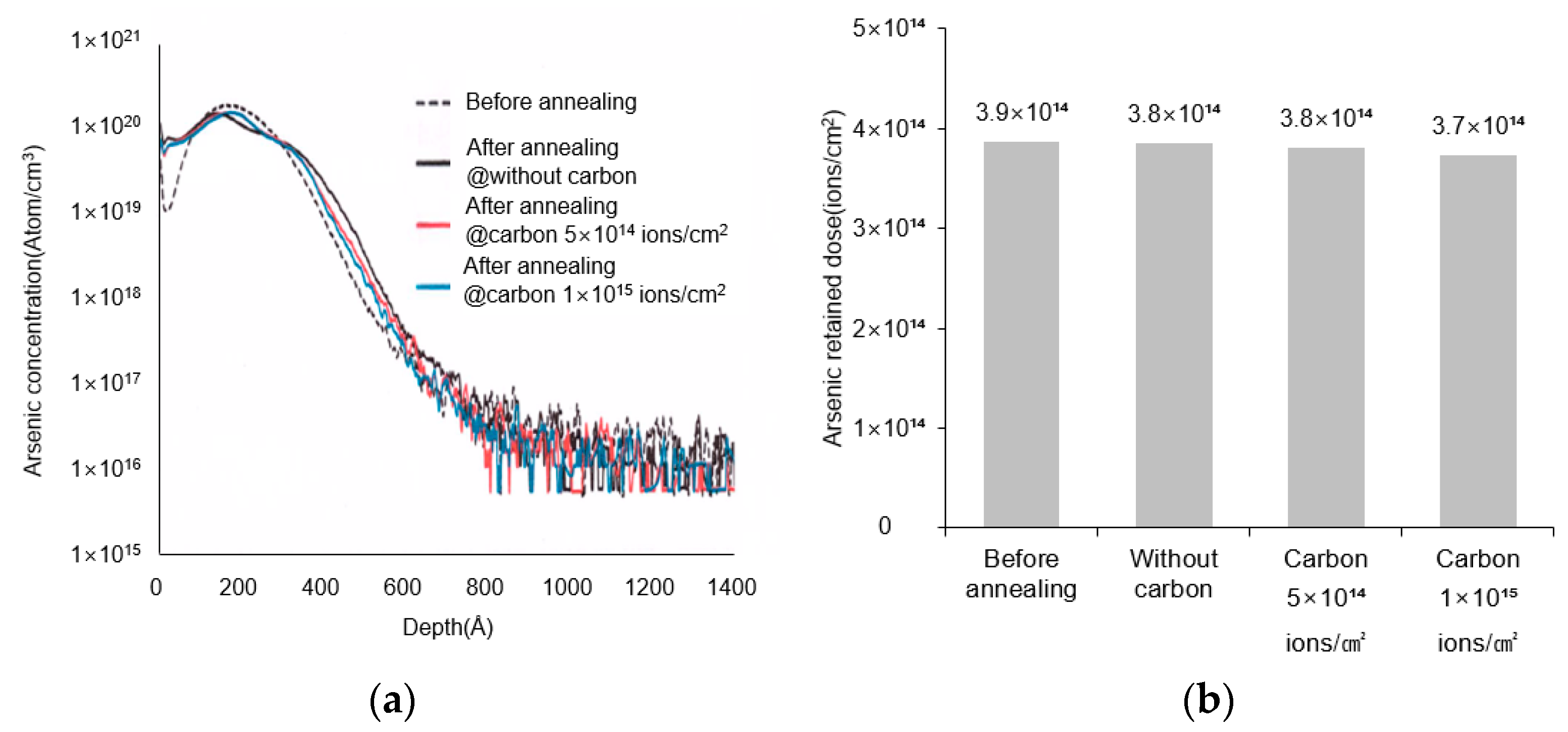
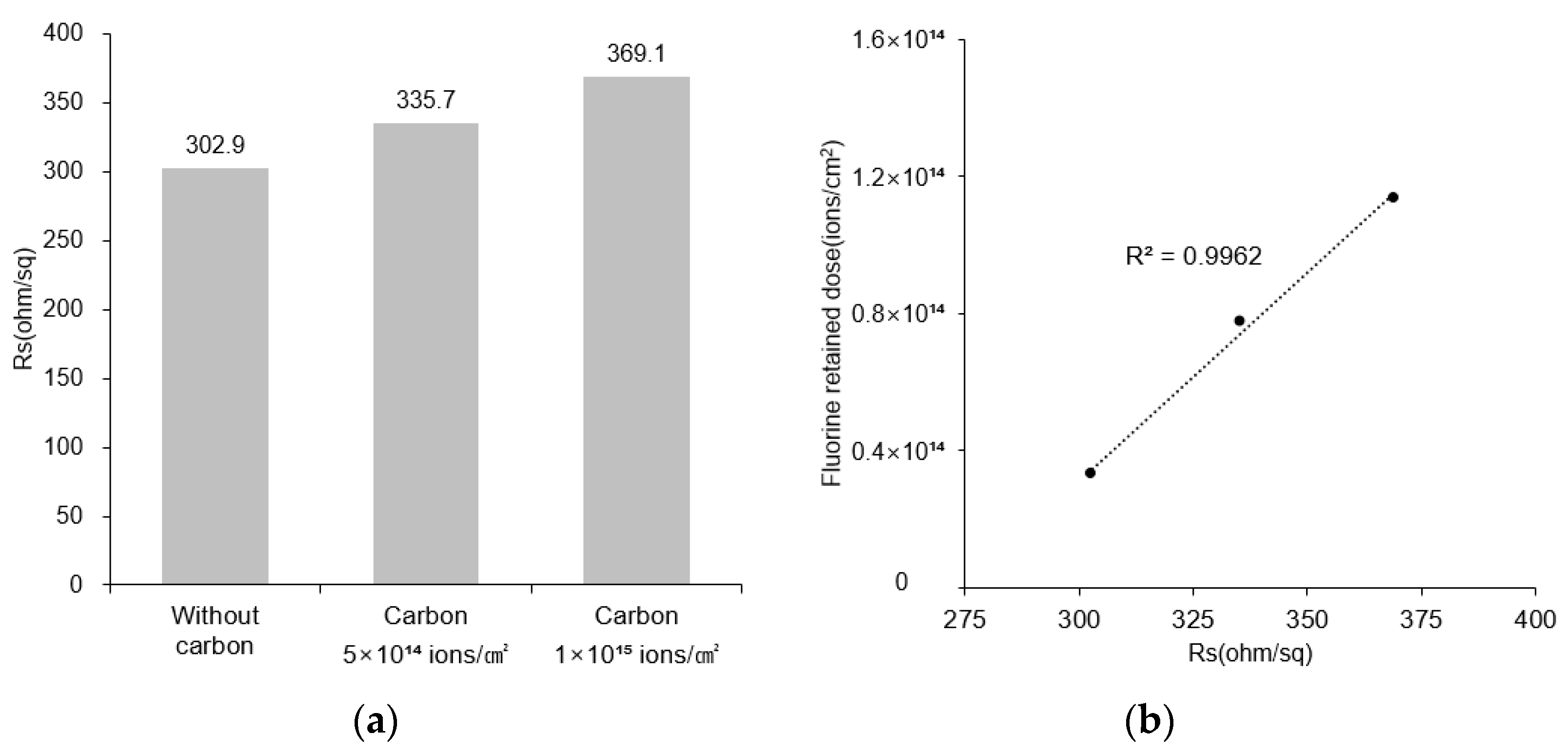
4.1. Measurements of Concentration and Sheet Resistance

The SIMS analysis was performed to analyze the changes in concentration of carbon, fluorine, and arsenic ion according to the depth into the wafer before and after the annealing process. The influence of the carbon concentration on the fluorine diffusion, the defect region of the EOR generated during implantation, and concentration change after the annealing process were analyzed. Figure 3a shows the SIMS profile of the carbon concentration before and after annealing for the case where only carbon is implanted into the wafer. When the carbon was implanted with a dose of 5.0 × 10¹⁴ ions/cm2, it was found that the carbon was evenly diffused throughout the depth direction of the wafer after the annealing process. On the while, in the case of the carbon with a dose of 1.0 × 10¹⁵ ions/cm2, there was little change in concentration before and after the annealing process. It should be noted that when looking at the carbon concentration curve after the annealing, two peaks were formed, of which the concentration of carbon was highest in the first peak occurring at a depth of 200 Å. It was thought that this region is a defect band in the EOR region generated during carbon implantation, which is the boundary between the amorphous region and the single crystal region, and after the annealing process, most of the carbon was accumulated in this region, thus the carbon concentration is considered to be the highest in this region [16].
If we integrate the carbon concentration of the SIMS profile in Figure 3a, we can obtain the retained dose of carbon remaining after the annealing as shown in Figure 3b. In the case of the carbon implantation of 5.0 × 10¹⁴ ions/cm2, it can be seen that the carbon retention dose before and after the annealing was around 5.0 × 10¹⁴ ions/cm2, indicating that there was no change in the carbon retention dose after the annealing process. In the case of high carbon dose of 1.0 × 10¹⁵ ions/cm2, the carbon retention dose before annealing was 9.8 × 10¹⁴ ions/cm2, and the carbon retention dose after annealing was 9.6 × 10¹⁴ ions/cm2, indicating that there was no significant change in the retained dose. That is, it can be seen that the implanted carbon did not diffuse to the outside after the annealing and remained in the wafer.
Figure 4a shows the concentration of fluorine remained in the wafer before and after the annealing, in which fluorine with a dose of 1 × 10¹⁵ ions/cm2 was additionally implanted into the wafer after carbon implantation. Three different carbon implantation condition were also used: no carbon implantation, and the doses of 5.0 × 10¹⁴ ions/cm2, and dose of 1.0 × 10¹⁵ ions/cm2. The concentration of fluorine decreased after annealing implying that fluorine was mostly diffused to the outside of silicon after annealing. In particular, when the carbon was not implanted, the concentration of carbon after the annealing decreased significantly. In case of high carbon dose of 1.0 × 10¹⁵ ions/cm2, the fluorine concentration after annealing is high. In addition, the largest peak of fluorine was found at a depth of 200 Å, which is the same location as the carbon SIMS profile in Figure 3a, and it can be seen that fluorine remains at a high concentration in this region.
In this region, the implanted carbon interacts with some of the point defects in the silicon, and also interacts with the vacancies generated near the surface. This interaction will prevent the diffusion of fluorine at high temperatures after the fluorine implantation. On the other hand, when only the fluorine is implanted without carbon implantation, the vacancies in which the fluorine is present extends well to the EOR and is initially rich near the silicon surface. However, during the annealing at high temperatures, the fluorine becomes rich and eventually diffused to outside. As mentioned above, this region is a defect band in the EOR region that was created during implantation, and the fluorine was not diffused due to carbon, therefore the fluorine concentration became the highest in this region [16]. Figure 4b is the results of the retained dose of fluorine remained after annealing by calculation of integrating the SIMS profile. In the absence of carbon implantation, the fluorine concentration after the annealing was reduced sharply compared to before the annealing. That is, the concentration of fluorine decreased due to diffusion of fluorine to the outside of the silicon surface. In the absence of carbon implantation, the retained dose of fluorine remained after annealing is 3.3 × 10¹³ ions/cm2. On the while, when the carbon was implanted with 5.0 × 10¹⁴ ions/cm2, the retained dose of fluorine was 7.7 × 10¹³ ions/cm2, indicating that 131% of fluorine remained more than when there was no carbon. As the carbon was implanted with 1 × 10¹⁵ ions/cm2, the retained dose of fluorine was 1.1 × 10¹⁴ ions/cm2, indicating that 242% of fluorine remained more. Therefore, it was found that the higher dose of the carbon implantation, the higher the retained dose of fluorine after annealing. Similar to the results reported that the implantation of carbon has the effect of inhibiting the diffusion of boron [16], the carbon implantation acts in the same way for fluorine, thereby preventing the diffusion of fluorine.
The interaction between carbon and fluorine can be summarized as follows. Numerous defects occur in the silicon wafer during the semiconductor manufacturing process. These defects should be minimized since they can affect the electrical activation of the transistor. Among many defects, the representative defects are point defects, and point defects can be classified into defects caused by internal factors and defects caused by external factors. Defects caused by internal factors are also classified into vacancy defects and self-interstitial defects, and defects caused by external factors are classified into substitution foreign atoms and interstitial foreign atoms. Atoms presented in the silicon wafer will diffuse through interactions with these defects.
When the fluorine is implanted into the single crystal silicon and then annealing process is performed, besides the Si self-interstitials defect, the point defect F interacts with the vacancies generated near the surface during implantation. The most stable cluster F that can form in this region is the fluorine-vacancy cluster (FnVm) [19,20,21]. This cluster is immobile, but will be annihilated by interstitials defect at high temperature. That is, the vacancies concentration in the fluorine-implanted region extends well into the EOR, and the FnVm clusters near the silicon surface are initially vacancies-rich, but become fluorine-rich after annealing process [16,22].
In order to control the diffusion of the fluorine, it is assumed that interactions will occur when the fluorine is implanted followed by the carbon implantation. The reason for implanting the carbon first is to increase the diffusion reduction mechanism of the carbon through the interaction of the carbon with some of the existing point defects of the silicon before fluorine interaction. it is generally agreed that any fluorine remaining after a high temperature annealing is trapped by crystalline defects [16,22,23]. That is, more fluorine can be trapped in the case of additionally implanting carbon compared to the case of implanting only fluorine because additional crystal defects [24] are generated. Thus, the con-centration of the fluorine is increased in the crystal defect region and the EOR region created by carbon implantation.
The presence and concentration of arsenic play an important role in transistor operation, such as threshold voltage and contact resistance, thus the arsenic concentration should not be changed as much as possible. It was known that when the arsenic concentration increased, the threshold voltage and contact resistance decreased, and when the arsenic concentration decreased, the threshold voltage and contact resistance increased, thereby causing a change in the operation of the transistor. Figure 5a shows the concentration of arsenic after the carbon implantation before and after annealing process. It can be seen that there is no significant difference in the concentration of arsenic after the annealing compared to before the annealing, and there is little change in the concentration of arsenic according to the carbon implantation conditions. Figure 5b exhibits the retained dose value of the calculated arsenic concentration. The arsenic concentration decreases slightly when annealing is carried out, but there is no significant difference. In addition, there is almost no difference in the concentration of arsenic before and after annealing with respect to the different carbon implantation conditions.
Next, the sheet resistance was measured for the wafer implanted with carbon, fluorine, and arsenic, respectively. As shown in Figure 6a, the sheet resistance for the various implantation conditions of no carbon, carbon dose of 5 × 10¹⁴ ions/cm2, and 1 × 10¹⁵ ions/cm2 were 302.9, 335.7, and 369.1 ohm/sq., respectively. The sheet resistance increased as the implanted carbon dose increased. In conclusion, as the carbon implantation dose increased, the fluorine concentration increased, and the increase of the fluorine concentration had a great influence on the increase of the sheet resistance. Also, as shown in Figure 6b, the correlation between sheet resistance and the retained dose of fluorine shows that R2 (correlation coefficient) is 0.99, indicating the very strong relationship. Therefore, an increase in carbon concentration contributed to an increase in the retained dose of fluorine. The passivation region of unsaturated bonds increased due to the increase in fluorine, and the minority carriers of electrons or holes decreased by strong Si-F bonds as the passivation region increased. As a result, the sheet resistance increased. That is, carrier mobility was reduced.

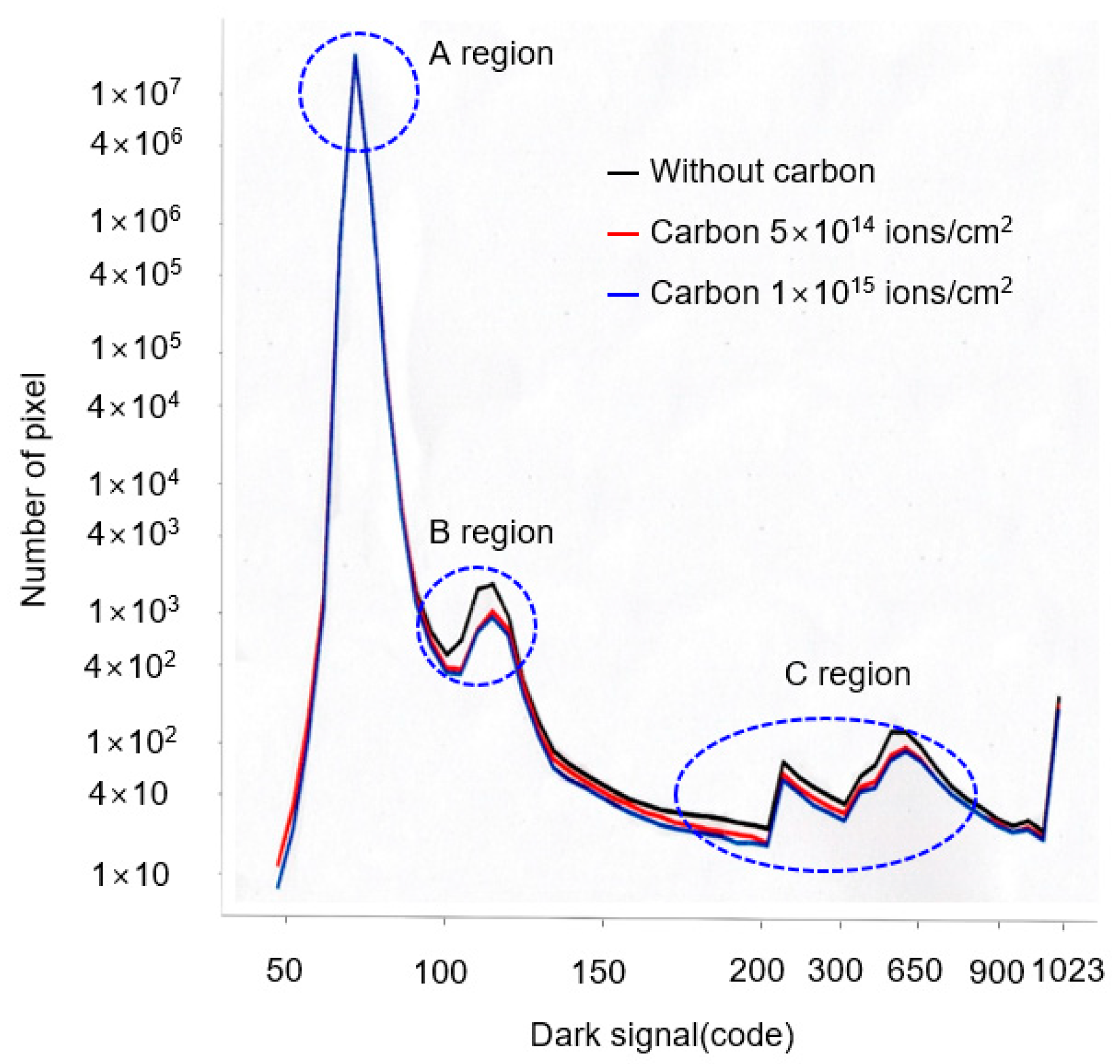
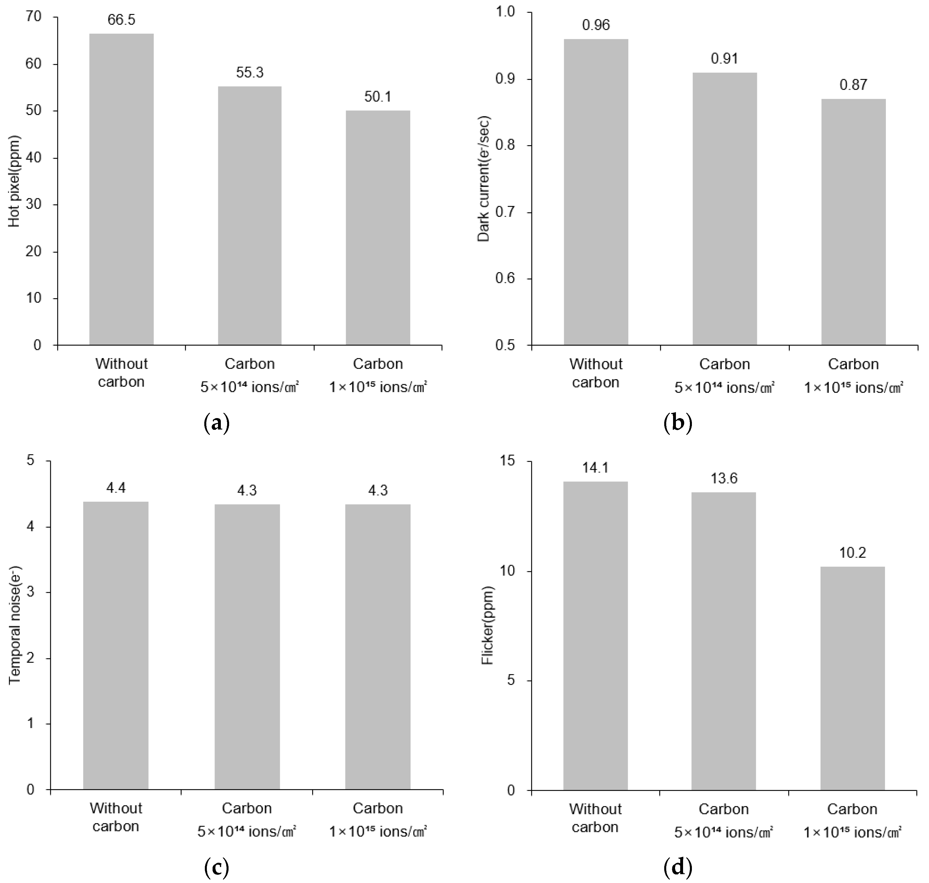
4.2. Evaluation of Dark Current of Image Sensor

The dark current characteristics of the image sensor were measured by fabricating the image sensors, and evaluations of defective pixels, dark current, temporary noise, and flicker were performed, respectively. The dark current was generally evaluated with measuring the current flow by changing the voltage on the image sensor in the absence of light. In this study, the dark current characteristics were analyzed by digitizing the behavior of the dark current of the image sensor and converting the code. The dark current of each pixel was converted into a voltage, and a dark current histogram was created in which the voltage was expressed in a 10-bit code format [25,26,27,28]. Firstly, we took 15 images under the condition of 60 °C without light, and calculated the average value of the output code generated from each image. After that, we converted the output voltage for each pixel into a code based on 10 bits. Finally, we could obtain a dark current histogram for three different carbon implantation conditions as shown in Figure 7: a carbon-free, a carbon does of 5 × 10¹⁴ ions/cm2, and a carbon dose of 1 × 10¹⁵ ions/cm2. In the figure, the vertical axis means the number of pixels. In the case of carbon implantation, it can be seen that the number of larger than 100 codes in the dark histogram is mostly reduced compared to the condition without carbon implantation. In particular, the second peak in the 100–150 code region has significantly decreased. As shown in Figure 7, the overall improvement of the dark current was observed after the carbon implantation. To explain the cause of the improvement, the peak regions in Figure 7 were divided into the regions A, B, and C. The region A is the dark signal generated in all pixel signals. The region B and C are the regions of the bright pixels that have an additional defect generating additional charge. The main cause of the dark current improvement in the region B was the reduction of the trap state. On the while, the main cause of the improvement in the region C was the reduction of the leakage current due to the reduction of the minority carriers.
From the dark current histogram of Figure 7, the defective pixels (hot pixel) in ppm units can be calculated by dividing the number of pixels with more than 200 codes by the total number of pixels in 10−6 units as shown in Figure 8a. That is, it is a pixel having a charge that exhibits a brightness of 20% or more in the absence of light which is expressed in ppm units. In the case of no carbon implantation, the defective pixel is 66.5 ppm. In the case of the carbon dose of 5.0 × 10¹⁴ and 1 × 10¹⁵ ions/cm2, the defective pixels are 55.3 and 50.1 ppm, respectively. Therefore, the defective pixel was improved by 17% and 25% for the case of the carbon dose of 5.0 × 10¹⁴ and 1 × 10¹⁵ ions/cm2 compared to the case in which there is no carbon implantation. Figure 8b is the dark current value. The dark current was measured by the amount of electrons generated in the PD under a temperature of 60 °C in the absence of light, and calculated by converting the output value according to the exposure time into a slope. The dark current without carbon implantation was 0.96 e/s, on the while, the dark current under the carbon dose of 5.0 × 10¹⁴ and 1 × 10¹⁵ ions/cm2 was 0.91 and 0.87 e/s, respectively, indicating that the dark current with carbon implantation decreased by about 9.4% compared to the condition without carbon implantation.
Noise refers to the amplification or reduction of an unwanted signal. And, the temporary noise means noise that changes over time. The temperature noise can be calculated by following process; after 100 images were taken under room temperature conditions in the absence of light, the standard deviation value for the code fluctuations between pixels in the entire image area was calculated as an average value and converted to e unit to measure the temporary noise. The measured values for temporary noise are shown in Figure 8c. Temporary noise under the condition without carbon implantation was measured to be 4.4 e, and the temporary noise under carbon dose of 1 × 10¹⁵ ions/cm2 was 4.3 e, which was not a big difference compared to the condition without carbon, but the temporary noise was slightly improved. Figure 8d exhibits the measurement result for flicker. Flicker means random noise. After creating several images under room temperature conditions in the absence of light, the number of pixels whose output values of 20 images have a difference of ±30 codes or more is divided by the total number of pixels in units of 10−6, then the flicker can be calculated in ppm units as shown in Figure 8d. It can be seen that the flicker in the condition without carbon was 14.1 ppm, and the flicker generated in the carbon dose of 5.0 × 10¹⁴ and 1 × 10¹⁵ ions/cm2 was 13.6 and 10.2 ppm, respectively, showing about 28% improvement of flicker compared to the condition without carbon implantation.
In conclusion, when carbon was implanted, the overall characteristics of the dark current of the image sensor such as defective pixels, dark current, temporary noise, and flicker were improved. These results indicated the effectiveness of the carbon implantation by reducing the external diffusion of fluorine, and the remained fluorine was effective in improving the dark current characteristics of the image sensor.

5. Conclusions

In this paper, we analyzed the effects of carbon implantation on the diffusion of fluorine to the outside of the silicon surface after annealing before fluorine implantation in the N+ formation process of FD region in the CMOS image sensor. In particular, we investigated the effectiveness of the carbon implantation on enhancing the dark current characteristics of the CMOS image sensor. It was confirmed that the higher concentration of the carbon implantation, the higher the retained dose of fluorine after annealing. As the carbon was implanted with a dose of 5.0 × 10¹⁴ ions/cm2, the retained dose of fluorine was 7.7 × 10¹³ ions/cm2, indicating that 131% more fluorine remained than no carbon implantation. As the carbon was implanted with 1 × 10¹⁵ ions/cm2, the retained dose of fluorine was 1.1 × 10¹⁴ ions/cm2, indicating that 242% more fluorine remained. As the retained fluorine concentration increased, the minority carriers of electrons or holes decreased by more Si-F bond formation, resulting in increasing the sheet resistance. Therefore, the retained fluorine dose and the sheet resistance had a very close relationship. When carbon was implanted with 5.0 × 10¹⁴ ions/cm2, the defective pixel, dark current, transient noise, and flicker were improved by 17%, 5%, 1%, and 4%, respectively, compared to the condition without carbon implantation. In case of the carbon implantation of 1.0 × 10¹⁵ ions/cm2, the defective pixel, dark current, transient noise, and flicker were much improved by 25%, 9.4%, 1%, and 28%, respectively. In conclusion, it was found that the diffusion of fluorine after annealing could be controlled by the carbon implantation, and the dark current characteristics were improved as the remaining fluorine concentration increased.

Author Contributions

The manuscript was written using contributions of S.-Y.C. and S.-H.C. All authors have read and agreed to the published version of the manuscript.

Funding

This research received no external funding.

Institutional Review Board Statement

Not applicable.

Informed Consent Statement

Not applicable.

Data Availability Statement

Not applicable.

Acknowledgments

This research was conducted with the support of the Seoul National University of Science and Technology academic research grant.

Conflicts of Interest

The authors declare no conflict of interest.

References

  1. Market Breakdown of Camera Phone—2nd Half 2019 & 1st Half 2020 Forecast; Techno Systems Research: Tokyo, Japan, 2020; pp. 1–4. Available online: https://www.t-s-r.co.jp/en/report/3115/ (accessed on 10 September 2021). (In Japanese)
  2. Sukhavasi, S.B.; Sukhavasi, S.B.; Elleithy, K.; Abuzneid, S.; Elleithy, A. CMOS Image Sensors in Surveillance System Applications. Sensors 2021, 21, 488. [Google Scholar] [CrossRef] [PubMed]
  3. Park, S.-S.; Shin, B.-J.; Uh, H.-S. Recent Technology Trends and Future Prospects for Image Sensor. J. Microelectron. Packag. Soc. 2020, 27, 1–10. [Google Scholar]
  4. Park, S.-S. CCD/CMOS Image Sensor; Dooyangsa: Seoul, Korea, 2010; pp. 43–140. [Google Scholar]
  5. Teranishi, N.; Kohono, A.; Ishihara, Y.; Oda, E.; Arai, K. No Image Lag Photodiode Structure in the Interline CCD Image Sensor. In Proceedings of the International Electron Devices Meeting, San Francisco, CA, USA, 13–15 December 1982; pp. 324–327. [Google Scholar]
  6. Fossum, E.R.; Hondongwa, D.B. A Review of the Pinned Photodiode for CCD and CMOS Image Sensors. IEEE J. Electron Devices Soc. 2014, 2, 33–43. [Google Scholar] [CrossRef]
  7. Teranishi, N. Effect and Limitation of Pinned Photodiode. IEEE Trans. Electron Devices 2015, 63, 10–15. [Google Scholar] [CrossRef]
  8. Teranishi, N. Ion Implantation Technology for Image Sensors. In Proceedings of the 21st International Conference on Ion Implantation Technology (IIT), Tainan, Taiwan, 26–30 September 2016; pp. 1–6. [Google Scholar]
  9. Teranishi, N.; Fuse, G.; Sugitani, M. A Review of Ion Implantation Technology for Image Sensors. Sensors 2018, 18, 2358. [Google Scholar] [CrossRef] [PubMed] [Green Version]
  10. Chern, H.-N.; Lee, C.-L.; Lei, T.-F. The Effect of Fluorine Passivation on Polysilicon Thin-Film Transistors. IEEE Trans. Electron Devices 1994, 41, 698–702. [Google Scholar] [CrossRef]
  11. Kwon, S.-K.; Kwon, H.-M.; Han, I.-S.; Jang, J.-H.; Oh, S.-H.; Song, H.-S.; Park, B.-S.; Chung, Y.-S.; Lee, J.-H.; Kim, S.-B.; et al. Effects of Fluorine on the NBTI Reliability and Low-Frequency Noise Characteristics of p-MOSFETs. IEEE J. Electron Devices Soc. 2018, 6, 808–814. [Google Scholar] [CrossRef]
  12. Maegawa, S.; Ipposhi, T.; Maeda, S.; Nishimura, H.; Ichiki, T.; Ashida, M.; Tanina, O.; Inoue, Y.; Nishimura, T.; Tsubouchi, N. Performance and Reliability Improvements in Poly-Si TFT’s by Fluorine Implantation into Gate Poly-Si. IEEE Trans. Electron Devices 1995, 42, 1106–1112. [Google Scholar] [CrossRef]
  13. Ha, M.-L.; Kang, M.-K.; Yoon, S.-W.; Han, C.-H.; Lee, J.; Lee, Y.-J. Temporal Noise Improvement Using the Selective Application of the Fluorine Implantation in the CMOS Image Sensor. In Proceedings of the International Image Sensors Workshop (IISW), Hiroshima, Japan, 30 May–2 June 2017; pp. 32–35. [Google Scholar]
  14. Mastromatteo, M. Mechanism of Fluorine redistribution and Incorporation During Sold Phase Epitaxial Regrowth of Pre-Amorphized Silicon. Ph.D. Thesis, University of Padova, Padua, Italy, 31 January 2010. [Google Scholar]
  15. Jeng, S.-P.; Ma, T.-P.; Canteri, R.; Anderle, M.; Rubloff, G.W. Anomalous Diffusion of Fluorine in Silicon. Appl. Phys. Lett. 1992, 61, 1310–1312. [Google Scholar] [CrossRef] [Green Version]
  16. Vanderpool, A.; Taylor, M. Reducing Ultra-Shallow Boron Diffusion Using Carbon and Fluorine Co-implantation. Nucl. Instrum. Methods Phys. Res. Sect. B Beam Interact. Mater. Atoms. 2005, 237, 142–147. [Google Scholar] [CrossRef]
  17. Williams, J.S. Solid phase epitaxial regrowth phenomena in silicon. Nucl. Instr. Meth. Res. 1983, 209–210, 219–228. [Google Scholar] [CrossRef]
  18. Nakamura, J. Image Sensors and Signal Processing for Digital Still Cameras; Taylor & Francis Group Publisher: London, UK, 2006; pp. 156–157. [Google Scholar]
  19. Diebel, M.; Chakravarthi, S.; Dunham, S.T.; Machala, C.F.; Ekbote, S.; Jain, A. Investigation and Modeling of Fluorine Co-implantation Effects on Dopant Redistribution. MRS Online Proc. Libr. (OPL) 2003, 765, D6.15.1–D6.15.6. [Google Scholar] [CrossRef] [Green Version]
  20. Diebel, M.; Dunham, S.T. Ab-initio Calculations to Model Anomalous Fluorine Behavior. MRS Online Proc. Libr. (OPL) 2002, 717, C4.5.1–C4.5.6. [Google Scholar] [CrossRef]
  21. Dunham, S.T. The Process Modeling Hierarchy: Connecting Atomistic Calculations to Nanoscale Behavior. In Proceedings of the International Conference on Simulation of Semiconductor Processes and Devices (SISPAD), Kobe, Japan, 4–6 September 2002; pp. 213–216. [Google Scholar]
  22. Pi, X.D.; Burrows, C.P.; Coleman, P.G. Fluorine in Silicon: Diffusion, Trapping, and Precipitation. Phys. Rev. Lett. 2003, 90, 155901. [Google Scholar] [CrossRef]
  23. Mubarek, H.A.W.E.; Ashburn, P. Reduction of Boron Diffusion in Silicon-Germanium by Fluorine Implantation. IEEE Electron Device Lett. 2004, 25, 535–537. [Google Scholar] [CrossRef]
  24. Titov, A.I.; Karabeshkin, K.V.; Karaseov, P.A.; Struchkov, A.I. Do chemical effects affect the accumulation of structural damage during the implantation of fluorine ions into GaN? Semiconductors 2019, 53, 1415–1418. [Google Scholar] [CrossRef]
  25. Carrère, J.P.; Place, S.; Oddou, J.P.; Benoit, D.; Roy, F. CMOS Image Sensor: Process Impact on Dark Current. In Proceedings of the 2014 IEEE International on Reliability Physics Symposium, Waikoloa, HI, USA, 1–5 June 2014; pp. 3C.1.1–3C.1.6. [Google Scholar]
  26. Domengie, F.; Regolini, J.L.; Bauza, D.; Morin, P. Impact on Device Performance and Monitoring of Low Dose of Tungsten Contamination by Dark Current Spectroscopy. In Proceedings of the 2010 IEEE International Reliability Physics Symposium (IRPS 2010), Anaheim, CA, USA, 2–6 May 2010; pp. 259–264. [Google Scholar]
  27. Virmontois, C.; Goiffon, V.; Magnan, P.; Girard, S.; Saint-Pé, O.; Petit, S.; Rolland, G.; Bardoux, A. Influence of Displacement Damage Dose on Dark Current Distributions of Irradiated CMOS Image Sensors. In Proceedings of the 2011 12th European Conference on Radiation and Its Effects on Components and Systems, Seville, Spain, 19–23 September 2011; pp. 329–335. [Google Scholar]
  28. Janesick, J. Photon Transfer DN→λ; SPIE Press: Bellingham, WA, USA, 2007; pp. 35–38. [Google Scholar]
Figure 1. (a) Cross-sectional illustration of CMOS image sensor. (b) Schematics of 4T pixel structure.
Crystals 11 01106 g001
Figure 2. Flow chart of the overall process including implantation and annealing process.
Crystals 11 01106 g002
Figure 3. (a) SIMS profile of carbon concentration before and after annealing. (b) Retained dose of carbon in the wafer.
Crystals 11 01106 g003
Figure 4. (a) SIMS profile of fluorine concentration remained in the wafer before and after the annealing. (b) Retained dose of fluorine in the wafer.
Crystals 11 01106 g004
Figure 5. (a) SIMS profile of arsenic concentration after carbon implantation before and after annealing process. (b) Retained dose of fluorine in the wafer.
Crystals 11 01106 g005
Figure 6. (a) Measurement results of sheet resistance. (b) Correlation between sheet resistance and the retained dose of fluorine.
Crystals 11 01106 g006
Figure 7. Dark current histogram in conditions of carbon-free, carbon dose of 5 × 10¹⁴ ions/cm2, and carbon dose of 1 × 10¹⁵ ions/cm2.
Crystals 11 01106 g007
Figure 8. Measurement results of dark current characteristics. (a) hot pixel, (b) dark current, (c) temporal noise, (d) flicker.
Crystals 11 01106 g008
Table 1. Detailed implantation conditions and order with measurements of dark current characteristics.
Process OrderProcess Item & ConditionWithout CarbonCarbon
5 × 10¹⁴ Ions/cm2
Carbon
1 × 10¹⁵ Ions/cm2
1Carbon
implantation
5 keV, 5 × 10¹⁴ ions/cm2,
Tilt 0°, Twist 0°
5 keV, 1 × 10¹⁵ ions/cm2,
Tilt 0°, Twist 0°
2Fluorine
implantation
8 keV, 1 × 10¹⁵ ions/cm2,
Tilt 15°, Twist 90°
3Arsenic
implantation
20 keV, 4 × 10¹⁴ ions/cm2,
Tilt 0°, Twist 0°
4AnnealingRamp up rate 75 °C/s,
1050 °C, 20 s
5Rs4-point probe, 49 point
6SIMSCarbon, fluorine, arsenic
7Dark
characteristics
Hot pixel, dark current,
temporal noise, flicker
Publisher’s Note: MDPI stays neutral with regard to jurisdictional claims in published maps and institutional affiliations.

