Article

3D-Printed Metasurface Units for Potential Energy Harvesting Applications at the 2.4 GHz Frequency Band

1
Institute of Electronic Structure and Laser (IESL), Foundation for Research & Technology–Hellas (FORTH), N. Plastira 100, Vassilika Vouton, GR-700 13 Heraklion, Greece
2
Physics Department, University of Crete, Vassilika Vouton, GR-700 13 Heraklion, Greece
*
Authors to whom correspondence should be addressed.
Crystals 2021, 11(9), 1089; https://doi.org/10.3390/cryst11091089
Submission received: 10 August 2021 / Revised: 1 September 2021 / Accepted: 3 September 2021 / Published: 7 September 2021
(This article belongs to the Special Issue 3D Printing/Additive Manufacturing of Alloys, Ceramics and Polymers)

Abstract

:
The capability of three-dimensional printed cut-wire metasurfaces to harvest energy in frequencies around 2.4 GHz, is studied in this paper. Cut-wire metasurfaces were constructed using the Fused Filament Fabrication technique. In particular, two metasurfaces, consisting of different materials were produced. The first was constructed using Polylactic Acid as starting material. Then, the printed metasurface was covered with a thin layer of conductive silver paint, in order to achieve good electrical conductivity. The other metasurface was built using commercially available, conductive Electrifi. Both metasurfaces exhibit good energy harvesting behavior, in the frequency band near 2.4 GHz. Their harvesting efficiency is found to be almost three times lower than that obtained for conventional PCB-printed cut-wire metasurfaces. Nevertheless, all of the experimental results presented here strongly corroborate that three-dimensional-printed metasurfaces can be potentially used to harvest energy in the 2.4 GHz frequency band.

1. Introduction

The metamaterial family includes all those artificially constructed materials, which exhibit tailored interaction with incident electromagnetic radiation, enabling extraordinary functions and properties [1,2]. Up to now, metamaterials and metasurfaces (two- dimensional version of metamaterials, consisting of a single plane meta-atoms) have been realized for a great variety of applications, such as electromagnetic shields, polarizers, sensors, electromagnetic beam splitters, broadband pulse delay devices, etc. [3,4,5,6,7]. Among them, metamaterials for energy harvesting applications gain great interest lately [8,9,10], since metamaterials can be designed in appropriate dimensions, to enable full electromagnetic absorption in certain frequency regimes. In this context, most efforts are focusing on the microwave frequency range in the last decade. Reasons for such an attention include the tremendous evolution of wireless communications (i.e., cell phones and wi-fi gadgets), resulting in an incredible increment of microwave emitting and receiving, including telecommunication antennas, wi-fi hubs, etc. In addition, the wavelength in the microwave regime lays in the range of a few millimeters, which allows the fabrication of metamaterial devices in the millimeter scale, without the cost and difficulties of micro- and nano-fabrication.
To this point, several microwave metamaterial set-ups have been proposed, properly harvesting energy in the range 900 MHz–6 GHz [11,12,13,14,15,16,17,18]. Among them, Erkmen et al. [19] lately, proposed a concentric structure of bow-tie-like periodic absorbers and a full-wave rectifier. Through combined theoretical simulations and experimental verifications, it was shown that the proposed structure effectively performs in microwave regime (efficiency ~60%,) regardless of the incident wave angle, thus a scalable and polarization insensitive energy-harvesting system is achieved. On the other hand, a cross-dipole structure was recently proposed by Ashoor et al. [20]. Such structure behaves qualitatively similar to the previous one, reaching an efficiency of 74%, over all polarization angles. Furthermore, split ring resonators (SRRs) have also been proposed for energy harvesting in the microwave regime [21]. Depending on their dimensions, SRRs perfectly absorb at certain frequencies, thus their over-all radiation-to-DC-power conversion efficiency is enhanced. On the other hand, the design of the antenna in microwave energy harvesting devices is revealed as a key parameter [22]. In this context, metamaterial-based set-ups show a distinctive advantage, since they can be constructed with negligible reflection, and thus the power transfer between the antenna and the rectifier is maximized. Moreover, they seem flexible in terms that the dedicated metamaterial structures and designs can absorb energy from ambient microwave power sources, maximizing the efficiency of the harvesting device.
All of the above mentioned metamaterial units [11,12,13,14,15,16,17,18,19,20,21,22] have been constructed employing the conventional printed circuit (PCB) technology, which permits the high printing resolution and the consequent high quality of the produced metamaterial unit. The electronic industry massively constructs electronic boards and components based on PCB technology, resulting in the high automation of the process and the subsequent cost minimization. However, PCB-printed metamaterials exhibit some severe drawbacks. For example, all metamaterials must be printed on dedicated substrates, such as FR-4. The production of such substrates is a complicated, multi-step process, including, specialized mechanical and chemical procedures. In addition, all PCB-printed metamaterials are strictly planar (two-dimensional), while the presence of the substrate eliminates their flexibility, preventing them from being attached to arbitrarily-shaped surfaces.
During the last years, construction of complex objects is being achieved employing three-dimensional (3D) printing technologies. In principle, 3D printing is an additive manufacturing process, in which a 3D structure is developed by stacking material layers one on top of the other. Several printing methods have been established, so far [23,24]. Among them, the so-called fused filament fabrication (FFF) or fused filament deposition (FDM) is probably the most-widely used. In this method, long plastic wires (filaments) are used as starting materials. These filaments are heated above their melting point and subsequently they are pushed through a nozzle. The nozzle is being moved in the xy plane, drawing a single plastic layer of the desired object. Then, it moves upwards, along the z direction, and draws another layer of the object. By stacking layers one above the other, the final object is printed. The FFF method exhibits all the 3D printing technology advantages (i.e., it is a quick, cost-effective, and user-friendly method), while it possesses individual positive features such as FFF printers with multiple filament printing options, so that different filaments can be printed to construct an object. Moreover, the commercially FFF printers are available in reasonable prices.
To date, the FFF method has been successfully used in constructing metamaterials and metasurfaces for applications in the microwave regime [25,26,27]. Therefore, the fabrication of metasurfaces for microwave energy harvesting seems to be feasible. In this context, we hereby present the fabrication of stand-alone cut-wire metasurface units, and the corresponding, detailed investigation, regarding their energy harvesting capability in the frequency band, around 2.4 GHz. The cut-wire metasurface design has been theoretically studied [18], regarding its harvesting efficiency, to be optimized in the sub-6 GHz regime. For the purposes of the current study, three different metasurface units were developed. The first is a FR-4 built metasurface, which is conventionally printed using PCB technology, and is used as a reference. Another metasurface is constructed, using the FFF method. The polylactic acid (PLA) filament is used as a printing material. The produced metasurface is then covered by a thin layer of conducting silver paint, so that the metasurface becomes conducting. Finally, a third metasurface is developed, employing the FFF method, with the Electrifi filament as the printing material. This filament is considered as the most conductive, commercially available filament, so far.
All three metasurfaces were characterized regarding their electromagnetic (EM) response, by measuring the S 21 parameter as a function of frequency, in order to confirm their good absorbing behavior, in the frequency band, around 2.4 GHz. By including a Schottky diode into the gap of the metasurface, the absorbed energy is transformed to a DC signal, as evidently shown by the corresponding electric measurements. Several experiments were performed to justify that the measured DC signals are not attributed to parasitic effects and artifacts. Moreover, other experiments were performed in order to clarify the optimal configuration, producing maximum DC signals, as well as a maximum output power. Both 3D-printed metasurfaces (PLA- and Electrifi-based ones), harvest in the same manner as the FR-4 one, however, with inferior efficiency. Nevertheless, the use of 3D-printed metasurface units for potential energy harvesting applications in the 2.4 GHz frequency band is clearly demonstrated, in this study.
Regarding the structure of the present paper, the section “Materials and Methods” includes a subsection regarding the cut-wire metasurface construction and another subsection describing the electromagnetic characterization of the metasurfaces. A third subsection demonstrates the experimental configuration used for the energy harvesting verification of the metasurfaces, while the last subsection describes the theoretical simulation tools used, in the current study. The section “Results and Discussion” contains three parts: In the first part, the energy harvesting capability of the FR-4 built metasurface as well as its performance is explored. In the second and third parts, the energy harvesting properties of the Ag/PLA and Electrifi 3D printed metasurfaces, are presented, respectively. Finally, in the “Summary” and “Conclusions” sections, both advantages and disadvantages of the 3D printed metasurfaces are summarized and consequent conclusions are present.

2. Materials and Methods

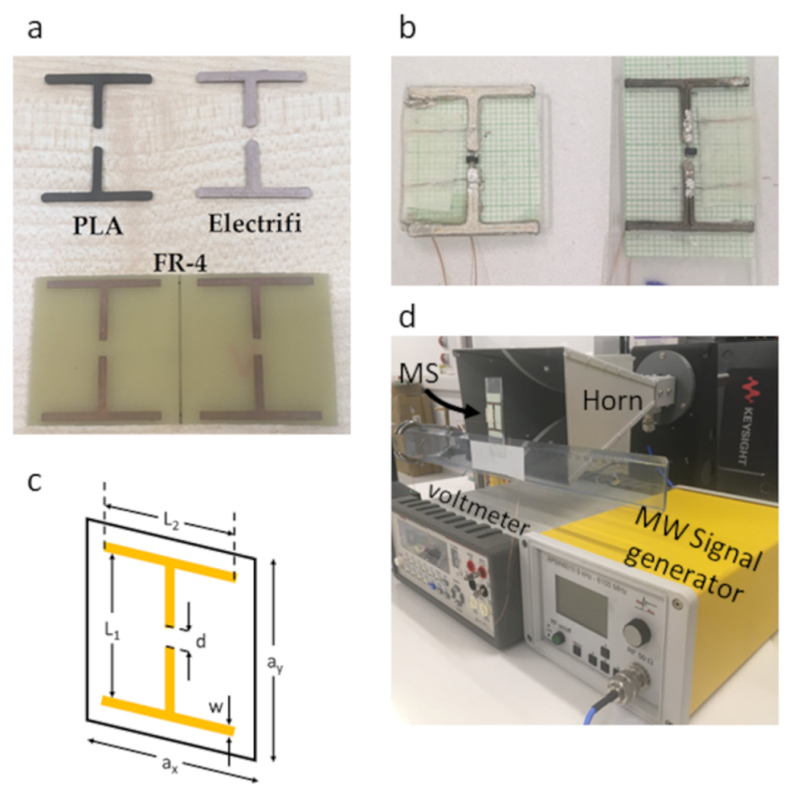
2.1. Metasurface Fabrication

For the purpose of the current study, the cut-wire metasurface (MS) unit, pictured in Figure 1c, is used. The dimensions of the meta-atom (as shown in Figure 1c), are listed in Table 1. Three identical MSs were fabricated. The first one (lower MS unit in Figure 1a) is conventionally developed, i.e., metallic Cu stripes were etched on a single-metallization-layer FR-4 substrate, employing the widely-known PCB technology. This unit will be used as a reference, to compare the other two samples.
The other two MSs were developed employing the FFF method. For this purpose, a commercial FFF 3D printer was used (MakerBot Replicator 2x, New York, NY, USA). The two 3D-printed MSs were different, i.e., the first was printed using a common polylactic acid (PLA) filament, while the other was printed using an Electrifi filament, which is a commercially available conductive filament (Muti3D Inc., CA, USA). Details regarding printing materials, processes, and printing conditions can be found elsewhere [27]. Several, stand-alone, T-like components were printed, from both filaments (i.e., upper units in Figure 1a). Then, pairs of those T-like components were glued onto a piece of millimeter paper, so that the final cut-wire MS unit (Figure 1b) is formed. No EM response of the thin paper sheet was detected in the microwave regime. Therefore, the built MSs are modeled as freestanding metamaterial units.
The materials used in the development of the MSs are quite different, regarding their electrical conductivity. For instance, Cu stripes used in FR-4 ( ε r = 3.6 ,   t a n δ = 10 2 ) built MS exhibit high electrical conductivity (~108 S/m), whereas the Electrifi shows a moderate electrical conductivity (~104 S/m). Efficient electromagnetic shielding effectiveness has been shown in the microwave regime for MSs made by both materials, attributed to their high conductivity [18,28]. In contrast, PLA-made MSs are insulating and therefore they are not expected to resonate at all. To this purpose, the PLA-built MSs were covered with a thin (~100 µm) layer of conductive silver paste. Silver paste exhibits a conductivity ~105 S/m, thus it is more conductive than Electrifi. Such a technique has been successfully applied in previous studies [27,29] for the fabrication of microwave metamaterial units.

2.2. Electromagnetic Characterization of the MSs

The electromagnetic (EM) response of the built MSs was examined using a rectangular waveguide, in combination with a HP 8722ES vector network analyzer (Agilent Technologies Inc. California, USA), as previously described [27,30]. Two different waveguides are used for the two different frequency ranges to allow working primarily inside the single-mode regime: WR510 ( 129.5   mm × 64.77   mm ) for the lower and WR284 ( 72.14   mm × 34.94   mm ) for the higher-frequency measurement. Experimental results are presented in Figure 2, and they are discussed below.

2.3. Energy Harvesting Verification Experiments

The energy harvesting properties of each MS have been tested, using the experimental configuration shown in Figure 1d. The MS under the test was placed just in front of a horn antenna and in the middle of its cross section. This configuration differs from the others reported, so far (i.e., [11,12,13,15,16,17,19,20]), in which the MS under the test is positioned several centimetres far from the horn. Nonetheless, it is chosen since it enhances the general reliability of the experiment, due to the following reasons: (a) In the present study, our samples under the test are single metasurfaces, compared to other reports where clusters of metasurfaces are studied. Therefore, the produced DC output signal of our metasurface is much weaker than the signal produced from a metasurface cluster. Thus, an efficient way to enhance it, is to place the metasurface as close as possible, in order to enhance the incident power, absorbed by the metasurface, and consequently improve the DC output signal. (b) On the other hand, our experiments were performed in an open space, and thus the background noise, coming from other microwave sources, located in the room, destructively contribute to the measured signals. An effective route to enhance the signal-to-noise ratio is to enhance the produced DC output signal, by placing the metasurface as close to the horn as possible. (c) From a practical point of view, the potential use of metasurfaces for microwave energy harvesting, most likely, will require their position as close to the power sources as possible. In this context, the placement of the metasurfaces just in front of the horn, is realistic.
The horn is connected to a microwave signal generator, which can transmit electromagnetic waves in the regime 9 kHz–6.1 GHz. The maximum output power, which can be driven from the power generator to the horn, is ~0.68 W. The MS under the test absorbs part of this power and transforms it to a DC signal, through a diode, which is placed into the MS gap (Figure 1b). Here, it must be stressed that traditional low-frequency rectifiers consist of a diode in series with a resistor-capacitor pair. Such circuits cannot be applied for microwave signal rectification, since in such frequency regime the capacitor is by-passed, and the RC component cannot filter the time-varying component of the original signal. In contrast, a simple microwave rectifier can consist of a diode and be considered as a resonance circuit exhibiting its best performance in the desired frequency regime [31]. In this context, the HSMS 285B Schottky diode is preferred, since it is widely used for microwave signal rectification, in several previous works [12,14,16,32]. Such a simple rectifying solution was chosen instead of the other, more effective circuits [31], since the main scope of the study is to confirm the use of 3D printed MSs for energy harvesting applications. Optimization of the microwave-to-DC conversion of such devices is a wide and intriguing field of investigation. However, it is slightly out of the scope of the current study.
In order to measure the produced DC signal, two copper leads were attached at the diode ends. The other ends of those wires were connected to a sensitive digital voltmeter. By sweeping frequency, the voltage drop across the diode is measured. The voltage against the microwave generator power was also measured, at certain frequencies. Moreover, the voltage response as a function of the frequency and generator power was measured when the MS is perpendicular/parallel to the wave propagation vector, as well as when the MS is perpendicular/parallel to the electric field component of the electromagnetic signal. The whole set-up is performed in an open space and no anechoic chamber is used, thus it is performed in real-life conditions. Finally, it has to be stated that the experimental conditions were kept similar for all the studied metasurfaces, thus the results concerning the 3D-printed MSs can be directly compared to the results of the FR-4 based MS.

2.4. Theoretical Simulations Details

In support of the EM experimental results, the corresponding simulations have been performed. In particular, for such simulations the commercially available CST Studio suite has been used, with a frequency domain solver. Simulations were performed by enclosing the MS in an ideal rectangular waveguide with PEC boundaries and feeding the structure with the fundamental waveguide mode TE10. Regarding the diode, three are several models to include in the simulations. The simplest one is to use a resistance, simulating the resistance of the diode when the latter is on. As shown in Figure 2 (as well as in the supplementary materials, Figures S1 and S2, such a simple approach derives simulation results, which are in excellent agreement with the experimental data.

3. Results and Discussion

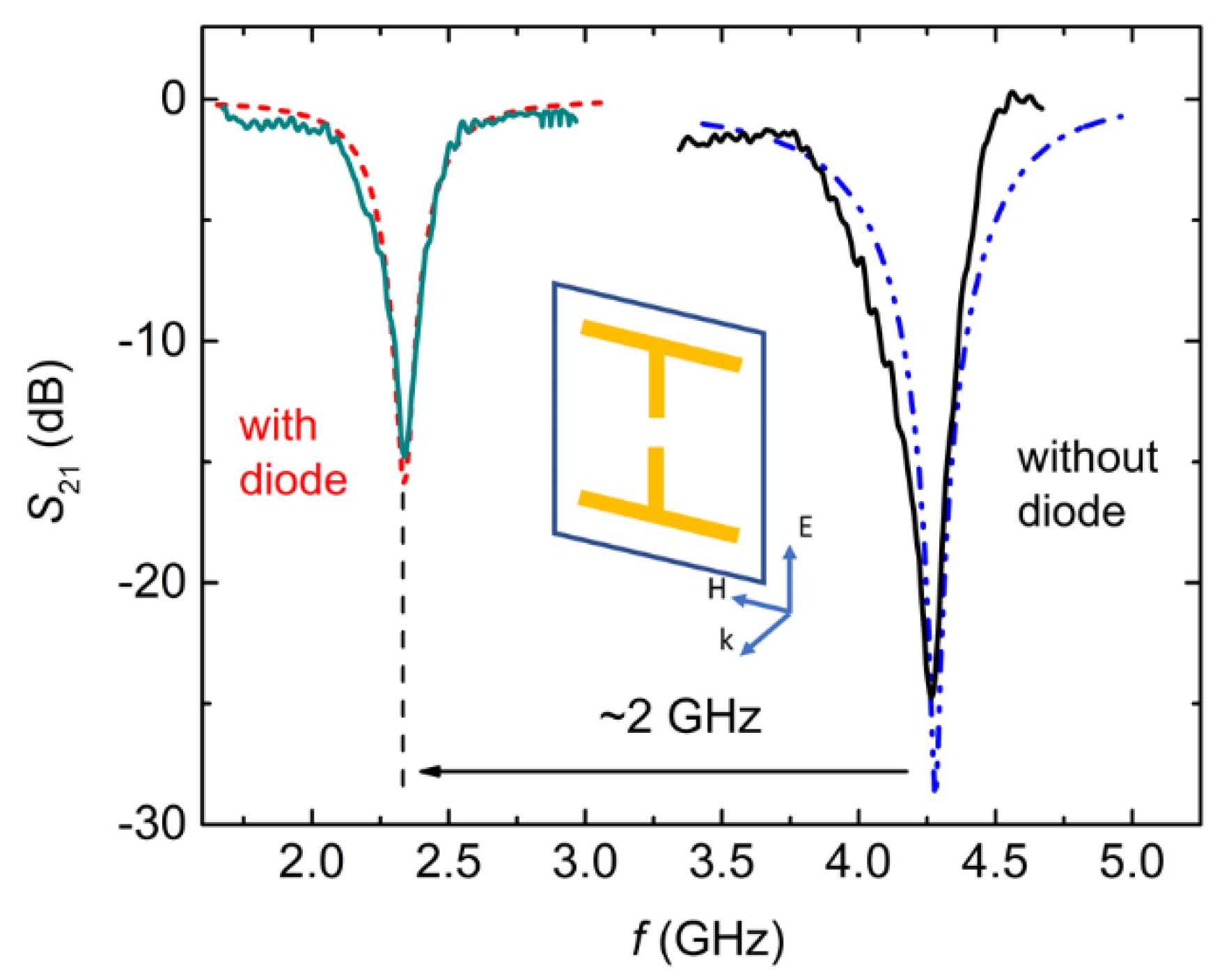
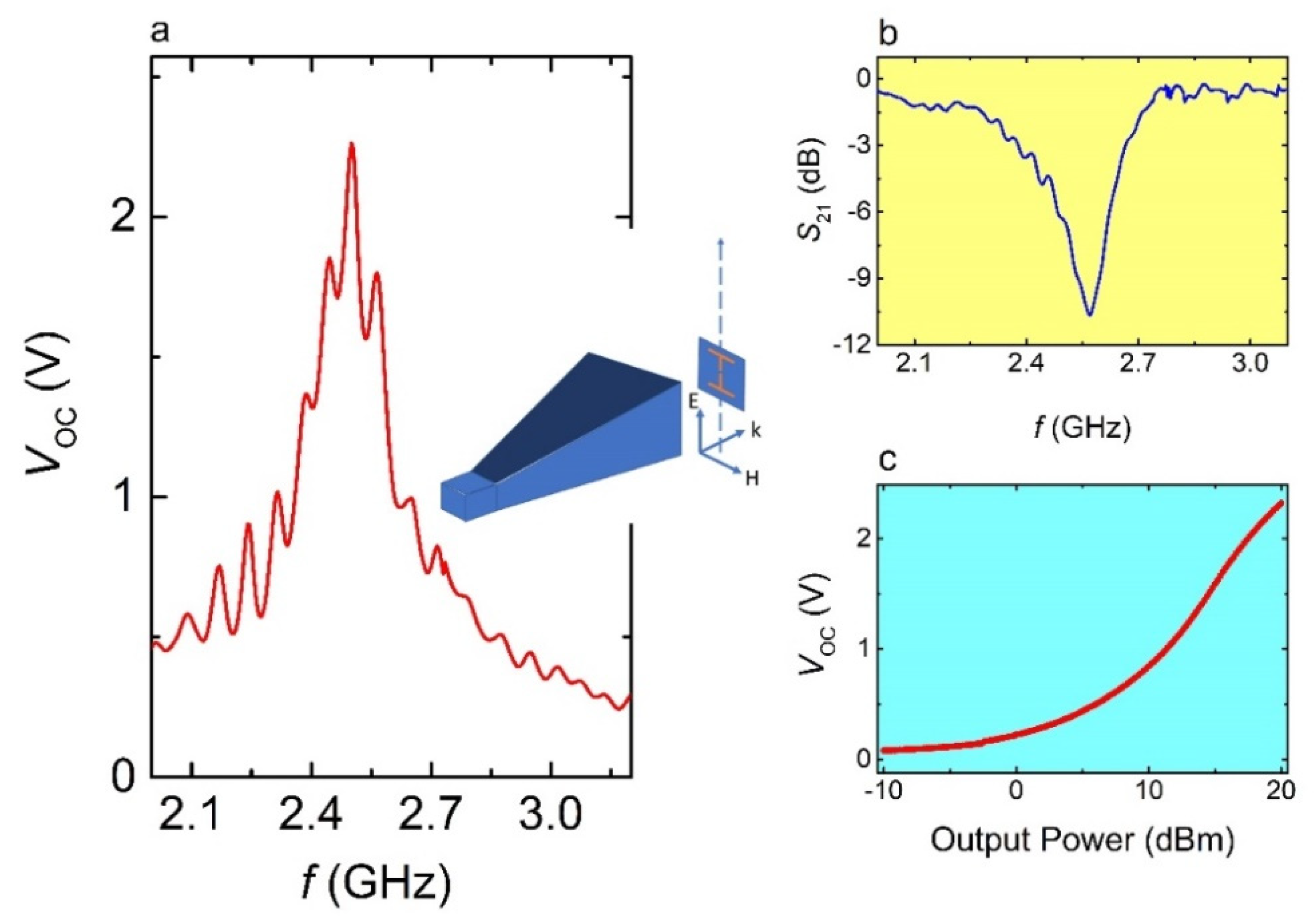
3.1. Electromagnetic Response of the FR-4 Built MS

The EM response of the FR-4 built MS are shown (Figure 2). In particular, the bare MS (no diode included; black solid curve) shows a well-defined transmission dip at 4.3 GHz, suggestive of the meta-atom resonance when the gap is left open acting as a geometric capacitance. When the diode is inserted into the gap and permits a current flow (red curve), the resonance frequency strongly shifts towards a lower frequency regime, i.e., at 2.34 GHz (light green solid line), due to the absence of the geometric capacitance. At the same time, it is getting shallower, however, still strong and well-defined. The Full Width at Half Maximum (FWHM) of the latter transmission dip is 265 MHz, while for the former is ~220 MHz. The ~1.9 GHz shift has been previously reported [18]. The overall EM behavior of the MS (with and without the diode) is consistent with the simulation results (dashed lines, Figure 2).
Interestingly, the 2.34 GHz resonance frequency is very close to the wi-fi frequency (2.4 GHz), and hence, such a MS unit could be a potential candidate for energy harvesting at the wi-fi band. Further EM response measurements have been performed with respect to the direction of the incident wave, for the FR-4 built MS unit, with diode attached into the gap. It is observed that the EM response is hardly affected, as long as the electric field component of the electromagnetic wave keeps parallel to the cut-wire axis, thus exciting the electric dipole resonance (supplementary materials, Figure S1a,b. On the other hand, as the cut-wire axis turns to be perpendicular to E, the resonance becomes less efficiently excited until not at all (supplementary materials, Figure S1c,d. This EM Behavior has been reproduced by the simulations, as well (supplementary materials, Figure S2). Therefore, the MS absorbs energy when the incident electric field is parallel to the cut-wire axis and thus able to excite the electric dipole resonance of the meta-atom.

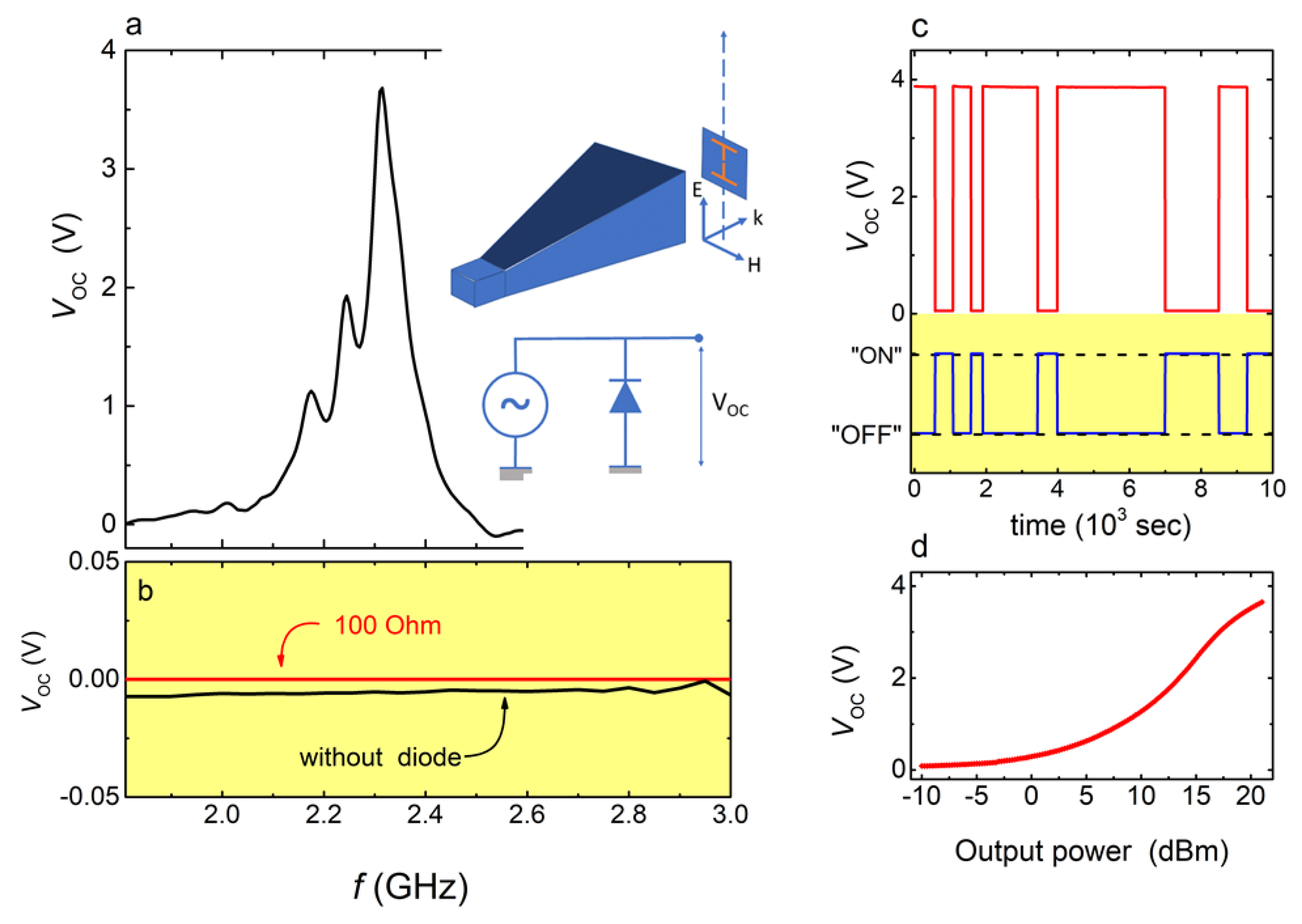
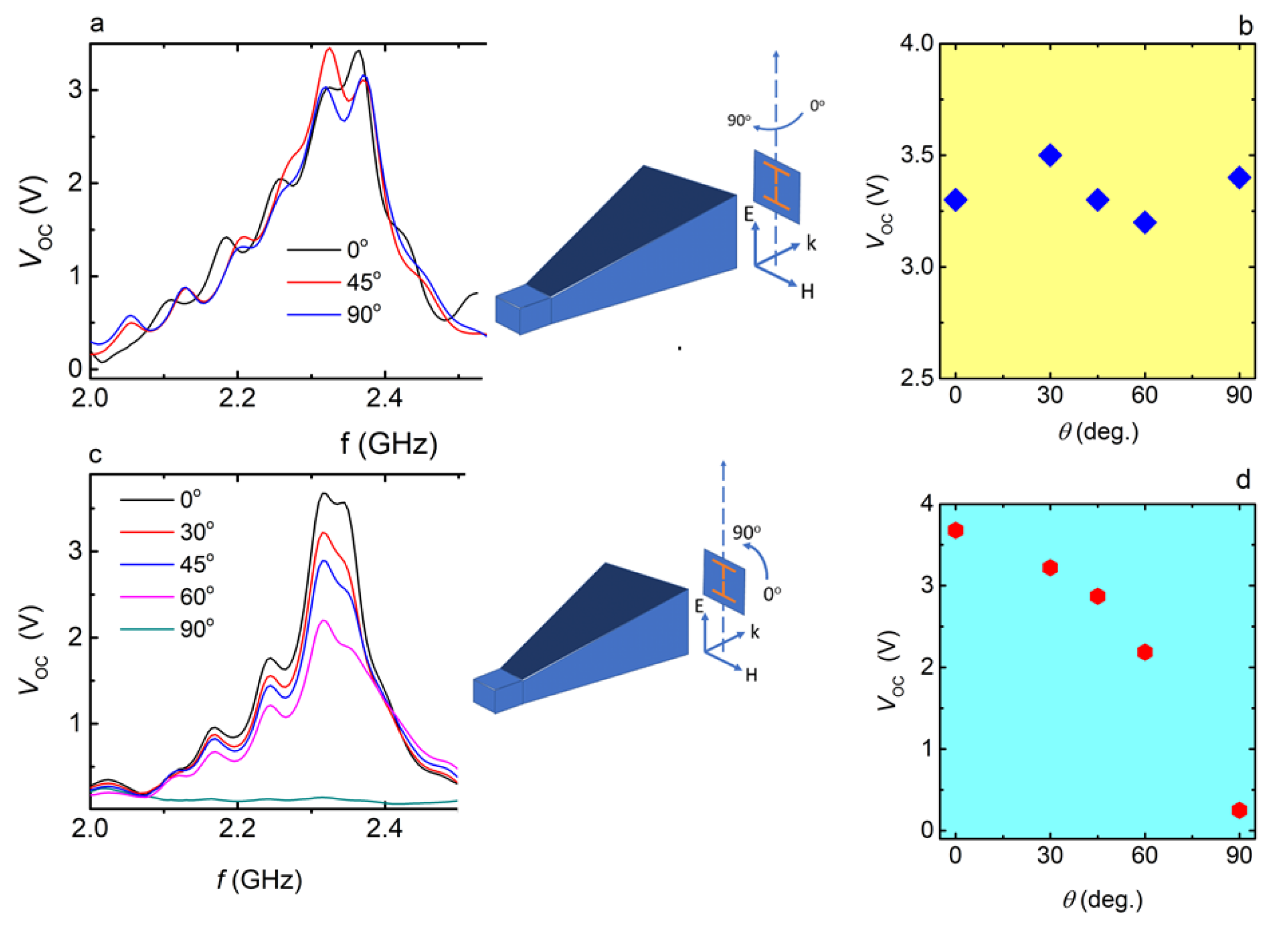
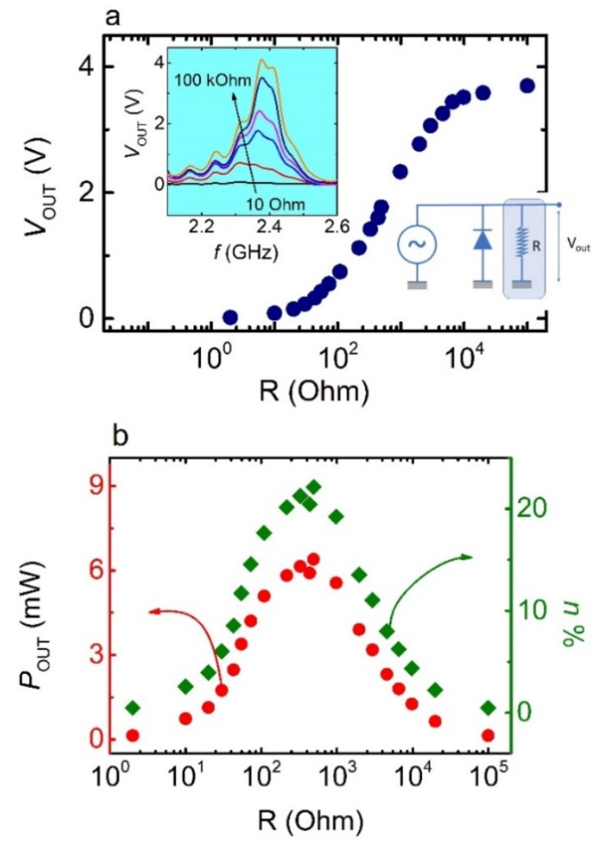
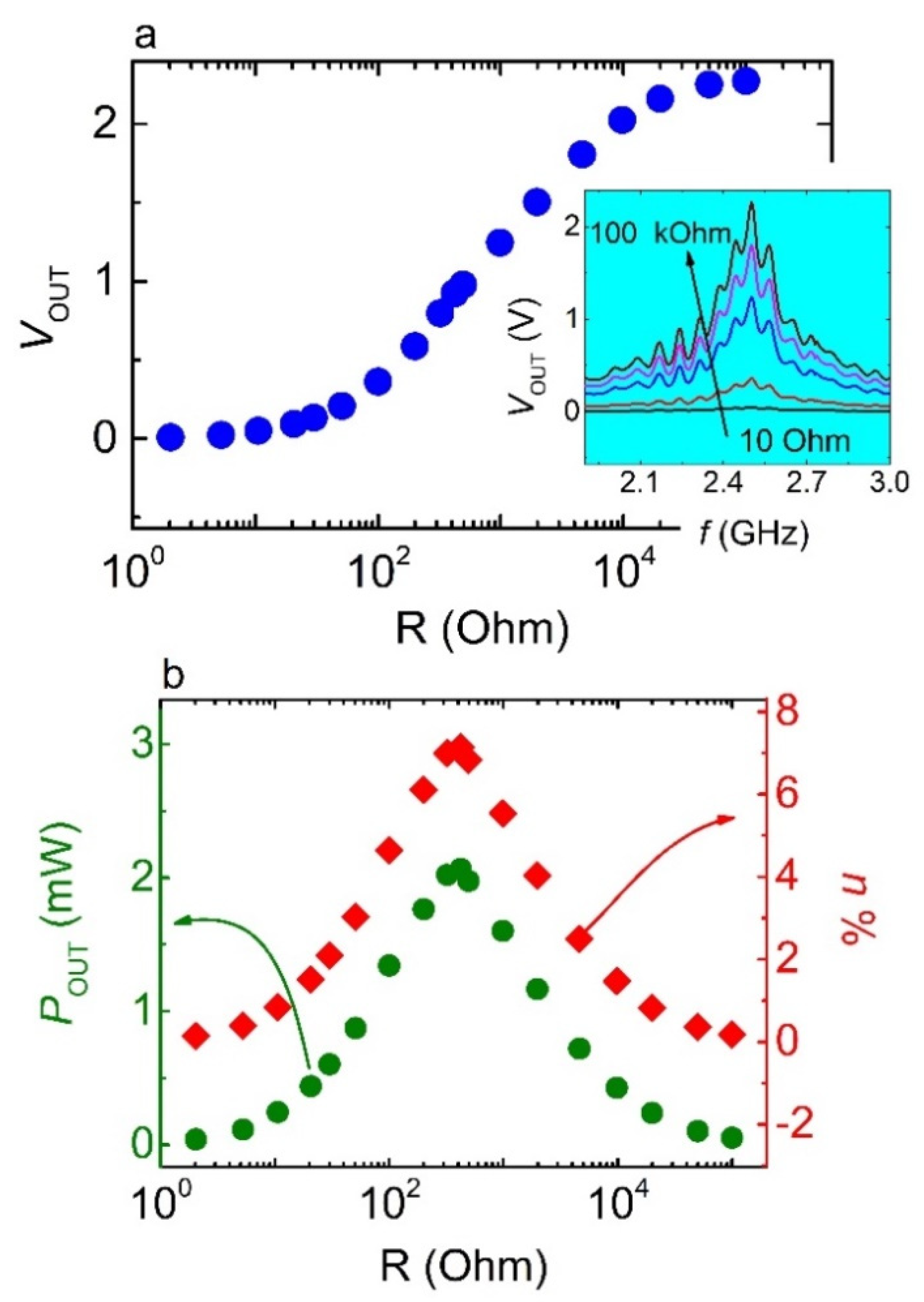
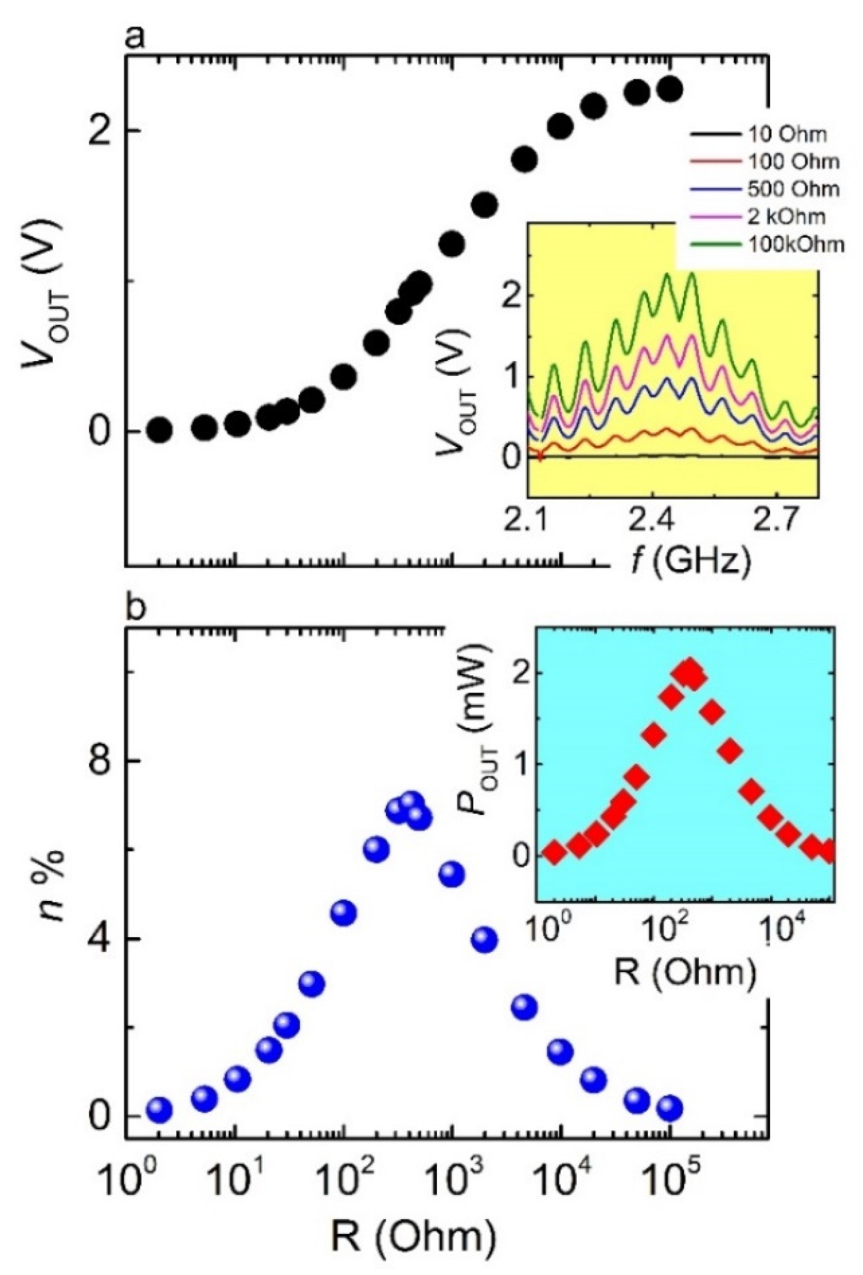
3.2. Verification of Energy Harvesting in FR-4 Built MS

Figure 3a shows the measured open circuit voltage response V OC of the FR-4 built MS, with the E parallel to the cut-wire axis (upper inset, Figure 3a). A broad peak is shown with its maximum at 2.31 GHz, coinciding with the resonance frequency, in Figure 2. The peak value is ~3.5 V, and its FWHM is ~100 MHz. The voltage measured strongly indicates that the MS harvests microwave energy, which is transformed to the DC electric power, through the diode. No other voltage peaks are observed above 2.6 GHz. Below 2.31 GHz, other lower voltage ripples are observed. Here, it must be noted that the diode, as a non-linear electronic element, traps modes of other harmonic frequencies than the fundamental one, in which all of them contribute to the final voltage response, probably enhancing the curvy picture of the voltage.
At this point, additional experiments were performed, to confirm that the measured voltage intrinsically results from the microwave energy harvesting, and it is not an artifact, originating from other external sources, or coming from the experimental set-up itself. Firstly, we measured the voltage response of the MS, without the diode. In this case, zero voltage was detected (black line, Figure 3b) in the whole measured frequency range, indicating that the voltage drop is observed only when the diode is connected to the MS. This is due to the fact that the AC voltage that builds up on the gap needs to be rectified, otherwise the meta-atom acting as an antenna will re-radiate the energy in free space. Secondly, we put a 100 Ohm resistor instead of the diode and repeated the measurement. The diode possesses non-negligible internal resistance and therefore, it is crucial to clarify its possible contribution to microwave signal rectification. Again, zero voltage was recorded (red line, Figure 3b), in the whole frequency range (at least within the resolution of the voltmeter used). As a third test, we put the diode back into the MS and measured the voltage drop against time, at the resonance frequency (2.31 GHz). The measured signal (Figure 3c) is extremely stable, indicating the normal, continuous rectification of the microwave signal, harvested by the MS. Moreover, when the horn power is interrupted (state “OFF”), the measured voltage drops down to zero and it again abruptly increases to the previously measured level, when the horn power sets on (state “ON”). Finally, we measured the open-circuit voltage, at peak frequency, against the output power, that the microwave power generator drives to the horn. The recorded voltage increases with the increasing incident power (Figure 3d). Therefore, it is demonstrated that the measured voltage results from rectification of a microwave signal, which is received by the MS. Consequently, the cut-wire MS harvests microwave energy most effectively at the resonance frequency of 2.31 GHz.
Such an important observation merits further investigation, i.e., it is prudent to study the voltage response of the MS, with respect to the incident wave. In this context, Figure 4a shows the measured open-circuit voltage, as a function of frequency, for several angles θ , as shown in Figure 4b. It must be noted that θ corresponds to the configuration with the MS face in front of the horn, as shown in the inset sketch. It is clearly seen that the voltage peak exhibits values higher than 3 V, regardless of the angle θ . Moreover, the voltage peak position is robust, at ~2.31 GHz. Such constant behaviour matches the corresponding EM response (i.e., supplementary materials Figure S1, panels (a) and (b)). In addition, the voltage response decreases with the increasing angle ϕ (Figure 4c), and is completely eliminated as the MS turns to 90°, with respect to the electric field component of the incident electromagnetic wave (Figure 4d). Such behaviour also agrees with the corresponding EM response (supplementary materials Figure S1, panels (c) and (d).) We stress once more that this behaviour is physically anticipated since the electric dipole resonance of the cut-wire cannot be excited in this case. Therefore, the open circuit voltage behaviour resembles that of the EM response, i.e., V OC remains stable, as long as the electric field keeps parallel to the cut-wire axis. In contrast, V OC decreases as the cut-wire axis turns to become perpendicular to the electric field. From the above experiments, it is evident that the harvesting procedure is maximized when the electric field component of the incident microwave is parallel to the MS orientation.
Since harvesting properties have been demonstrated for the cut-wire metasurface, it becomes crucial to explore its performance. To this point, we study the effect of a resistance load, connected to the device, as shown in the lower inset of Figure 5a. By varying the resistance, the output voltage is measured at resonance frequency and the results are pictured in Figure 5a. The voltage V OUT increases with the increasing R, and reaches the open circuit voltage ( V OC   ~ 3.5   V ) for resistance loads larger than 100 kOhm. Furthermore, the output power can be calculated, using the relation P OUT = V OUT 2 / R and is demonstrated in Figure 5b (red solid circles). It is seen that the maximum output power ( P OUT = 6.4   mW ) is achieved for ~500 Ohm resistance load ( V OUT   ~ 1.77   V ), indicating the optimal performance of the device. The optimum output voltage value is comparable to others, previously reported for metasurface harvesting devices [33]. The resistance value for the optimal performance is analogous to others, which has been used in other microwave harvesting metasurfaces [13,14,16].
To calculate the efficiency of the device, the power received by the MS is required. In the experimental configuration, the MS under the test is placed exactly in front of the horn, and therefore we can treat the horn as an open waveguide. Considering that the signal generator supplies the horn antenna, with a maximum power of 0.68 W, the horn cross section is 212.5 cm2 and the effective area of the MS is 9 cm2. It is easily calculated that the
MS effectively covers the 4.23% of the total horn cross section. Thus, the estimated power received from the MS is P IN = 28.9   mW . The efficiency of the MS harvester is determined using the relation n % = P OUT / P IN . The calculated efficiency as a function of resistance load is shown in Figure 5b (green solid rhombs). Maximum efficiency n = 22.1 % is obtained. This value is lower than others reported, so far [11,13,14,15,16,17,34], while it is comparable to others [12,33]. Note that since the MS is only electrically polarizable (and not artificially magnetically polarizable, as well), impedance matching with free-space cannot be satisfied, the maximum absorption in these cases is 50%. As a result, the maximum harvesting efficiency anticipated for the investigated MS unit is 50%, as shown by the simulations [18]. Therefore, this MS unit is expected to be less efficient than others previously proposed. As mentioned before, we do not use any dedicated rectification circuit, as used in other cases, and that most likely downgrades the harvesting efficiency of the device. In addition, there is no anechoic chamber used in our experiments, and thus more noise is added to the measured signals, reducing further the overall harvesting capability of our device. Considering the above, the obtained efficiency can be denoted as effective.

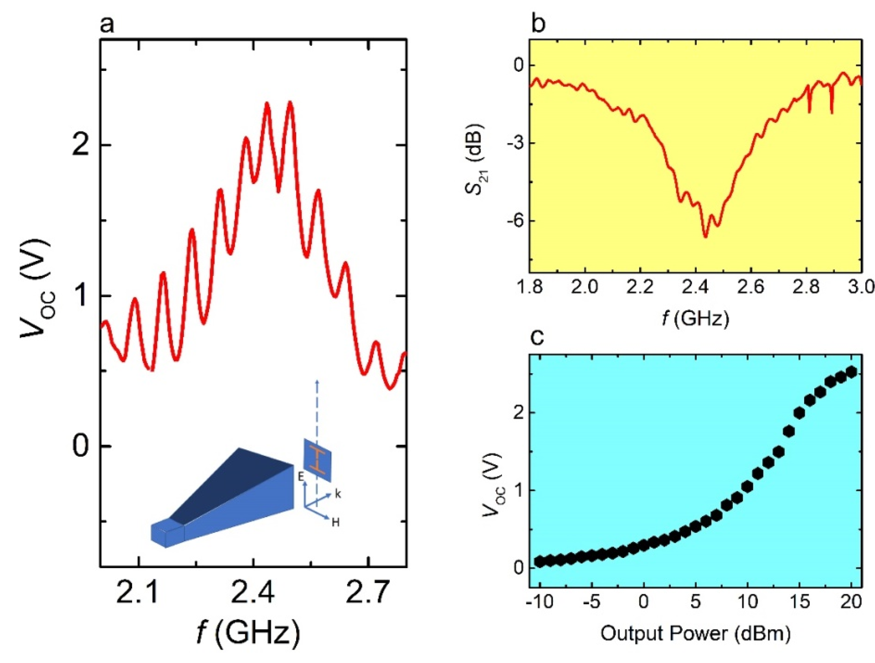
3.3. Verification of Energy Harvesting in Ag/PLA MS

We now turn to the Ag/PLA MS unit measurements. The open circuit voltage VOC as a function of frequency is shown in Figure 6a. A broad peak is observed at ~2.5 GHz, corresponding to the resonance frequency (Figure 6b). The highest voltage value observed is ~2.3 V, which is lower than that obtained for the FR-4 built MS. The peak has a FWHM ~200 MHz, almost the same as the FR-4 MS unit, while there are no other voltage peaks observed below 2 GHz and above 3 GHz, respectively. In addition, the voltage increases with the increasing receiving power, as shown in the inset of Figure 6c. Therefore, it seems that the 3D-printed Ag/PLA MS unit can harvest microwave energy, in the range near 2.4 GHz. Moreover, its harvesting capability is sustainable, regardless of the angle of the MS surface with respect to the incident wave (i.e., supplementary materials, Figure S3a). On the other hand, as the MS turns, with respect to the horizontal axis (E parallel to the cut-wire axis, to E perpendicular to the cut-wire axis, orientation), the output voltage is reduced to zero, indicating that the MS harvests only when the direction of the electric field component of the propagating wave is parallel to the gap (Figure S3b). Both of the abovementioned features corroborate with those obtained for the FR-4 built MS unit, denoting that the overall behaviour of both MS units is qualitatively similar. Figure 7a shows the effect of the resistance load to the output voltage. VOUT increases with the increasing R and reaches the open circuit value (~2.3 V) for resistances larger than ~100 kOhm. However, regardless of the resistance load, VOUT shows a peak at 2.5 GHz (Figure 6a, inset). On the other hand, the output power POUT increases with R, and reaches its peak value (~2.1 mW), for R ~400 Ohm (Figure 7b). For such resistance load, the output voltage is VOUT ~1 V. For higher resistances, POUT decreases. Correspondingly, the maximum efficiency of the Ag/PLA MS is estimated n %   ~ 7 % , which is 3 times lower than that obtained for the FR-4 built MS. Therefore, the 3D-printed Ag/PLA MS harvests less efficiently than the FR-4 built MS.

3.4. Verification of energy Harvesting in Electrifi MS

Finally, we investigate the harvesting performance of the Electrifi MS unit. The open circuit voltage as a function of frequency is shown in Figure 8a. A broad peak is observed, with its centre at 2.4 GHz. Notably, at the same frequency, the EM response of the MS unit exhibits a local minimum, indicative of resonance (Figure 8b). The highest voltage value observed is ~2 V, which is almost identical to that obtained from the Ag/PLA MS unit. The peak is relatively narrow (FWHM ~200 MHz), while there are no other voltage peaks observed below 2 GHz and above 3 GHz, respectively. In addition, the voltage increases with the increasing receiving power, as shown in the inset of Figure 8c. Furthermore, the open circuit voltage observed in the Electrifi MS unit remains almost unaffected, as long as the electric field component of the incident wave is parallel to the gap. On the other hand, it is minimized when the magnetic field of the incident wave is parallel to the gap (not shown here). Consequently, the Electrifi MS unit harvests in the same manner with the Ag/PLA MS unit.
Figure 9a shows the output voltage as a function of resistance load. V OUT increases with the increasing R, and reaches the open circuit value V OC for resistance higher than ~50 KOhm. Nevertheless, the maximum power output is obtained for R ~400 Ohm, as shown in Figure 9b, inset. The maximum power value is ~2 mW and corresponds to an efficiency of ~7% (main panel, Figure 9b). The efficiency determined for the Electrifi MS unit equals that obtained for the Ag/PLA MS, suggesting their equal (qualitative and quantitative) performance.

4. Summary

In the current study, cut-wire metasurface units were constructed employing the Fused Filament Fabrication 3D-printing method. The MSs constructed hereby were tested regarding their efficiency in microwave energy harvesting in the 2.4 GHz frequency band. Their performance was compared to a conventionally-built Copper MS unit on a FR-4, which is a widely used substrate in microwave applications.
In this context, the FR-4 built MS was initially investigated. The MS shows resonance at ~2.3 GHz. The observed EM behavior of the MS has been corroborated by theoretical simulation results.
By placing the MS unit in front of a horn antenna, which emits electromagnetic waves, the MS harvests energy and transforms it to a DC voltage, through the Schottky diode, attached into the gap. The measured open circuit voltage is maximized (~3 V) around the resonance frequency, i.e., 2.3 GHz, and is constant with respect to time. Moreover, it is minimized as soon as the emitted electromagnetic wave is turned off as well as gradually increases with the increasing horn output power. Furthermore, the FR-4 built MS unit harvests energy, when the electric field remains parallel to the MS gap. By attaching an external resistance load of ~500 Ohm, the MS maximizes its output power, leading to an efficiency of ~22%. Such value is half of the efficieny estimated, by theoretical calculations for this MS unit. On the other hand, it is comparable to efficiencies reported for other microwave energy harvesters.
Following the same route, the harvesting efficiency of Ag-painted PLA as well as Electricfi MS units, is investigated. Both of them exhibit harvesting behaviour, very similar to the behaviour of the FR-4 MS unit. The obtained open circuit voltage is slightly lower (~2 V), however, it is observed in the frequency range around 2.4 GHz.
Therefore, both 3D printed MS units can harvest in the 2.4 GHz frequency band. Moreover, by connecting an external resistance of 400 Ohm both Ag/PLA and Electrifi MSs show maximum power output (~2.5 mW), resulting in a moderate efficiency of ~7%. Such efficiency is three times lower than that obtained for the FR-4 built MS unit.

5. Conclusions

The efficiency of the 3D-printed metasurfaces presented hereby, is rather low compared to the other metasurfaces conventionally constructed and reported, so far. Such metasurfaces exhibit low electrical conductivity, which mainly contributes to their suppressed harvesting performance.
However, such a low efficiency, in some cases, could be counter balanced by the distinctive advantages of the 3D-printed metasurfaces, i.e., their cheap, quick, multi-material, cost-effective, and user-friendly construction. Therefore, the overall performance of both Ag/PLA and Electrifi metasurfaces evidently suggests that 3D-printed metasurfaces could be potentially used for energy harvesting applications.

Supplementary Materials

The following are available online at https://www.mdpi.com/article/10.3390/cryst11091089/s1, Figure S1: Electromagnetic response of the FR-4 built MS, with repsect to polarization angles, Figure S2: Simulations for the FR-4 built MS, with respect to polarization angles, Figure S3: Output voltage, with respect to polarization angles, for the Ag/PLA MS.

Author Contributions

Conceptualization and methodology, Z.V., E.N.E. and G.K.; bibliographic investigation, E.T., Z.V. and G.K.; experimental synthesis and characterization, E.T., Z.V. and G.K.; data analysis, Z.V., E.T. and G.K.; theoretical simulations, O.T. and A.C.T.; funding acquisition, G.K. All authors have read and agreed to the published version of the manuscript.

Funding

This research has been co-financed by the European Union and Greek national funds through the Operational Program Competitiveness, Entrepreneurship and Innovation, under the call RESEARCH–CREATE–INNOVATE; project code: T1EDK-02784; acronym: POLYSHIELD; project code: T2EDK-02073; acronym: SEMI-WEB.

Data Availability Statement

All the data reported here can be made available on request.

Conflicts of Interest

The authors declare no conflict of interest.

References

  1. Soukoulis, C.M.; Wegener, M. Past achievements and future challenges in the development of three-dimensional photonic metamaterials. Nat. Photonics 2011, 5, 523–530. [Google Scholar] [CrossRef] [Green Version]
  2. Bukhari, S.S.; Vardaxoglou, J.Y.; Whittow, W. A Metasurfaces Review: Definitions and Applications. Appl. Sci. 2019, 9, 2727. [Google Scholar] [CrossRef] [Green Version]
  3. Chen, T.; Li, S.; Sun, H. Metamaterials application in sensing. Sensors 2012, 12, 2742–2765. [Google Scholar] [CrossRef]
  4. Choudhary, Y.S.; Gomathi, N. Advanced Materials for Electromagnetic Shielding Metamaterials as Shielding Materials. In Advanced Materials for Electromagnetic Shielding: Fundamantals, Properties and Appplications; Jaroszewski, M., Thomas, S., Rane, A.V., Eds.; Wiley: Hoboken, NJ, USA, 2018; pp. 367–391. [Google Scholar] [CrossRef]
  5. Xing, X.; Li, Y.; Lu, Y.; Zhang, W.; Zhang, X.; Han, J.; Zhang, W. Terahertz metamaterial beam splitters based on untraditional coding scheme. Opt. Express 2019, 27, A1627–A1635. [Google Scholar] [CrossRef] [PubMed]
  6. Tsilipakos, O.; Xomalis, A.; Kenanakis, G.; Farsari, M.; Soukoulis, C.M.; Economou, E.N.; Kafesaki, M. Split-cube-resonator-based metamaterials for polarization-selective asymmetric perfect absorption. Sci. Rep. 2020, 10, 17653. [Google Scholar] [CrossRef] [PubMed]
  7. Tsilipakos, O.; Zhang, L.; Kafesaki, M.; Soukoulis, C.M.; Koschny, T. Experimental Implementation of Achromatic Multiresonant Metasurface for Broadband Pulse Delay. ACS Photonics 2021, 8, 1649–1655. [Google Scholar] [CrossRef]
  8. Chen, Z.; Guo, B.; Yang, Y.; Cheng, C. Metamaterials-based enhanced energy harvesting: A review. Phys. B Condens. Matter 2014, 438, 1–8. [Google Scholar] [CrossRef]
  9. Shaikh, F.K.; Zeadally, S. Energy harvesting in wireless sensor networks: A comprehensive review. Renew. Sustain. Energy Rev. 2016, 55, 1041–1054. [Google Scholar] [CrossRef]
  10. Tan, T.; Yan, Z.; Zou, H.; Ma, K.; Liu, F.; Zhao, L.; Peng, Z.; Zhang, W. Renewable energy harvesting and absorbing via multi-scale metamaterial systems for Internet of things. Appl. Energy 2019, 254, 113717. [Google Scholar] [CrossRef]
  11. Ramahi, O.M.; Almoneef, T.S.; AlShareef, M.; Boybay, M.S. Metamaterial particles for electromagnetic energy harvesting. Appl. Phys. Lett. 2012, 101, 173903. [Google Scholar] [CrossRef] [Green Version]
  12. Hawkes, A.M.; Katko, A.R.; Cummer, S.A. A microwave metamaterial with integrated power harvesting functionality. Appl. Phys. Lett. 2013, 103, 163901. [Google Scholar] [CrossRef] [Green Version]
  13. El Badawe, M.; Almoneef, T.S.; Ramahi, O.M. A metasurface for conversion of electromagnetic radiation to DC. AIP Adv. 2017, 7, 35112. [Google Scholar] [CrossRef] [Green Version]
  14. Duan, X.; Chen, X.; Zhou, L. A metamaterial electromagnetic energy rectifying surface with high harvesting efficiency. AIP Adv. 2016, 6, 125020. [Google Scholar] [CrossRef]
  15. Almoneef, T.S.; Ramahi, O.M. Metamaterial electromagnetic energy harvester with near unity efficiency. Appl. Phys. Lett. 2015, 106, 153902. [Google Scholar] [CrossRef]
  16. Almoneef, T.S.; Erkmen, F.; Ramahi, O.M. Harvesting the Energy of Multi-Polarized Electromagnetic Waves. Sci. Rep. 2017, 7, 14656. [Google Scholar] [CrossRef] [PubMed] [Green Version]
  17. Aldhaeebi, M.A.; Almoneef, T.S. Planar Dual Polarized Metasurface Array for Microwave Energy Harvesting. Electronics 2020, 9, 1985. [Google Scholar] [CrossRef]
  18. Oumbé Tékam, G.T.; Ginis, V.; Danckaert, J.; Tassin, P. Designing an efficient rectifying cut-wire metasurface for electromagnetic energy harvesting. Appl. Phys. Lett. 2017, 110, 83901. [Google Scholar] [CrossRef] [Green Version]
  19. Erkmen, F.; Ramahi, O.M. A Scalable, Dual-Polarized Absorber Surface for Electromagnetic Energy Harvesting and Wireless Power Transfer. IEEE Trans. Microw. Theory Tech. 2021, 69, 4021–4028. [Google Scholar] [CrossRef]
  20. Ashoor, A.Z.; Ramahi, O.M. Polarization-Independent Cross-Dipole Energy Harvesting Surface. IEEE Trans. Microw. Theory Tech. 2019, 67, 1130–1137. [Google Scholar] [CrossRef]
  21. Nowak, M. Metamaterial-Based Sub-Microwave Electromagnetic Field Energy Harvesting System. Energies 2021, 14, 3370. [Google Scholar] [CrossRef]
  22. Wagih, M.; Weddell, A.S.; Beeby, S. Rectennas for Radio-Frequency Energy Harvesting and Wireless Power Transfer: A Review of Antenna Design [Antenna Applications Corner]. IEEE Antennas Propag. Mag. 2020, 62, 95–107. [Google Scholar] [CrossRef]
  23. Shahrubudin, N.; Lee, T.C.; Ramlan, R. An Overview on 3D Printing Technology: Technological, Materials, and Applications. Procedia Manuf. 2019, 35, 1286–1296. [Google Scholar] [CrossRef]
  24. Ngo, T.D.; Kashani, A.; Imbalzano, G.; Nguyen, K.T.Q.; Hui, D. Additive manufacturing (3D printing): A review of materials, methods, applications and challenges. Compos. Part B Eng. 2018, 143, 172–196. [Google Scholar] [CrossRef]
  25. Vallecchi, A.; Cadman, D.; Whittow, W.G.; Vardaxoglou, J.; Shamonina, E.; Stevens, C.J. 3-D Printed Bandpass Filters with Coupled Vertically Extruded Split Ring Resonators. IEEE Trans. Microw. Theory Tech. 2019, 67, 4341–4352. [Google Scholar] [CrossRef] [Green Version]
  26. Salim, A.; Ghosh, S.; Lim, S. Low-Cost and Lightweight 3D-Printed Split-Ring Resonator for Chemical Sensing Applications. Sensors 2018, 18, 3049. [Google Scholar] [CrossRef] [PubMed] [Green Version]
  27. Tasolamprou, A.C.; Mentzaki, D.; Viskadourakis, Z.; Economou, E.N.; Kafesaki, M.; Kenanakis, G. Flexible 3D Printed Conductive Metamaterial Units for Electromagnetic Applications in Microwaves. Materials 2020, 13, 3879. [Google Scholar] [CrossRef]
  28. Pizarro, F.; Salazar, R.; Rajo-Iglesias, E.; Rodríguez, M.; Fingerhuth, S.; Hermosilla, G. Parametric Study of 3D Additive Printing Parameters Using Conductive Filaments on Microwave Topologies. IEEE Access 2019, 7, 106814–106823. [Google Scholar] [CrossRef]
  29. Ishikawa, A.; Kato, T.; Takeyasu, N.; Fujimori, K.; Tsuruta, K. Selective electroless plating of 3D-printed plastic structures for three-dimensional microwave metamaterials. Appl. Phys. Lett. 2017, 111, 183102. [Google Scholar] [CrossRef]
  30. Kenanakis, G.; Vasilopoulos, K.C.; Viskadourakis, Z.; Barkoula, N.-M.; Anastasiadis, S.H.; Kafesaki, M.; Economou, E.N.; Soukoulis, C.M. Electromagnetic shielding effectiveness and mechanical properties of graphite-based polymeric films. Appl. Phys. A 2016, 122, 802. [Google Scholar] [CrossRef]
  31. Mousa Ali, E.; Yahaya, N.Z.; Nallagownden, P.; Zakariya, M.A. A novel rectifying circuit for microwave power harvesting system. Int. J. RF Microw. Comput. Eng. 2017, 27, e21083. [Google Scholar] [CrossRef]
  32. Wang, D.; Negra, R. Design of a rectifier for 2.45 GHz wireless power transmission. In Proceedings of the PRIME 2012 8th Conference on Ph.D. Research in Microelectronics & Electronics, Aachen, Germany, 12–15 June 2012; pp. 1–4. [Google Scholar]
  33. Wang, R.; Ye, D.; Dong, S.; Peng, Z.; Salamin, Y.; Shen, F.; Huangfu, J.; Li, C.; Ran, L. Optimal Matched Rectifying Surface for Space Solar Power Satellite Applications. IEEE Trans. Microw. Theory Tech. 2014, 62, 1080–1089. [Google Scholar] [CrossRef]
  34. Ghaderi, B.; Nayyeri, V.; Soleimani, M.; Ramahi, O.M. Pixelated Metasurface for Dual-Band and Multi-Polarization Electromagnetic Energy Harvesting. Sci. Rep. 2018, 8, 13227. [Google Scholar] [CrossRef] [PubMed]
Figure 1. (a) FR-4 based metasurface (MS) units are demonstrated in the lower part of the picture. PLA (as-prepared) and Electrifi T-like, 3D printed components are shown above the FR-4 MS; (b) PLA/Ag and the Electrifi cut-wire MSs, used for energy harvesting experiments. The Schottky diode is clearly seen inside the MS gap; (c) dimensions of the MS unit; (d) experimental configuration, used for energy harvesting experiments.
Crystals 11 01089 g001
Figure 2. Electromagnetic (EM) response of the FR-4 built metasurface (MS), with diode included into the MS gap (green solid line) and without diode (black solid line). The dashed lines correspond to the results as derived through theoretical simulations. The inset sketch shows the orientation of the MS, with respect to the incident wave.
Crystals 11 01089 g002
Figure 3. (a) Open circuit voltage V OC as a function of frequency f, for the FR-4 based MS (with diode, placed into the gap). The orientation of the MS, with respect to the horn is pictured in the included sketch (inset). The corresponding electronic circuit, is demonstrated, in the lower sketch. The AC voltage source equals the MS unit, which harvests energy; (b) V OC vs. f, for the same MS, without diode (black solid line) and with a resistor placed into the gap, instead of the diode (red solid line); (c) V OC vs. time (red solid line). The voltage value is zero when the horn power is OFF (blue solid line), while it is non-zero when horn power is ON. The stability of the voltage signal is obviously seen; (d) V OC as a function of the horn output power.
Crystals 11 01089 g003
Figure 4. (a) Open circuit voltage as a function of frequency, for various θ = 0 ° (black line), θ = 45 ° (red line), and θ = 90 ° (blue line). The sketch shows the corresponding experimental configuration; (b) maximum open circuit voltage vs. angle θ ; (c) open circuit voltage as a function of frequency, for several ϕ angles. The sketch shows the corresponding experimental configuration; (d) maximum open circuit voltage vs. angle ϕ , as extracted from the main panel.
Crystals 11 01089 g004
Figure 5. (a) Output voltage vs. resistance load. The equivalent electronic circuit is pictured in the right sketch. The AC power supply stands for the MS unit, which receives the microwave energy. The connected resistance is highlighted. Blue inset. VOUT vs. f for selected resistance loads. All of the curves exhibit maximum value at resonance frequency (2.32 GHz). The equivalent electronic circuit is pictured in the inset; (b) output power as a function of resistnace load (red solid circles) and efficiency vs. resistance (green solid rhombs). A clear maximum is obtained for ~500 Ohm.
Crystals 11 01089 g005
Figure 6. (a) Open circuit voltage VOC vs. f, for the Ag/PLA MS unit. The experimental configuration is shown in the sketch; (b) EMI response of the MS unit, with diode attached to the MS gap; (c) VOC as a function of the horn output power.
Crystals 11 01089 g006
Figure 7. (a) Output voltage vs. resistance load, for the Ag/PLA MS, blue inset. Output voltage as a function of frequency for selected resistance loads, i.e., 5 Ohm (black line), 100 Ohm (red line), 500 Ohm (blue line), 5 kOhm (magenda line), and 100 kOhm (dark green line); (b) output power as a function of resistance load (green circles) and efficiency vs. resistance (red rhombs). A clear maximum is obtained for R ~400 Ohm.
Crystals 11 01089 g007
Figure 8. (a) Open circuit voltage VOC vs. f, for the Electrifi MS unit. The experimental configuration is shown in the sketch; (b) EMI response of the Electrifi MS unit, with diode attached to the MS gap; (c) VOC as a function of the horn output power.
Crystals 11 01089 g008
Figure 9. (a) Output voltage vs. resistance load, for the Electrifi MS, yellow inset: V OUT as a function of frequency for the selected resistance loads; (b) MS harvesting efficiency as a function of resistance load. A clear maximum is obtained for R ~400 Ohm, blue inset: P OUT as a function of R. Local maximum appears for R ~400 Ohm.
Crystals 11 01089 g009
Table 1. Dimensions of the metasurface unit, as shown in Figure 1c.
DimensionValue (mm)
ax, ay30.0
L123.1
L222.8
w1.6
d3.0
Publisher’s Note: MDPI stays neutral with regard to jurisdictional claims in published maps and institutional affiliations.

