Abstract
The historical bottleneck for truly high scale integrated photonics is the light emitter. The lack of monolithically integrable light sources increases costs and reduces scalability. Quantum phenomena found in embedded Si particles in the nanometer scale is a way of overcoming the limitations for bulk Si to emit light. Integrable light sources based in Si nanoparticles can be obtained by different CMOS (Complementary Metal Oxide Semiconductor) -compatible materials and techniques. Such materials in combination with Si3N4 photonic elements allow for integrated Si photonics, in which photodetectors can also be included directly in standard Si wafers, taking advantage of the emission in the visible range by the embedded Si nanocrystals/nanoparticles. We present the advances and perspectives on seamless monolithic integration of CMOS-compatible visible light emitters, photonic elements, and photodetectors, which are shown to be viable and promising well within the technological limits imposed by standard fabrication methods.
1. Introduction
Integrated photonics [1,2,3,4] have an ever-increasing relevance from communications to sensing. While much improvement has been achieved regarding passive and active optical light-guiding elements, the historical bottleneck for truly high scale Photonic Integrated Circuits (PICs) has been the lack of an easily integrable light source. The need for either coupling external emitters [5] or for heterogeneous integration of non-MOS compatible light sources [6] is a significant disadvantage in the regard of cost and scalability.
Embedded nanocrystals (ncs) [7,8,9] and nanoparticles (nps) [10,11,12] represent exciting possibilities for integrated light emitters due to the quantum phenomena observed at nanometric scale, overcoming the main impediment for Si-based light emitting devices: its indirect bandgap characteristics when in bulk.
The observation of PL at room temperature in porous Si by Canham is widely considered as the first sight of possible light generation in such material for further integration with electronics [13,14]. This triggered the study of a variety of nanometric Si-based materials in pursue of better chemical and structural stability, CMOS-compatible fabrication process, and control of the characteristics of the emitted light [15,16,17]. One of the most promising compliant materials is the Silicon Rich Silicon Oxide (SRO). This is a SiOx with 0 < x < 2, in which, after a specific thermal treatment, the silicon atoms not forming dioxide can nucleate to obtain embedded Si-nps [10,18].
The demonstration of Light Emitter Capacitors based on SRO promised the viability of monolithically integrated light emitter using CMOS compatible materials and processes [6,7,19,20,21,22]. The further demonstration of emission enhancement by combining SRO and Si3N4 [17,23,24] was a step forward which, in addition, opened the door for seam-less coupling of light emitters and waveguides in the same process on standard Si substrates [25], dramatically reducing costs and increasing scalability.
To further advance on this matter, it is necessary to understand the balance between the benefits and disadvantages this novel and exciting technology. The viability of optical components is ascribed to the fabrication limits, such as a reduced variety of materials, maximum thicknesses achievable by standard procedures, lithographic resolution, etc. The characteristics of the light produced by the nanoparticles-based light emitters is also an important matter to consider, as it can significantly differ from the light produced by externally coupled lasers, which currently dominate the integrated photonics field. Finally, integrable light detectors must also be analyzed or designed in order to accommodate the architecture, materials and light characteristics.
In this work, we examine the perspective of a fully integrated electrophotonic Si-based platform with directly embedded light sources based on Si nanoparticles. We briefly review the current advances on the development of discrete elements necessary for an SRO\Si3N4 integrated photonics platform, and, along with the proposal of previously unreported results, we analyze them from a holistic point of view, taking into consideration the intricate interrelation between light emitters, passive photonic elements, and available light sensing schemes to assess the viability of monolithic integration using standard CMOS.
2. Materials and Methods
All the materials and devices here analyzed were obtained using standard CMOS processes and standard crystalline Si wafers as substrate. The active materials and photonic elements are based in SiO2, Si3N4, polycrystalline Si, and Al.
The SRO and SRO-Si3N4 films were fabricated using Low Pressure Chemical Vapor Deposition (LPCVD) with silane and nitrous oxide as precursor gases, and Ionic Implantation (II) of Plasma Enhanced Chemical Vapor Deposition (PECVD) SiO2. Details on temperatures, pressures, gas flows, II energies and doses, and thermal treatments, as well as characterization experimental details, can be found in References [9,10,26,27,28,29].
Details on the fabrication and characterization of electroluminescent devices with polished and unpolished substrates, can be found in References [16,24,30,31], except for the texturization of substrates obtained using the Metal Assisted Chemical Etching (MACE) technique, which is described in References [32,33].
The fabrication and characterization details on the monolithic emitter-waveguide-detector systems can be found in References [25,34].
The simulation of the passive photonic elements was performed using the tools provided by the software Lumerical (Vancouver, BC, Canada). Mode and field propagation simulations were performed using Mode and FDTD. The S-parameters were extracted from these to calculate losses by means of Interconnect. The refractive index of the silicon nitride was the one measured by ellipsometry from samples deposited by LPCVD, which were consistent to Palik data from Lumerical. The simulation domains were delimited by perfectly matched layers (PML) in around the cladding limits.
The simulation of the fabrication process of the waveguided sensor was done using the software Silvaco-Athena (Santa Clara, CA, USA), accounting for all the steps needed to obtain nanoparticle-based emitters using II-SRO, including thermal treatments as described in Reference [24]. Its electro-optical response was simulated using Silvaco-Atlas (Santa Clara, CA, USA), applying 0 V to source and substrate and 5 V in the gate.
3. Luminescence from Nanoparticles in a Dioxide Matrix: SRO
As mentioned, one of the most successful materials containing light-emitting silicon nanoparticles is SRO. It can be fabricated using a variety of CMOS-compatible techniques, of which Low Pressure Chemical Vapor Deposition (LPCVD-SRO), Plasma Enhanced Chemical Vapor Deposition (PECVD-SRO), and Si Ion Implantation into SiO2 (II-SRO) matrices stand out due to their technical simplicity and light emission characteristics [16,26,35].
During the fabrication process of the SRO films, different parameters can be controlled to modify the atomic Si contents in the material. For LPCVD-SRO, the defining parameter is the partial pressures ratio (R0 = PN2O/PSiH2) from precursor gasses flow [16], and for II-SRO the Si-ion implantation dose. The posterior thermal annealing can also be tuned for optimal Si-nucleation and consequent nps size and density in order to obtain optimal light emission [10,36]. In addition, the use of multiple layers of SRO with different characteristics, or silicon nitrides stacked to the main active material, can influence the final emission spectra, as well as the conductivity of the stack structure. Despite the material being intended as part of an electronic device, hence, its emission will be electrically stimulated (Electroluminescence, EL), Photoluminescence (PL) characterization is a powerful tool to understand the emission mechanisms and characteristics in the material, which are fundamentally the same as those for EL [24]. In PL, the emission is stimulated pumping higher energy light (usually ultraviolet for SRO) for photons to be re-emitted with lower energies (in the visible range for SRO). Figure 1 shows examples of PL emission spectra for various SRO and SRO\Si3N4 films when being pumped with UV light. Table 1 summarizes the main characteristics of the emission for active materials with different fabrication parameters. Note that the required times and temperatures by the SRO annealing, while fully available in most CMOS lines, are generally larger than those used for regular processes, such as dopant diffusion or thermal oxidation. Nevertheless, it has been shown that, if the fabrication sequence is adequately planned, the influence by SRO fabrication on electronic circuits, as well as by circuitry fabrication on SRO, are both null [37]. Detailed studies regarding the origin of light emission in SRO can be found in References [9,10,26,27,28,29].
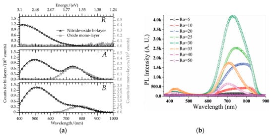
Figure 1.
(a) PL spectra of II-SRO and II-SRO/Si3N4 films [38]; (b) LPCVD-SRO films with different precursors gas ratios, R0 [28].

Table 1.
Fabrication parameters and characteristics of different SRO films.
As mentioned, in the frame of an electronically-driven PICs, the stimuli to the emitting material are expected to be electrical, and, while the physical phenomena concerning light emission are fundamentally the same for EL and PL, other aspects, such as electronic transport and efficiency, must be considered for integrated EL devices [35], as well as the stimuli of different radiation centers in distinct proportions [21]. When characterizing EL, the need for an electrode on top of the SRO is an added difficulty, which, in the case of external light characterization, it must be conductive, while, at the same time, allow light transmission. Highly doped polysilicon is often the material of choice for this, due to its compatibility with standard CMOS, and its acceptable transmittance characteristics [24]. This results in a Light Emitting Capacitor (LEC) configuration as the one exemplified in Figure 2. In this particular case, a Si3N4 layer between SRO and electrode is included, as it has been observed to improve efficiency and emission spectrum [17,23,24]. Figure 3 shows examples of EL emission spectra and images of LECs with single SRO layers (a) and with Silicon Nitride-SRO bi-layers (b). When obtaining external EL spectra, optical effects caused by the multi-layer configuration and transmittance characteristics of the electrode material must be considered in the analyses [39].

Figure 2.
Light Emitting Capacitor stack structure based on SRO/Si3N4 bi-layers (not on scale) [24].
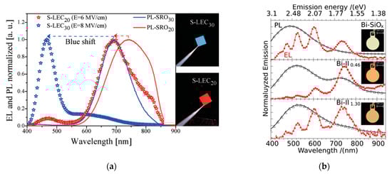
Figure 3.
(a) Micrographs and EL spectra of LPCVD-SRO LECs [16]; (b) II-SRO/Si3N4 LECs [24].
Other mono-layer and stack structure configuration have been more recently proposed with aims to improve emission efficiency, such as single SRO layers, multilayers of SRO with different content of silicon, and two types of Si substrates, by using polished or textured surface [30,31].
In general, the EL spectra extend from blue to near infrared, with two mean peaks that vary with voltage applied across the structure, as presented in Figure 4. Cathode-luminescence experiments have shown that the blue side of the emission spectrum is more prominent when higher stimulation energies are used, indicating a pathway to modulate the emission spectra electrically [40].
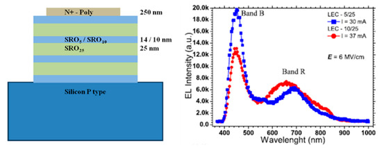
Figure 4.
Schematic (left) and EL spectra (right) of multilayered structure made of nanolayers of R0 =25 and R0 = 10. R0 = 10 or 5 improves the conduction properties, and R0 = 25 is used because of high emission properties [31].
Aside from influencing the light emission spectra, Si contents in SRO also plays a significant role in its conductivity. One approach to improve the electrical characteristics of the LEC while achieving desired emission characteristics is to alternate SRO films with different Si contents. Figure 4 left and right, respectively, show a schematic representation of a multilayer structure and corresponding EL emission spectra. The layered structure uses LPCVD-SRO with R0 = 5 or R0 = 10 as high conductive layers, and R0 = 25 as highly emissive layers. As it can be seen, the multilayered structures have similar emission spectra as those from monolayers, and, due to the presence of higher conduction regions, an improvement in the electrical characteristics is achieved [31].
Another approach to improve electrical injection uses texturized Si substrates. Figure 5 compares maximum achieved EL spectra form LECs based on SRO deposited on polished and textured Si substrates. The textured substrates presented “tips” on the Si surface obtained by reactive ion etching [30]. As can be seen, the spectra present the two characteristic peaks found in single SRO layer LECs, but the structure with textured substrate can achieve emission intensities almost twice as large as compared to the one with polished substrate. Furthermore, electrical power required by the polished substrate for the maximum emission is 2.6 times higher [30].
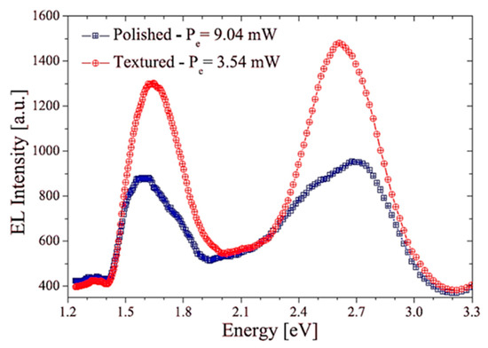
Figure 5.
EL spectra of LECs with polished and textured Si substrate. The two main peaks expected in single layer SRO LECs are clearly identified. However, an improvement of the emission intensity of almost twice is observed in textured substrate, and lower electric power is required [30].
Additional promising results with texturized substrates were also found in devices in which the process was performed by MACE. In this method, metal particles are deposited on the Si surface followed by an etching process in a HF-oxidant based solution [32,33]. The Si beneath the metal particles is oxidized by the solution and then removed due to the presence of HF, leaving a textured surface with an average roughness of 7.5 nm. Figure 6 displays the integrated EL intensity as function of the electric field applied to the LECs both polished and texturized.
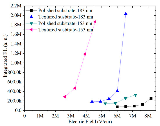
Figure 6.
Integral of EL intensity as function of the applied electric field for devices with polished (solid symbols) and textured (empty symbols) substrates; 183 nm and 153 nm refer to film thickness.
As it can be seen, LECs with substrate texturized by MACE start emitting at significantly lower electric fields, and higher EL intensities are achieved. The explanation for better EL result in texturized substrates is related to the increment of the electric field intensity on the sharper tips, which promotes an increment in the density of electrons available to move through the LEC and stimulate the emission centers along its way. Despite the potentially higher efficiency of these kind of devices, MACE texturization involves processes not currently available in standard CMOS. Then, while this shows there still are ways to improve emitters, it is well worth the effort to optimize the rest of the components (waveguide, photodetectors) to be coupled to the currently well documented CMOS compatible LECs in standard substrates, provided its performance is adequate.
4. SRO\Si3N4 Systems for Emitter-Waveguide Integration
As mentioned, the inclusion of a Si3N4 layer can improve the emission of SRO-based LECs. Its use produces devices with higher electrical stability, as it increases the EL intensity at reduced electric fields [17]. In addition, if the active material is II-SRO, a nitride film can assist in the control of the dose and depth of the implanted Si ions [41]. During this implantation process, an interfacial silicon oxynitride can be formed between oxide and nitride, which has been shown to introduce an additional light emission band in the blue side of the visible spectrum [38]. This can be advantageous for applications, such as chemical and biochemical sensing [4,42,43]. Different Si ion implantation doses in SiO2\Si3N4 systems produce a nitride-oxynitride-SRO stack system with different structural characteristics which, on its turn, can modify the emission spectra of the resulting LECs [38], as observed in Figure 1.
The introduction of Si nitride in the emission enables a significant additional advantage: the possibility of seamlessly embedding the emitter into the waveguide, provided the latter is made of Si3N4. This means there are no coupling issues to be addressed, as the light is directly produced inside the waveguide, presenting spectral characteristics very similar to the PL from the active layer, and Si3N4 is suitable for transmission of such light, as it is transparent for wavelengths (λ) spanning from 0.4 µm to approximately 4 µm, and presents respective refractive index values of 2.1 and 1.9, which represents contrast to SiO2 between 28% and 38%, allowing for reported waveguide losses between 0.001 dB/cm and 0.5 dB/cm [44]. It can also be fabricated using the same standard Chemical Vapor Deposition techniques used for the LECs, and it is very easy to combine with standard SiO2 for core-cladding structures.
The first report of the seamlessly embedded SRO\Si3N4 light emitter approach was published in Reference [25], in which a standard p-n diode was used as the light detector. A scheme of the system is presented in Figure 7.

Figure 7.
Schematic of a monolithic transceiver with light emitting diode based on SRO (LEC), waveguide, and photodiode.
The work proposed a CMOS compatible fabrication process integrating an LEC consisting of a bottom II-SRO layer and a top Si3N4 film which extended to form a slab waveguide. The bottom cladding was buried SiO2 between photoemitter and photodetector. The thickness of this was designed to prevent the light emitted by the SRO\Si3N4 from transferring to the much higher refractive index Si substrate. Figure 8a shows simulations obtained using the software LUMERICAL for light with a wavelength of λ = 509 nm being transmitted by a 60 nm-thick nitride core waveguide (WG). This is one of the main emission peaks by II-SRO, as can be observed in Figure 1a. The cross section of the WG core (gray lines) is centered at z = 0. There is no evanescent field at z = −1.5 µm, assuring no leak of light to the substrate.
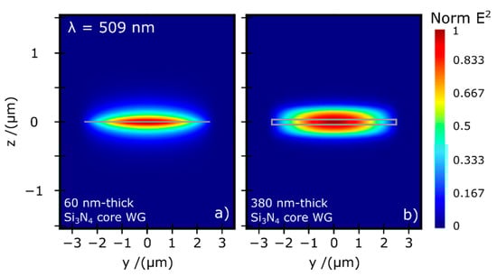
Figure 8.
TE0 mode distributions for waveguides with core of (a) 60 nm-thick and (b) 380 nm-thick Si3N4. The light has a wavelength λ = 509 nm.
This apparently straightforward approach comes with several considerations during the design of the geometries and fabrication processes affecting the size, density, and distribution of the Si nps, as a multitude of factors will influence the behavior of the coupled system. For instance, some of the geometrical parameters of the waveguides are constrained by limits imposed by the emitter, such as the thickness, which has a significant impact in the voltage necessary to drive the emitter. In this regard, there are proposals to decouple this design parameter from emitter and WG, while keeping the nitride seamlessly integrating both devices [45]. This allows for better mode confinements, and consequently thinner cladding layers between core and substrate. Figure 8b shows the simulations for the transmission of the same 509 nm peak but considering a waveguide with core thickness of 380 nm. A clearly larger proportion of the field is transmitted through the core as compared to those with 60 nm-thick cores. However, the core thickness increment is severely limited by tensile stress suffered by Si3N4 when deposited on Si, limiting its thickness to 700 nm in extreme cases [4,44,46].
In addition, the nature of the emitted light must be well considered in the design of the photonic elements. As mentioned, the emitter based on Si-nps has the great advantage of integrability and CMOS compatibility, but a wide emission spectrum is currently unavoidable, and there is no evidence of specific polarization and coherence of the light. This limits the variety of photonic elements that can be implemented. For instance, interferometers are not straightforward to implement.
However, depending on the application, the photonic elements used to transmit and manipulate the light can be carefully designed to use the specific features of the emitted light as an advantage, e.g., there is great potential for wavelength demultiplexing modulation, or for biophotonic sensing applications, in which the visible spectrum can be of great use [42,43,47].
In this regard, taking the well-known SRO-based LEC as a central element, it is necessary to have a study of the photonic components available and the characteristics they must have to move forward towards complex applications for SRO\Si3N4 platform.
5. Photonic Elements
The differentiating factor of the technology here presented as compared to other well stablished Si-photonics platforms is the seamlessly integrated SRO-based light emitter. Then, the elements of a Photonic Integrated Circuit must be designed considering its characteristics and requirements.
Straight WG, bends, and couplers and junctions are examples of basic blocks for more complex photonic circuits [48,49,50].
It is necessary to assure the viability of integrating Silicon nanoparticle-based materials on more complex systems, considering constrains imposed by the SRO/Nitride technology which are different from the C-band currently preferred for communications [44,50]. The material thickness and refractive indexes as those used for the transceiver presented in Figure 7 and reported in Reference [25] can be also used to design more complex elements if the transmission of visible wavelengths in which the LECs emit is assured. Characteristics of the mode transmission and losses can be predicted for different parameters and geometries using diverse theories and tools, including very accurate modern numerical methods and simulation software. This allows to improve the design of the photonic elements in order to assure its adequacy for the specificities of the technology prior to fabrication [48,51].
Figure 9 shows examples of the electric field intensity of the TE0 mode of light with λ = 509 nm as it propagates through a bent waveguide (BWG), a tapper and a Y-splitter; and for λ = 633 nm in a directional coupler. These are some of the basic photonic structures used for more complex PICs, and all simulations considered a 60 nm-thick Si3N4 core and 1.5 µm-thick SiO2 cladding, same as the transceiver reported in Reference [25].
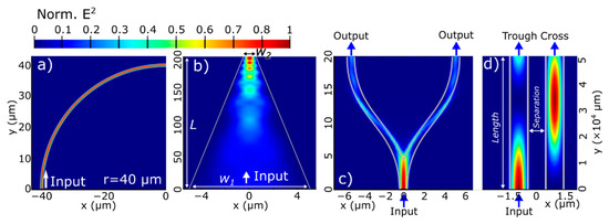
Figure 9.
Simulations of electric field distribution at the middle of a 60 nm-thick Si3N4 core with SiO2 cladding for (a) a bend with radius of 40 µm; (b) a tapper to couple a WG with width w1 = 10 µm to one with w2 = 1 µm; (c) Y-splitter, (d) Directional coupler. All the results are from FDTD calculations for λ = 509 nm in (a–c), and for λ = 633 nm in (d).
Straight WG exhibit an excellent behavior for most applications, with a mean loss of −0.0003 dB/cm, which is equivalent to ~99.99% of transmission in a 1-cm long WG. However, to keep such low losses, some structures required an important amount of chip area as compared to standard electrical circuits or standard SOI technology (non-seamlessly integrable to photo emitters or detectors). For instance, BWGs (Figure 9a) with a bend radius r = 5 μm (typically used in SOI technology [48]) presented significant losses. In fact, transmittance values were found to be below 65% for radii lower than 10 μm. On the other hand, a 20 μm radius showed that wavelengths below 580 nm present transmission above 95%, while longer wavelengths can be considered poorly transmitted for most applications. Nevertheless, for r = 40 μm, negligible loss across the full LEC emission were observed. Tappers (Figure 9b) used to couple light between waveguides with different widths are also area consuming, since its performance is highly dependent on the of coupling length L. In the case of the proposed technology here, L = 200 μm presented transmission values T > 0.98, indicating low radiation losses or null conversion to higher modes [52]. Regarding Y splitters (Figure 9c), it was found that the power at each output port is around 30% of the total input power, when an ideal of 50% is expected. This is caused by losses due to an unoptimized junction. Techniques, such as parametric optimization or particle swarm optimization [53], can be used to improve this, albeit technological limits, such as the resolution allowed by the lithography or patter transfer methods, must be considered. Directional couplers can be an alternative signal splitter (Figure 9d). In these, the mode being transmitted by a WG can be (partially) transferred to an adjacent one. The amount of transferred power depends on the coupling ratio for a given wavelength, which is dominated by two design parameters: the separation of the adjacent WGs (lower separation, larger mode transfer) and their length (the longest the coupler, the larger the power transfer). For shorter wavelengths, the separation of the WG needs to be smaller, representing a difficulty for visible light as compared to IR, since potentially higher lithographic resolution would be required. The simulations showed that for λ = 633 nm, maximum power transfer is achieved around 3.5 mm for a separation of 1 µm, which can be considered demanding in terms of chip area as compared to the other structures here presented. However, this depends on the desired application, and shorter separations will result in smaller areas.
6. Integrated Photodetectors
Important works on the Silicon Photonics portfolio, such as the one by Rahim et al. [44], state that an integrated photodetector is currently not available for silicon nitride platforms. In general, an efficient coupling of the passive photonic elements to photodetectors is also considered one of the major issues for achieving dense optical integration [14], which adds to the issue of light emitter integration previously discussed.
While it has been shown that the use of an emitter based in Si ncs or nps potentially solves the light source problem, the light-guiding silicon nitride restricts the thickness of the passive elements between 60 nm and 400 nm, adding difficulty to the already complicated issue of coupling of external photodetectors, reverting many of the advantages of light source integration. Then, the monolithic integration of the photodetector is also crucial for the viability of the use of nps-based emitting materials. The generation of visible light by these is in this case an advantage, as it means the light is suitable for photon-electron conversion using bulk silicon. The first works reporting a seamless emitter-transmitter-detector demonstrated photosensing using a simple p-n diode embedded in the support substrate [25,34]. The possibility of using the substrate as detecting layer, apart from being an enormous advantage in terms of CMOS compatibility, eliminates the issue of matching propagation constants of guiding nitride and detecting silicon.
However, the thermal treatments needed for the formation of the embedded nanoparticles have a significant influence in the diffusion of the dopants for p-n junctions, and the resulting affectations to responsivity must be carefully considered. The wide spectrum of the proposed LECs is also convenient in this case, as a sufficient large part of the emitted photons can be absorbed by Si at depths coinciding with the depletion region of the junction [25]. Nevertheless, most of the actual emitted light is not transduced, and there is enormous room for efficiency improvements. Figure 10a illustrates an example of the portion of the spectrum which can be absorbed by silicon within the depletion region of an abrupt p-n junction as the one reported in Reference [25].

Figure 10.
(a) PL Spectrum of II-SRO. The shadowed portion of the spectrum is what can be absorbed within the depletion region of a p-n photodiode with the parameters detailed in Reference [25] at Vpn = −35 V; (b) schematics of the process of light absorption, e-h pair generation, and separation in the depletion region for a p-n diode with the fabrication parameters as detailed in Reference [25].
In this case, around 23% of the area of the full spectrum will be absorbed within the depletion region of the junction, which is where most of the signal can be converted from photons to photocurrent, as the rest of the photons will generate electron-hole pairs outside of the depletion region, therefore not being separated by an electric field and eventually recombining without contributing to photocurrent. In addition, non-ideal quantum efficiency and other phenomena further reduce the overall efficiency for converting photons into detected electrons. Nevertheless, the combination of integrated sources, visible light, and the use of standard Si-wafers gives a unique opportunity to think outside the box and propose novel approaches to light sensing architectures. In Reference [22], Alarcón et al. suggest concepts taking advantage of conducting the light wherever needed (e.g., directly into the depletion region of a photodiode) and the use of architectures traditionally used only for electronics, such as a photodetector inspired in a bipolar transistor working in an “backwards” configuration, similar to the Integrated Injection Logic (I2L) [54], but updated and applied to light detection [22].
One promising new approach is the use of silicon nitride simultaneously as optical and electrical material. This is implemented in the Waveguided-sensor (WS) illustrated in Figure 11.
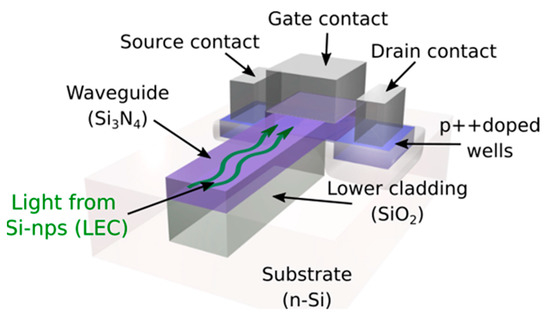
Figure 11.
Concept of a transistor-like photodetector in which the Si3N4 waveguide simultaneously acts as dielectric material in a metal-insulator-semiconductor configuration.
In this concept, light from an integrated LEC based in Si-nps is inserted into the waveguide as in the transceptor reported in Reference [25] and illustrated in Figure 7, but, instead of having a regular photodiode at the end, the nitride waveguide acts as the dielectric material in a metal-insulator-semiconductor configuration, in which source and drain regions are also fabricated to generate a transistor-like device. The light is directly guided to the “channel region”, where relatively small changes in light power can produce larger changes in gate-source electric current flows, effectively achieving electrophotonic amplification.
This means that current flowing through drain due to photogeneration (i.e., dark current subtracted) IDopt is larger than what would be possible to obtain by an ideal photodiode with quantum efficiency η = 1. In an adequate operation point, an electro-optical gain βopt = IDopt/Iph is obtained, where Iph is the number of photons per second multiplied by the charge of the electron.
Figure 12 shows simulation results of βopt for a WS with a channel length of 10 µm considering the detection of light with λ = 600 nm coming from an LEC based on Si-nps.
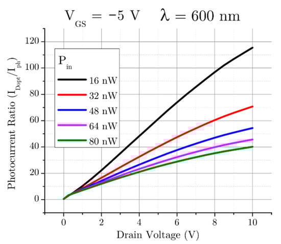
Figure 12.
Results of simulation for photocurrent gain in the integrated photodetector proposed in Figure 11.
The simulations of the fabrication process and the resulting device electro-optical behavior show a gain which increases with drain voltage and decreases with optical power is obtained. The full study on this concept is close to publication, but results from simulations confirm that, just as in emitters and photonic elements, there is a fertile field for new possibilities and ingenious architectures for light detection to be developed, thanks to a whole new concept enabled by the possibility of integrating Si-based light sources, ultimately enabled by the synthesis of nanocrystals and nanoparticles in SiO2.
7. Discussion
CMOS-compatible materials containing light-emitting silicon nanocrystals or nanoparticles can be obtained by various techniques in which it is possible to tune the emission and conduction parameters. The emitted wavelengths are in the visible range, which is suitable for photodetection by standard bulk Si devices, and transmission by nitride-based light guiding architectures.
The integration of emitters, waveguides and photodetectors built around these materials containing Si nanoparticles has been demonstrated in a monolithic emitter-waveguide-photodiode proof of concept, and new processes and techniques for nitride deposition aim to great improvements confinement of light if required.
Simulations considering the emitted wavelengths, available nitride thicknesses, showed the viability of elemental photonic structures like straight and bent waveguides or tapers, even for very conservative lithographic resolutions. More complicated blocks, such as junctions or directional couplers, were also shown to be viable within this strict technology constrains.
The photonic structures must be optimized for the wavelength of interest λ, which will depend on the specific applications. This can be regarded as an opportunity, since it is a route to filter sections of the broad spectrum emitted by the LECs, avoiding the need for external or more complex filters, and using a single light emitter design for all applications within the visible range. This is particularly useful for sensing and biosensing applications, which in addition, are very well suited for the relatively large areas required by the photonic structures. The pattern transfer resolution significantly influences the required chip area for specific photonic structures. Improved freedom on design can be achieved using novel nitride deposition and high-resolution pattern-transferring techniques. Combining this with the broad luminescence spectra provided by the embedded nps, a wide variety of potential applications with optimized designs can be implemented. Nevertheless, even using relatively low resolutions, the structure features are still within the tenths of microns, which is very well suited for high relevance applications, such as Lab-on-a-chip or other sensing systems.
The proposed platform also showed to tackle the issue of integrated self-coupled photodetectors, offering a variety of innovative architectures enabled by the self-contained seamless integration of all the elements necessary for integrated electrophotonics, taking advantage of the visible range of wavelengths emitted by embedded silicon nanoparticles, as it is suitable for light detection by the bulk silicon used in standard CMOS wafers. A device in which the nitride for the photonic structures is also used as a dielectric in a photodetector is described, showing it presents electro-optic gain for the detection of light with radiant powers in the order of nanowatts, reducing the light emission power requirements for the active materials in integrated emitters. The use of CMOS compatible processes and materials improve the possibilities of monolithically integration of all the elements required for active Photonic Integrated Circuits.
8. Conclusions
It has been stablished that a fully monolithic, CMOS compatible, Si-based electrophotonic platform based on SRO/Si3N4 light emitters directly embedded into Si3N4 photonic elements is viable. The currently available optical nitride fabrication technology is suitable for the transmission and manipulation of light in a variety of passive photonic elements in the emission range of the nanoparticle-containing material here presented. Already demonstrated monolithically integrated photodetectors, as well as new photo detecting architectures enabled by the monolithic nature of the concept, along with the possibility of integrating electronic circuitry, allow for the exciting development of fully monolithic electrophotonic systems in standard Si-wafers and standard Integrated Circuits fabrication facilities, with potential use in fields ranging from data transfer to laboratory on chip.
Author Contributions
Conceptualization, A.A.G.-F., M.A.-M.; investigation, A.A.G.-F.; writing—original draft preparation, A.A.G.-F.; writing—review and editing, A.A.G.-F., M.A.-M., and C.D.; supervision, A.A.G.-F., M.A.-M., and C.D.; A.A.G.-F., M.A.-M., and C.D.; experiments and analysis of MACE results, O.P.-D.; simulations and analysis of wavedmos physics, J.H.-B.; funding acquisition, A.A.G.-F., M.A.-M., and C.D. All authors have read and agreed to the published version of the manuscript.
Funding
The project on which these results are based has received funding from the European Union’s Horizon 2020 research and innovation programme under Marie Skłodowska-Curie grant agreement No. 801342 (Tecniospring INDUSTRY) and the Government of Catalonia’s Agency for Business Competitiveness (ACCIÓ).
Data Availability Statement
The data presented in this study are available on request from the corresponding author. The data are not publicly available due to a current lack of a publicly accessible repository.
Acknowledgments
The authors acknowledge the support by CONACyT.
Conflicts of Interest
The authors declare no conflict of interest.
References
- Thomson, D.; Zilkie, A.; Bowers, J.; Komljenovic, T.; Reed, G.T.; Vivien, L.; Marris-Morini, D.; Cassan, E.; Virot, L.; Fédéli, J.-M.; et al. Roadmap on silicon photonics. J. Opt. 2016, 18, 073003. [Google Scholar] [CrossRef]
- Baets, R.G.F.; Subramanian, A.Z.; Clemmen, S.; Kuyken, B.; Bienstman, P.; Le Thomas, N.; Roelkens, G.; Van Thourhout, D.; Helin, P.; Severi, S. Silicon Photonics: Silicon nitride versus silicon-on-insulator. In Proceedings of the Optical Fiber Communication Conference, Anaheim, CA, USA, 20–24 March 2016. [Google Scholar]
- Chiles, J.; Fathpour, S. Silicon photonics beyond silicon-on-insulator. J. Opt. 2017, 19, 053001. [Google Scholar] [CrossRef]
- Blumenthal, D.J.; Heideman, R.G.; Geuzebroek, D.; Leinse, A.; Roeloffzen, C. Silicon Nitride in Silicon Photonics. Proc. IEEE 2018, 106, 2209–2231. [Google Scholar] [CrossRef]
- Sun, C.; Wade, M.T.; Lee, Y.; Orcutt, J.S.; Alloatti, L.; Georgas, M.S.; Waterman, A.S.; Shainline, J.M.; Avizienis, R.R.; Lin, S.; et al. Single-chip microprocessor that communicates directly using light. Nat. Cell Biol. 2015, 528, 534–538. [Google Scholar] [CrossRef] [PubMed]
- Michel, J.; Camacho-Aguilera, R.E.; Cai, Y.; Patel, N.; Bessette, J.T.; Romagnoli, M.; Dutt, B.R.; Kimerling, L.C. An Electrically Pumped Ge-on-Si Laser. In Proceedings of the Optical Fiber Communication Conference; OSA: Washington, DC, USA, 2012; Volume 20, p. PDP5A.6. [Google Scholar]
- Bennett, A.; Chelly, A.; Karsenty, A.; Gadasi, I.; Priel, Z.; Mandelbaum, Y.; Lu, T.; Shlimak, I.; Zalevsky, Z. Fast optoelectronic responsivity of metal-oxide-semiconductor nanostructures. J. Nanophotonics 2016, 10, 36001. [Google Scholar] [CrossRef]
- Brestel, H.; Zalevsky, Z.; Karsenty, A. Enhanced Optical Tunable Excited Capacitor (EOTEC) for Faster Responsivity. In 2018 IEEE International Conference on the Science of Electrical Engineering in Israel (ICSEE); IEEE: New York, NY, USA, 2018; pp. 1–4. [Google Scholar] [CrossRef]
- Wang, X.X.; Zhang, J.G.; Ding, L.; Cheng, B.W.; Ge, W.K.; Yu, J.Z.; Wang, Q.M. Origin and evolution of photoluminescence from Si nanocrystals embedded in aSiO2matrix. Phys. Rev. B 2005, 72, 195313. [Google Scholar] [CrossRef]
- Berman, D.; Aceves, M.; Gallegos, A.; Morales, A.; Berriel, L.R.; Carrillo, J.; Flores, F.; Falcony, C.; Domínguez, C.; Llobera, A.; et al. Silicon excess and thermal annealing effects on the photoluminescence of SiO2 and silicon rich oxide super enriched with siliscon implantation. Phys. Status Solidi 2004, 1, S83–S87. [Google Scholar] [CrossRef]
- Aceves-Mijares, M.; Espinosa-Torres, N.D.; Flores-Gracia, F.; González-Fernández, A.A.; López-Estopier, R.; Román-López, S.; Pedraza, G.; Dominguez, C.; Morales, A.; Falcony, C. Composition and emission characterization and computational simulation of silicon rich oxide films obtained by LPCVD. Surf. Interface Anal. 2013, 46, 216–223. [Google Scholar] [CrossRef]
- Perálvarez, M.; López, M.; Garrido, B.; Morante, J.; Barreto, J.; Cadarso, V.; Riera, M.; Zinoviev, K.; Dominguez, C. Precipitation of highly luminescent phases from PECVD Si suboxides. MRS Proc. 2004, 832, 153. [Google Scholar] [CrossRef]
- Canham, L.T. Silicon quantum wire array fabrication by electrochemical and chemical dissolution of wafers. Appl. Phys. Lett. 1990, 57, 1046–1048. [Google Scholar] [CrossRef]
- Lockwood, D.J.; Pavesi, L. (Eds.) Silicon Photonics II; Topics in Applied Physics; Springer: Berlin/Heidelberg, Germany, 2004; Volume 119, ISBN 978-3-642-10505-0. [Google Scholar]
- Bendayan, M.; Chelly, A.R.; Karsenty, A. Quantum physics applied to modern optical metal oxide semiconductor transistor. Opt. Eng. 2019, 58, 097106. [Google Scholar] [CrossRef]
- Alarcón-Salazar, J.; Palacios-Huerta, L.; González-Fernández, A.A.; Morales-Sánchez, A.; Aceves-Mijares, M. Monolithically Integrable Si-Compatible Light Sources. In Recent Development in Optoelectronic Devices; IntechOpen: London, UK, 2018. [Google Scholar]
- Wang, M.; Anopchenko, A.; Marconi, A.; Moser, E.; Prezioso, S.; Pavesi, L.; Pucker, G.; Bellutti, P.; Vanzetti, L. Light emitting devices based on nanocrystalline-silicon multilayer structure. Phys. E Low Dimens. Syst. Nanostruct. 2009, 41, 912–915. [Google Scholar] [CrossRef]
- Luna-López, J.A.A. Research of the Structural, Optical and Electrical Characterisitics of SRO for Possible Applications to Devices. Ph.D. Thesis, INAOE, Puebla, Mexico, 2007. [Google Scholar]
- Lin, G.-R.; Lin, C.-J.; Lin, C.-K.; Chou, L.-J.; Chueh, Y.-L. Oxygen defect and Si nanocrystal dependent white-light and near-infrared electroluminescence of Si-implanted and plasma-enhanced chemical-vapor deposition-grown Si-rich SiO2. J. Appl. Phys. 2005, 97, 094306. [Google Scholar] [CrossRef]
- Franzo, G.; Irrera, A.; Moreira, E.C.; Miritello, M.; Iacona, F.; Sanfilippo, D.; Di Stefano, G.; Fallica, P.; Priolo, F. Electroluminescence of silicon nanocrystals in MOS structures. Appl. Phys. A 2002, 74, 1–5. [Google Scholar] [CrossRef]
- González-Fernández, A.A.; Mijares, M.A.; Sánchez, A.M.; Leyva, K.M. Intense whole area electroluminescence from low pressure chemical vapor deposition-silicon-rich oxide based light emitting capacitors. J. Appl. Phys. 2010, 108, 043105. [Google Scholar] [CrossRef]
- Alarcón-Salazar, J.; Vázquez, G.V.; Gonzalez-Fernandez, A.A.; Zaldivar-Huerta, I.E.; Pedraza-Chávez, J.; Aceves-Mijares, M. Waveguide-detector system on silicon for sensor application. Adv. Mater. Lett. 2018, 9, 116–122. [Google Scholar] [CrossRef]
- Wang, M.; Huang, J.; Yuan, Z.; Anopchenko, A.; Li, D.; Yang, D.; Pavesi, L. Light emission properties and mechanism of low-temperature prepared amorphous SiNX films. II. Defect states electroluminescence. J. Appl. Phys. 2008, 104, 083505. [Google Scholar] [CrossRef]
- Gonzalez-Fernandez, A.A.; Juvert, J.; Aceves-Mijares, M.; Llobera, A.; Dominguez, C. Influence by Layer Structure on the Output EL of CMOS Compatible Silicon-Based Light Emitters. IEEE Trans. Electron Devices 2013, 60, 1971–1974. [Google Scholar] [CrossRef]
- González-Fernández, A.A.; Juvert, J.; Aceves-Mijares, M.; Domínguez, C. Monolithic Integration of a Silicon-Based Photonic Transceiver in a CMOS Process. IEEE Photonics J. 2015, 8, 1–13. [Google Scholar] [CrossRef]
- Aceves-Mijares, M.; González-Fernández, A.A.; López-Estopier, R.; Luna-López, A.; Berman-Mendoza, D.; Morales, A.; Falcony, C.; Dominguez, C.; Murphy-Arteaga, R.S. On the Origin of Light Emission in Silicon Rich Oxide Obtained by Low-Pressure Chemical Vapor Deposition. J. Nanomater. 2012, 2012, 1–11. [Google Scholar] [CrossRef]
- Morales, A.; Barreto, J.; Dominguez, C.; Riera, M.; Aceves, M.; Carrillo, J. Comparative study between silicon-rich oxide films obtained by LPCVD and PECVD. Phys. E: Low Dimens. Syst. Nanostruct. 2007, 38, 54–58. [Google Scholar] [CrossRef]
- Alarcón-Salazar, J.; López-Estopier, R.; Quiroga-González, E.; Morales-Sánchez, A.; Pedraza-Chávez, J.; Zaldívar-Huerta, I.E.; Aceves-Mijares, M. Silicon-Rich Oxide Obtained by Low-Pressure Chemical Vapor Deposition to Develop Silicon Light Sources. In Chemical Vapor Deposition—Recent Advances and Applications in Optical, Solar Cells and Solid State Devices; IntechOpen: London, UK, 2016. [Google Scholar]
- González-Fernández, A.A.; Juvert, J.; Aceves-Mijares, M.; Dominguez-Horna, C. On the role of the atomic bond types in light emission from Si nanoparticles. AIP Adv. 2017, 7, 055109. [Google Scholar] [CrossRef]
- Alarcón-Salazar, J.; Vásquez-Agustín, M.; Quiroga-González, E.; Huerta, I.E.Z.; Aceves-Mijares, M. Comparison of light emitting capacitors with textured and polished silicon substrates towards the understanding of the emission mechanisms. J. Lumin. 2018, 203, 646–654. [Google Scholar] [CrossRef]
- Alarcón-Salazar, J.; Zaldívar-Huerta, I.E.; Aceves-Mijares, M. Electrical and electroluminescent characterization of nanometric multilayers of SiOX/SiOY obtained by LPCVD including non-normal emission. J. Appl. Phys. 2016, 119, 215101. [Google Scholar] [CrossRef]
- Bastide, S.; Le Quang, N.; Monna, R.; Lévy-Clément, C. Chemical etching of Si by Ag nanocatalysts in HF-H2O2: Application to multicrystalline Si solar cell texturisation. Phys. Status Solidi 2009, 6, 1536–1540. [Google Scholar] [CrossRef]
- Geyer, N.; Fuhrmann, B.; Leipner, H.S.; Werner, P. Ag-Mediated Charge Transport during Metal-Assisted Chemical Etching of Silicon Nanowires. ACS Appl. Mater. Interfaces 2013, 5, 4302–4308. [Google Scholar] [CrossRef] [PubMed]
- González-Fernández, A.A.; Hernández-Montero, W.W.; Hernández-Betanzos, J.; Domínguez, C.; Aceves-Mijares, M. Refractive index sensing using a Si-based light source embedded in a fully integrated monolithic transceiver. AIP Adv. 2019, 9, 125215. [Google Scholar] [CrossRef]
- González-Fernández, A.A.; Juvert, J.; Morales-Sánchez, A.; Barreto, J.; Aceves-Mijares, M.; Dominguez, C. Comparison of electrical and electro-optical characteristics of light-emitting capacitors based on silicon-rich Si-oxide fabricated by plasma-enhanced chemical vapor deposition and ion implantation. J. Appl. Phys. 2012, 111, 53109. [Google Scholar] [CrossRef]
- Negro, L.D.; Yi, J.H.; Michel, J.; Kimerling, L.C.; Chang, T.-W.F.; Sukhovatkin, V.; Sargent, E.H. Light emission efficiency and dynamics in silicon-rich silicon nitride films. Appl. Phys. Lett. 2006, 88, 233109. [Google Scholar] [CrossRef]
- Aceves-Mijares, M.; Gómez-Ramírez, E.; Díaz-Méndez, A.; Rocha, J.M.; Chávez, J.P.; Alarcón-Salazar, J.; Román-López, S.; Domínguez, C.; Merlos, A.; Formatjé, X.; et al. Conservation of the Optical Properties of SRO after CMOS IC Processing. Procedia Technol. 2014, 17, 587–594. [Google Scholar] [CrossRef]
- González-Fernández, A.A.; Juvert, J.; Aceves-Mijares, M.; Domínguez, C. Luminescence from Si-Implanted SiO2-Si3N4 Nano Bi-Layers for Electrophotonic Integrated Si Light Sources. Sensors 2019, 19, 865. [Google Scholar] [CrossRef]
- Juvert, J.; González–Fernández, A.A.; Llobera, A.; Domínguez, C. The effect of absorption and coherent interference in the photoluminescence and electroluminescence spectra of SRO/SRN MIS capacitors. Opt. Express 2013, 21, 10111–10120. [Google Scholar] [CrossRef] [PubMed]
- López-Estopier, R.; Aceves-Mijares, M.; Falcony, C. Cathodo- and Photo- Luminescence of Silicon Rich Oxide Films Obtained by LPCVD. Cathodoluminescence 2012. [Google Scholar] [CrossRef]
- González-Fernández, A.A.; Juvert, J.; Llobera, A.; Aceves, M.; Jimenez-Jorquera, C.; Dominguez, C. PL in Si-implanted Si3N4-SRO and Si3N4-SiO2 bi-layer structures. In Proceedings of the OPTOEL’13, Alcalá de Henares, Spain, 10–12 July 2013; pp. 187–190. [Google Scholar]
- Muñoz, P.; Micó, G.; Bru, L.A.; Pastor, D.; Pérez, D.; Doménech, J.D.; Fernández, J.; Baños, R.; Gargallo, B.; Alemany, R.; et al. Silicon Nitride Photonic Integration Platforms for Visible, Near-Infrared and Mid-Infrared Applications. Sensors 2017, 17, 2088. [Google Scholar] [CrossRef] [PubMed]
- Porcel, M.A.; Hinojosa, A.; Jans, H.; Stassen, A.; Goyvaerts, J.; Geuzebroek, D.; Geiselmann, M.; Dominguez, C.; Artundo, I. [INVITED] Silicon nitride photonic integration for visible light applications. Opt. Laser Technol. 2019, 112, 299–306. [Google Scholar] [CrossRef]
- Rahim, A.; Ryckeboer, E.; Subramanian, A.Z.; Clemmen, S.; Kuyken, B.; Dhakal, A.; Raza, A.; Hermans, A.; Muneeb, M.; Dhoore, S.; et al. Expanding the Silicon Photonics Portfolio With Silicon Nitride Photonic Integrated Circuits. J. Light. Technol. 2017, 35, 639–649. [Google Scholar] [CrossRef]
- Gonzalez-Fernandez, A.A. Studies and Integration of Silicon-based Light Emitting Systems. Ph.D. Thesis, Universitat de Barcelona, Barcelona, Spain, 5 December 2014. [Google Scholar]
- Luke, K.; Dutt, A.; Poitras, C.B.; Lipson, M. Overcoming Si_3N_4 film stress limitations for high quality factor ring resonators. Opt. Express 2013, 21, 22829–22833. [Google Scholar] [CrossRef]
- Passaro, V.M.N.; De Tullio, C.; Troia, B.; La Notte, M.; Giannoccaro, G.; De Leonardis, F. Recent Advances in Integrated Photonic Sensors. Sensors 2012, 12, 15558–15598. [Google Scholar] [CrossRef] [PubMed]
- Chrostowski, L.; Hochberg, M. Silicon Photonics Design; Cambridge University Press (CUP): Cambridge, UK, 2015. [Google Scholar]
- Reed, G.T.; Knights, A.P. Silicon Photonics: An Introduction; John Wiley & Sons, Ltd.: Chichester, UK, 2004; Volume 24, Suppl. 1, ISBN 9780470014189. [Google Scholar]
- Ye, W.N.; Xiong, Y. Review of silicon photonics: History and recent advances. J. Mod. Opt. 2013, 60, 1299–1320. [Google Scholar] [CrossRef]
- Chen, C.-L. Foundations for Guided-Wave Optics; Wiley: Hoboken, NJ, USA, 2006. [Google Scholar]
- Fu, Y.; Ye, T.; Tang, W.; Chu, T. Efficient adiabatic silicon-on-insulator waveguide taper. Photon. Res. 2014, 2, A41–A44. [Google Scholar] [CrossRef]
- Zhang, Y.; Yang, S.; Lim, A.E.-J.; Lo, G.-Q.; Galland, C.; Baehr-Jones, T.; Hochberg, M. A compact and low loss Y-junction for submicron silicon waveguide. Opt. Express 2013, 21, 1310–1316. [Google Scholar] [CrossRef] [PubMed]
- Aceves, M.; Kendall, L.D. Increase of inverse beta of Si transistors due to low-temperature treatments. Electron. Lett. 1979, 15, 282. [Google Scholar] [CrossRef]
Publisher’s Note: MDPI stays neutral with regard to jurisdictional claims in published maps and institutional affiliations. |
© 2021 by the authors. Licensee MDPI, Basel, Switzerland. This article is an open access article distributed under the terms and conditions of the Creative Commons Attribution (CC BY) license (https://creativecommons.org/licenses/by/4.0/).