Article

Determination of the Exact Orientation of Single-Crystal X-ray Optics from Its Glitch Spectrum and Modeling of Glitches for an Arbitrary Configuration

1
International Science and Research Center “Coherent X-ray Optics for Megascience Facilities”, Immanuel Kant Baltic Federal University, 236022 Kaliningrad, Russia
2
Center for Free-Electron Laser Science, 22607 Hamburg, Germany
3
European Synchrotron Radiation Facility (ESRF), BP 220, 38043 Grenoble, France
*
Author to whom correspondence should be addressed.
Crystals 2021, 11(5), 504; https://doi.org/10.3390/cryst11050504
Submission received: 1 April 2021 / Revised: 23 April 2021 / Accepted: 27 April 2021 / Published: 2 May 2021

Abstract

:
X-ray optics made of single-crystal materials are widely used at most of the X-ray sources due to the outstanding properties. The main drawback of such optics—the diffraction losses, also known as glitches of intensity in the energy spectrum of the transmitted/diffracted beam. To be able to handle this negative effect, one needs a reliable way to simulate the glitch spectrum in any configuration. Here, we demonstrate the way of precisely determining the crystallographic orientation and unit cell parameters of optical elements just from a small glitch spectrum with the consequent possibility of simulating glitches for any energy.

Graphical Abstract

1. Introduction

Single-crystal materials have outstanding properties, such as robustness, good reproducibility, and a small number of defects that lead to low background scattering. That is why those materials are favored for X-ray optics production. Such optical elements as monochromators, focusing mirrors, compound refractive lenses (CRLs) [1], attenuators, windows, beam intensity monitors, etc., are often made of single-crystal silicon, sometimes germanium or diamond. Unfortunately, X-ray optics made of crystalline materials have one significant drawback—diffraction losses due to undesired Bragg/Laue scattering, usually called the “glitch effect” [2]. The effect manifests itself as follows: at some energy of the incident X-rays, the main beam, transmitted through or diffracted from the crystalline optical element, loses a part of its intensity. This happens because the incident beam of the wavelength λ satisfies some undesired Bragg condition:
2d sin θ = n λ,
where n is an integer, and θ is the angle between the incident beam and the family of lattice planes with interplane distance d.
This parasitic diffraction diverts some part of the intensity at an angle 2θ to the incident beam. For the optical elements based on diffraction (monochromator) the glitch effect is observed due to the multiple-beam diffraction, when several sets of crystal planes satisfy Bragg’s law [3,4].
The glitch effect was mostly observed in spectroscopic measurements, when the energy of the beam at a studied sample changed continuously, usually using a monochromator [3,4,5,6,7,8]. During such change, the intensity of the beam drops at some energies—this drop is caused by the “glitch effect”. The easiest way to correct for the drops of the intensity is to measure the intensity before the sample (I0) and normalize the measured signal from the sample by the I0. Unfortunately, this method often still leaves some artifacts in the measured signal [7], so some other methods are needed.
One of the ways to avoid glitches in the optics working in transmission geometry (such as CRLs) is to decrease its crystallinity. For example, one can make a CRL with polycrystalline material; for this purpose, polycrystalline diamond was tested [9,10,11]. However, it will not eliminate the problem completely, because the glitches would still be generated by each small crystallite. Additionally, optics made of polycrystalline material often generate undesired speckles in the transmitted beam. The other way is to use bent crystals—for example, bent monochromators [3]. This method can be more technically demanding, especially in terms of achieving a very precise surface shape, a low surface roughness, and low subsurface damage [12]. If this is not achieved, the uniformity of the beam may decrease [13].
Two more ways to decrease glitches are by tuning a double crystal monochromator [14] or by using a cutoff mirror to suppress some individual glitches [15]. Both methods require additional hardware changes and do not eliminate all glitches. Additionally, for these methods, it would be useful to calculate the exact glitch spectrum for any configuration of the monochromator. Such a calculation can be made using the method proposed in this paper.
Another method against glitches is to align the optical element such that the X-ray beam is parallel to one of its main crystallographic directions [16]. However, this is just minimizing the issue, but not eliminating it. As will be shown at the end of the paper, the number of glitches is reduced in this case, but there are still a few left. Again, the required orientation of the optical element can be easily determined using the algorithm described in this paper.
One more approach for monochromators is to use the change in polarization of the primary beam induced by so-called “multiple-beam dynamical effects”. Such effects can lead to energy transfer between different excited reflections as well as the change in polarization of diffracted beams. It is possible to derive the glitches effects from a two-dimensional (2D) spatial distribution of the primary diffracted beam by measuring the signal using a 2D detector [17,18]. This method is complicated and might not work for arbitrary samples and beamline configuration.
Several beamlines provide a table of the measured “glitches” [19]. It makes sense if there are no changes in the setup of the beamline. Unfortunately, even a small error in the energy induced by an error of the monochromator tuning can lead to rather big changes in the glitches spectrum. The method described in this paper can successfully replace a premeasured table. After any change in the beamline configuration, all possible positions of the glitches in the whole range of working energies of the beamline can be precisely calculated by measuring a small glitch spectrum (a couple of keV) and processing it using the described algorithm.
A practical way to eliminate the glitches that are being used at modern synchrotrons is to measure a spectrum, then rotate the monochromator crystals azimuthally and remeasure the spectrum. The two resulting spectra can be stitched together filling the regions affected by glitches with the corresponding regions from the second spectrum. This method requires twice the time of measurements, and also, some regions of the spectra can still be affected by glitches in both measurements. Additionally, to choose the optimal rotation of the monochromator, one would need to know its current orientation. This task can be easily accomplished using the algorithm described in this paper.
Another way to fight glitches is to smooth the measured spectra with some high-pass filter [20]. This method works fine because the glitches usually produce sharp drops of intensity, so a high-pass filter can eliminate most of the glitches. The problem is that in this way, the actual measured data can also be affected. Alternatively, the regions affected by the glitches can be just excluded from further analysis, but to do so, one has to know exactly at which energies the glitches were observed to avoid discarding real data. The algorithm of glitches prediction described in this paper can help to determine all glitches in the spectrum reliably and unambiguously for further masking or smoothing.
The glitches in monochromators are the most often observed and well-studied compared to glitches in other optical elements. This is due to the fact that monochromators are used at most of the beamlines at all synchrotrons and also at laboratory sources. Due to the natural design of the monochromator, it is usually already diffracting most of the intensity into the direction of its primary reflection. Usually, the main reflection of the monochromator corresponds to a strongly diffracting set of planes, such as (111) or (220) for silicon. Therefore, the other set of planes that can be “excited” will not be strong enough to parasitically diffract most of the beam.
For the crystalline optics working in transmission mode, such as CRLs or attenuators, the situation is much worse. Each strongly diffracting set of planes can be excited by a glitch, and the whole beam can be diverted into the direction of parasitic diffraction. So, the whole beam may be lost. This might happen even without scanning the energy, especially for harder X-rays (>20 keV)—the probability to “catch a glitch” is increasing with the energy of the X-rays. That is why in this paper, we are focusing on the glitches observed in the crystalline optics working in transmission mode.
There were attempts to simulate glitches for some special cases [21]. However, for such a simulation, the exact orientation of the optical element with respect to the beam must be known. Our previous attempt to find the orientation by using a 2D detector to measure Bragg peaks for CRLs has failed due to the low precision of the measurements. So, this method is quite complicated technically and also time-consuming. From the data analysis, we have found that to determine the precise orientation of a CRL, a small angular step (below 0.01 degree) and a large range of angles are required.
The algorithm of glitches simulation described in this paper can be used for any single-crystal optical element with a cubic cell. The presented method requires only a small glitch spectrum measurement at the actual beamline configuration. It allows us to determine the exact orientation of the optical element with respect to the incident beam and its cell parameters. We will also describe a way to efficiently be rid of the glitches in any experiment.

2. Materials and Methods

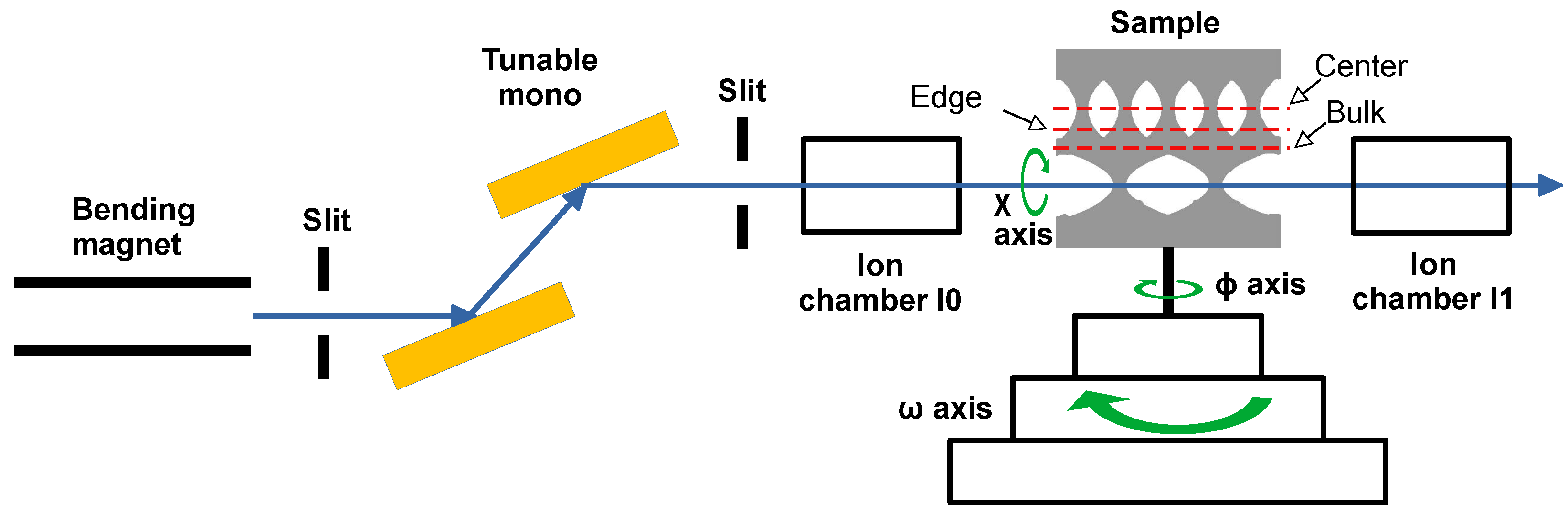
2.1. Experiment Description

The experiments were performed at the Swiss-Norwegian Beamlines (SNBL) BM31. It is a bending magnet source at European Synchrotron Radiation Facility (ESRF), France.
Four different types of diamond samples were measured:
  • No profiling plate, supplied by Element Six Ltd., Santa Clara, CA (USA) [22];
  • One-dimensional CRL, which consists of two sets of compound refractive lenses, machined by Micro Usinage Laser (MUL), Grattentour, (France) [23,24];
  • One-dimensional CRL, which consists of three sets of compound refractive lenses, manufactured in Saint Petersburg, Russia by New Diamond Technology (NDT) [25];
  • Two-dimensional lens, grown at the Technological Institute for Superhard and Novel Carbon Materials (TISNCM), Troitsk, Russia [26].
The samples were made from different diamond materials and had different material qualities in terms of purity, crystallographic orientation, and ideality, which was described in the papers [2,24,25,26]. All samples were measured in so-called EXAFS mode when the energy of the incident beam was constantly changed, and at the same time, the beam intensities of both incident (I0) and transmitted through the sample (I1) beams were measured using ionization chambers (see Figure 1). The step of the scan was limited by the resolution of the monochromator of 1 eV. The sample was mounted at a three-cradle goniometer utilizing 3 axes during the measurements. More experimental details can be found in [27,28].
It is worth noting that the glitches recorded by the I1 chamber are caused by both the monochromator (single-crystal silicon) and the sample. To eliminate the glitches caused by the monochromator as well as to compensate the refills of the synchrotron ring with electrons, the transmitted intensity was normalized by the incident intensity (I1/I0) and then by its smoothed version (to compensate for the change in absorption). Some examples of the normalized glitch spectra for different orientations of the lens MUL are presented in Figure 2.
For the first CRL (MUL) [24], we recorded several scans at different angles χ (rotation around the beam—see Figure 1). The thick part of the lens (bulk) was scanned at χ = 0°, χ = 15° and χ = 30° and the thinner part (edge of the lens) at χ = 0°, χ = 10°, χ = 20°. For most of the samples, the X-ray beam was parallel to the crystallographic direction [10]. Only for the second CRL (NDT), the beam was parallel to the direction [110].

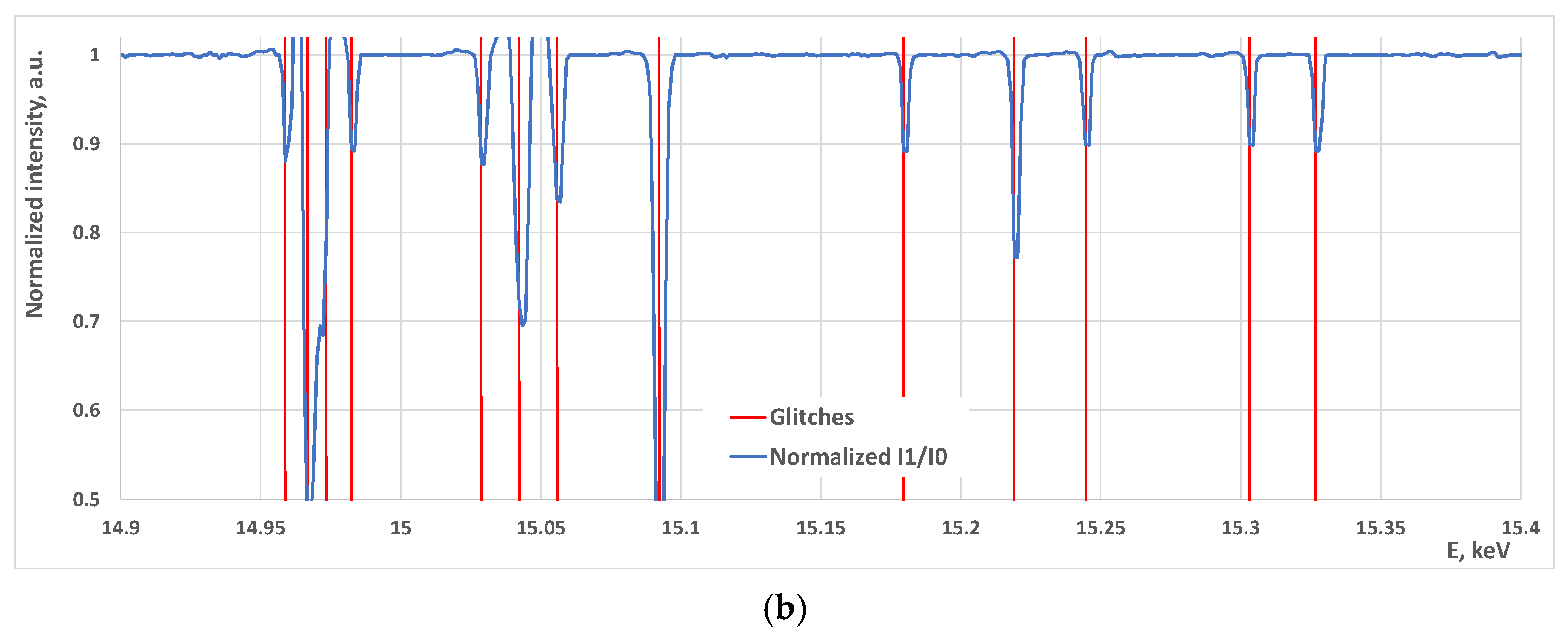
2.2. Extracting Glitches from the Experimental Data

The intensity values I0 and I1 measured by the two ion chambers (Figure 1) are recorded for each energy. Due to the “refill” and glitches in the monochromator, the incident at the sample intensity I0 is changing in time. Therefore, the intensity measured after the sample has to be normalized by the incident intensity (basically dividing I1/I0—see Figure 1). After the normalization, the average intensity grows with energy (red line at Figure 3).
This is due to the fact that the absorption inside the optical element is decreasing with the energy increase. This effect we eliminate in the following way: we smooth the curve (blue line in Figure 3) and divide the original curve by the smoothed one. As a result, we obtain the normalized glitches spectrum (blue line in Figure 4). Then, to find the exact position of the glitches, we smooth the resulting curve a little and take a derivative (green line at Figure 3). At the energies where the derivative is changing sign from “−” to “+” and where the normalized glitch spectrum drops below some threshold, we declare a glitch.
As can be seen from Figure 4, the precision of the glitches determination is not ideal—within several eV, but as will be shown later, this is sufficient for further analysis.
Here is a step-by-step description with computational details of the process to extract glitches:
  • Divide I1/I0 to get normalized spectrum;
  • Make a smoothed version of the curve (running median with 15 pixels window);
  • Divide the normalized curve by the smoothed one;
  • Smooth the resulting curve a little (running median with 3 pixels window);
  • Calculate the derivative of the resulting curve;
  • Select regions with intensities smaller than some threshold (like 0.97) as potential glitches;
  • Analyze derivatives in the preselected regions. If the derivative changes the sign from “−” to “+” and has some reasonable amplitude (usually 1–5), declare this as a glitch.
In order to process all glitch spectra collected from different samples, we have written a program that takes as an input a text file with glitch spectrum, smoothing radius, and the derivative threshold and produces a text file with the energies of the found glitches. This program can be found at GitHub [29].

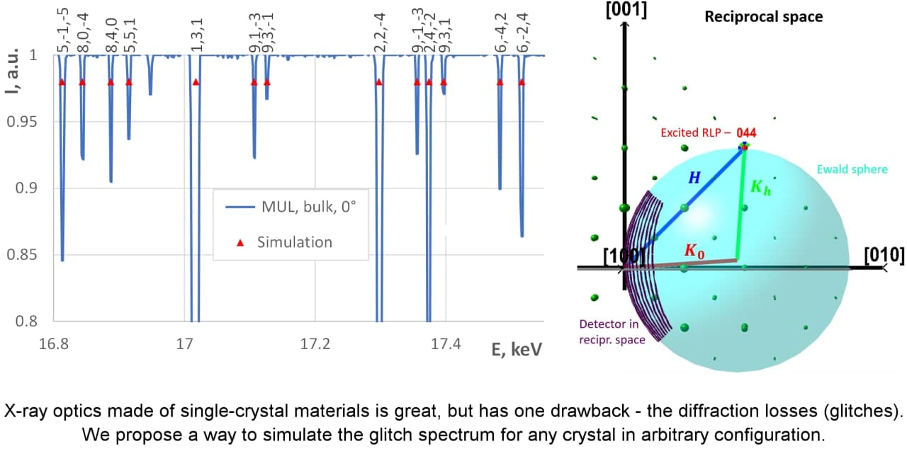
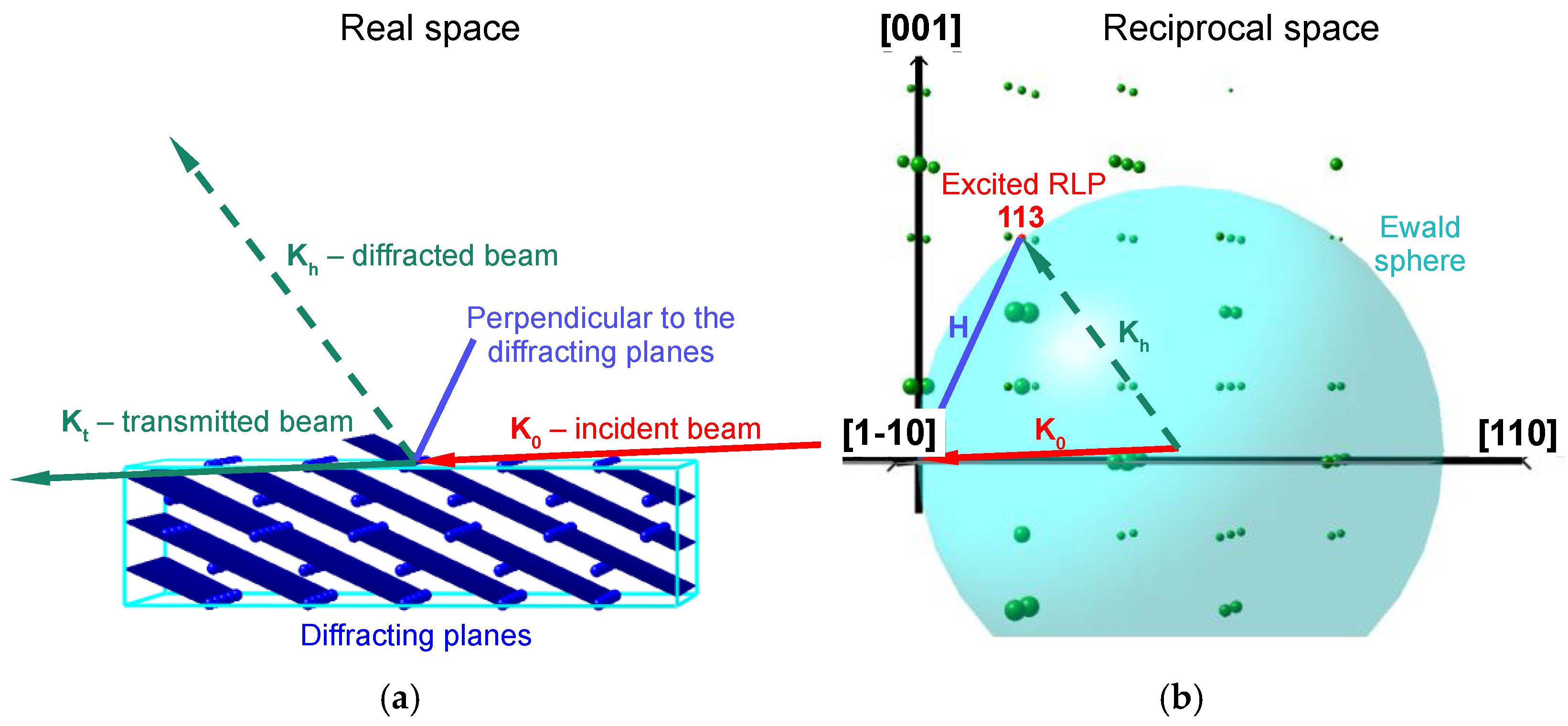
2.3. Explanation of Glitches

A Diffraction occurs when the X-ray beam of certain energy, impinging on a crystal, accidentally satisfies the Bragg condition for a selected set of crystal planes. Therefore, the intensity of the transmitted (or diffracted for monochromator) beam will be reduced. Each set of crystal planes in real space can be described as a reciprocal lattice point (RLP) in reciprocal space. Considering this, the glitch formation is easier to explain in reciprocal space—the undesirable diffraction occurs when some RLP is intersected by the Ewald sphere build for current experimental parameters (incident beam direction and energy). Figure 5 explains the glitches’ formation in both spaces [30].
The radius of the Ewald sphere (K = 1/λ) can be calculated from the energy of incident beam (E) as:
K = E [ k e V ] 12.3984 ,
This means that the change in the energy of the incident X-rays leads to the change in the Ewald sphere radius, and so, the sphere can intersect different RLPs. That explains the appearance of glitches at different energies, when the sphere of corresponding radius K intersects different RLPs. The animated GIFs showing the process of glitches formation were made using the program XViz [31] (see at GitHub [29] in Supplementary Material).

2.4. Extracting Glitches from the Experimental Data

Forward simulation of the glitches (for given unit cell (UC) parameters and incident angles Omega and Phi, or actually wave vector K0) is performed in the following way. All energies in some range with some reasonable step (usually 5 eV) are being checked for a not forbidden reciprocal lattice point (RLP) with a reciprocal vector H lying close (with some tolerance ε, usually ε = 0.08) to the Ewald sphere calculated for current parameters:
( H x K 0 x ) 2 + ( H y K 0 y ) 2 + ( H z K 0 z ) 2 < ε × | K | ,
where Hix,y,z and K0x,y,z are the components of the vectors H and K0.
Only RLPs with vector length | H | 2 × | K | should be probed. If for current energy, a “candidate” RLP with indexes hkl is found, the exact glitch energy E t r u e for this point can be calculated as:
E t r u e = 12.3984 × h 2 + k 2 + l 2 2 × a × sin ( θ ) ,
where a is a cell parameter for the cubic lattice.
At this step, we constrain the solution of the problem to only cubic lattices. Taking into account that most of the X-ray optical elements are made of crystals with cubic lattices, this is a rather justified simplification. However, the whole algorithm can be extended to an arbitrary unit cell, if needed.
The RLP with the found energy is marked as already found, and the search for other RLPs that are close to the Ewald sphere for all scanned energies is carried on. The list of the found RLPs with the corresponding exact energies is called further “predicted glitch spectrum”.

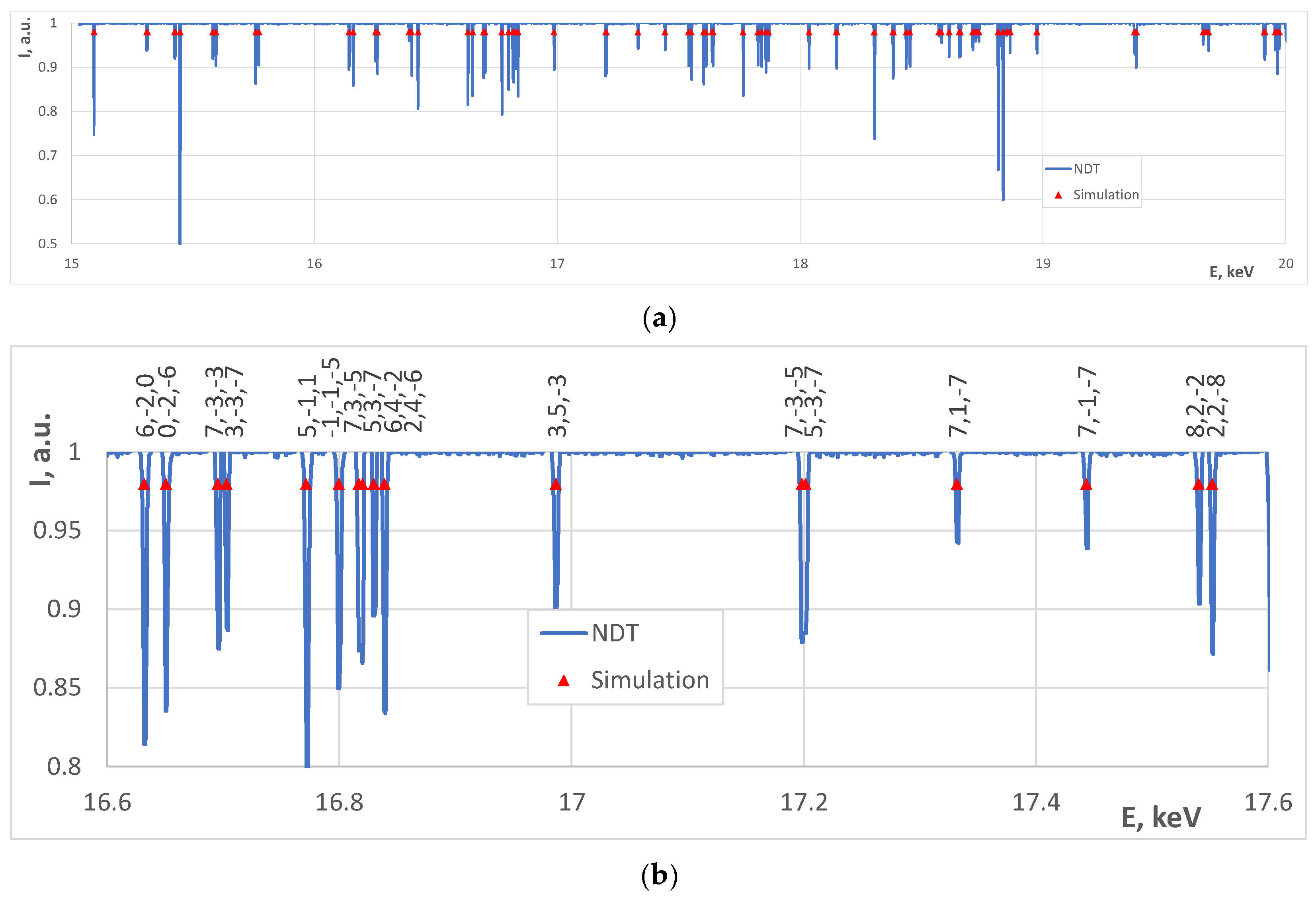
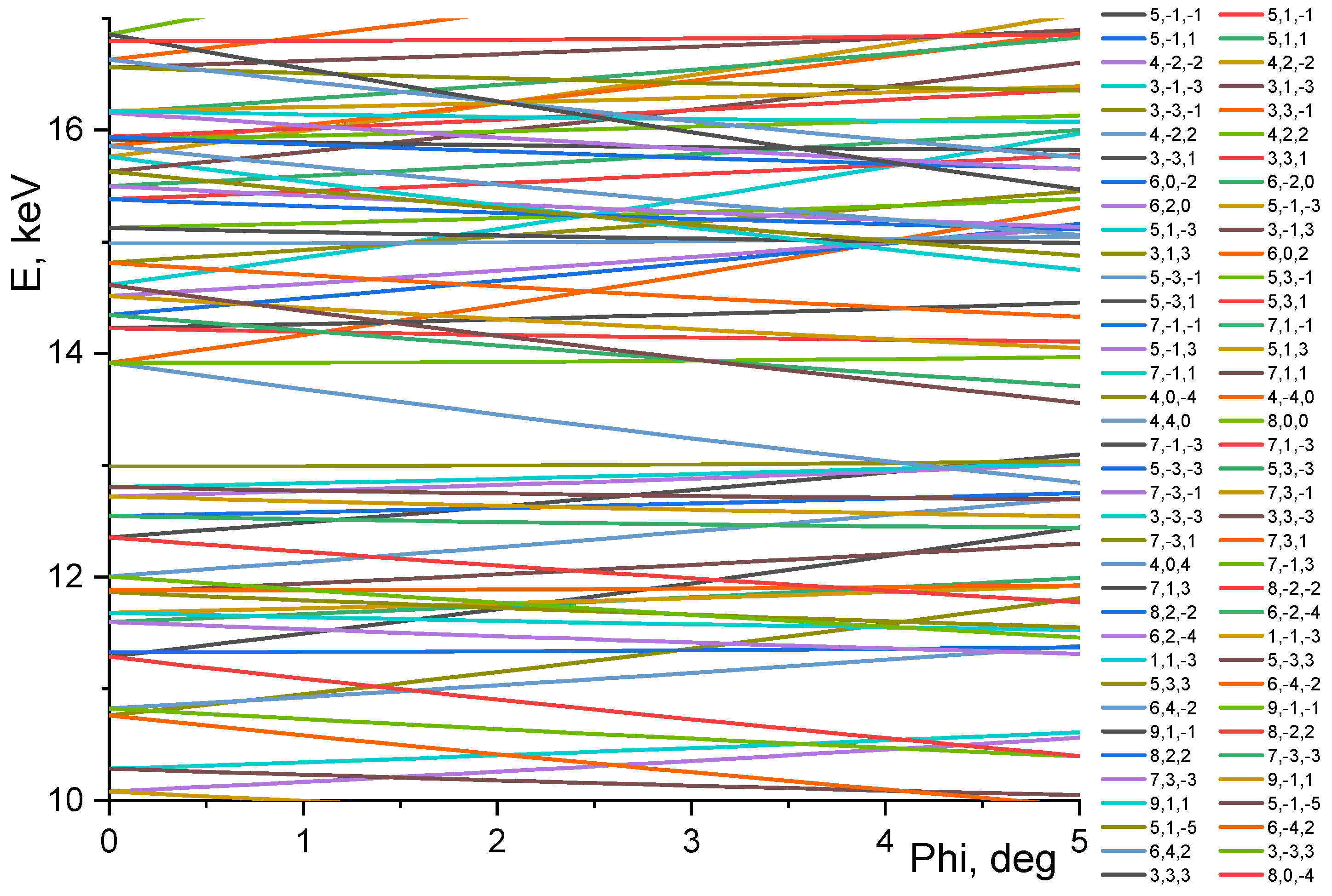
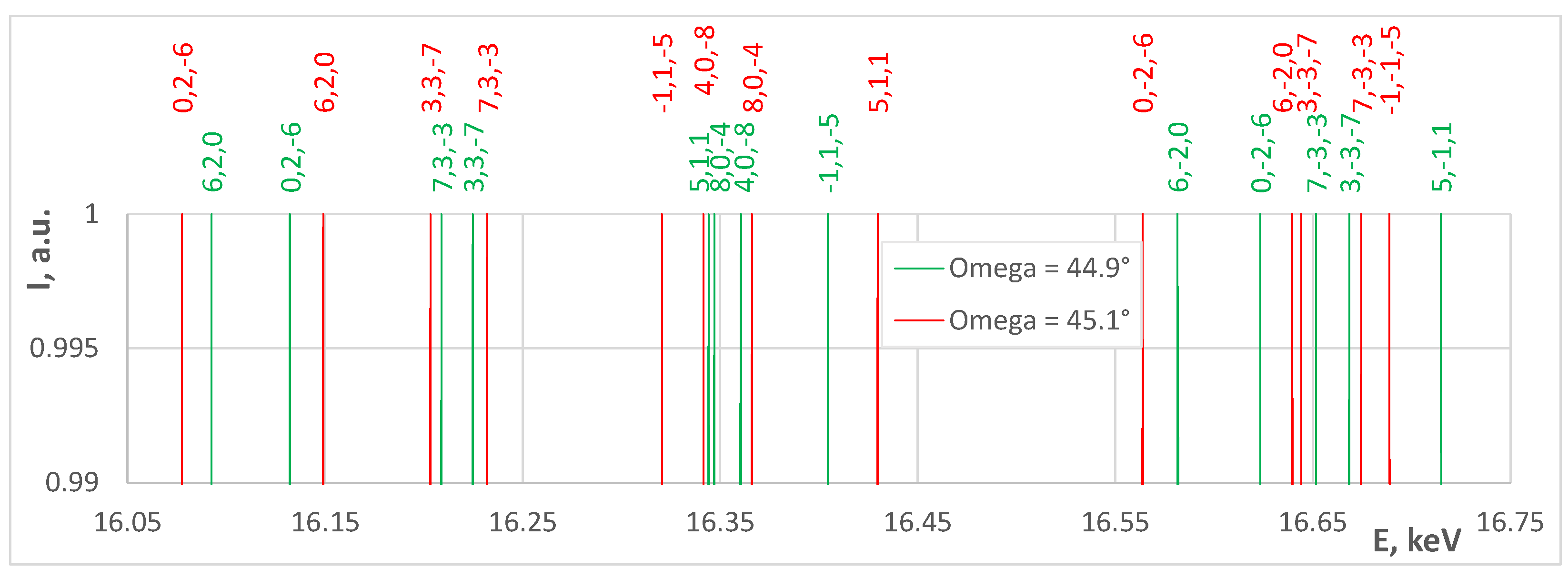
2.5. Finding Approximate Orientation and Indexing Glitches

The obtained list of energies, at which the glitches were observed, is used for finding the orientation of the lens (in fact its crystallographic axes) with respect to the incident beam. First of all, we are searching the space of three parameters (UC, ω, ϕ) to find a minimum of the error between the energies of the measured glitches and predicted in each orientation and for each UC parameter. The error is calculated in the following way: each measured glitch is compared to all predicted glitches, and the minimum squared distance is saved. Then, all such distances for measured glitches are summed (dividing by the number of measured glitches). The square root of the result is considered as the error in the glitches determination. So, the error in fitting is actually the standard deviation of measured and simulated energies of the glitches:
e r r o r = i = 1 N ( E _ e x p i E _ s i m i ) 2 N
where E _ e x p i is the energy of a measured glitch (N measured glitches in total), and E _ s i m i is the energy of the closest simulated glitch.
After finding the best combination of UC, ω, and ϕ, the Miller indexes of the predicted glitches, which are the closest to the measured ones, are attributed to the corresponding measured glitches (we call this process “indexing” similarly to the process of attribution Miller indexes to the Bragg peaks measured during crystallography experiments). The indexed spectra of glitches can be used for the next step of the refinement of the determined parameters.
Here is a step-by-step description of the process of glitches indexing:
(a)
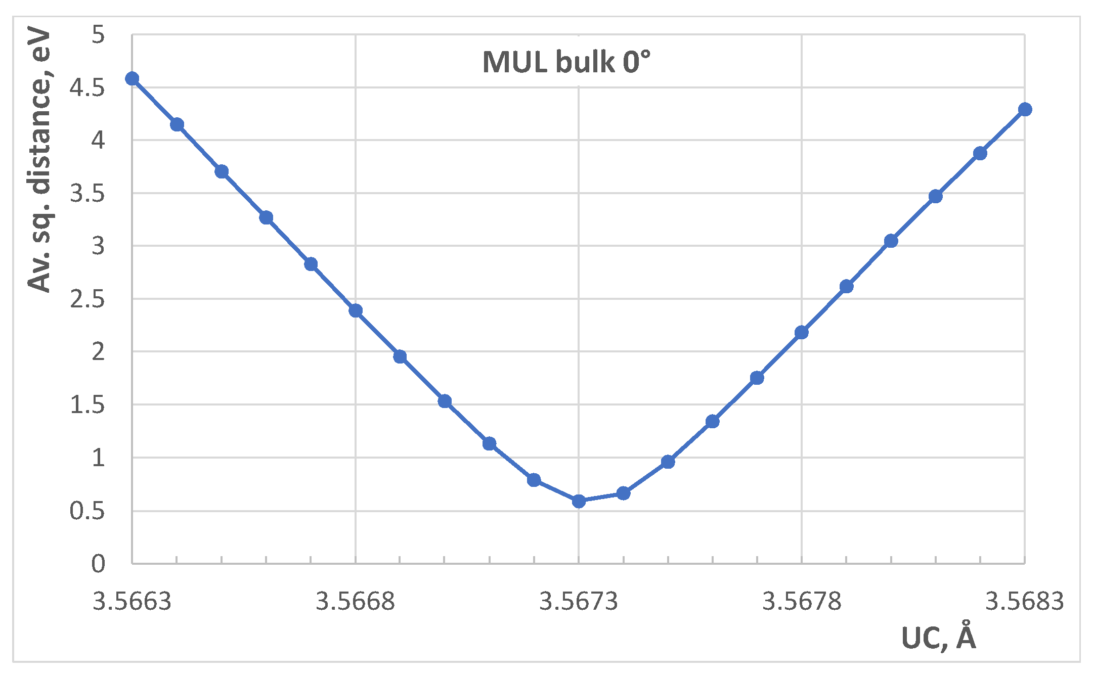
Search of the UC, ω, ϕ (in some range with fixed step size), while minimizing the average square distance between found and predicted glitches;
(b)
Repeating the first step 1–2 times narrowing the windows and minimizing the step of search parameters (UC, ω, ϕ);
(c)
Indexing the measured spectra by assigning to each glitch the Miller indexes of the closest predicted Bragg peak.
The process of analysis of the experimental glitch spectra is computationally heavy due to the fact that the glitches are very sensitive to the orientation and cell parameters of the lattice. In order not to miss the correct orientation, one has to do the search with a rather small step (at least 0.01 Å for UC and 0.5° for the angle). Additionally, the range of orientation can be rather large due to the miscut of the crystal slab and due to an error in setting up the optical element. Luckily, the process of the initial search is highly parallelizable, so it is possible to perform the search in just minutes. For this task, a program in C++ was written [29].

2.6. Determining the Exact Orientation and Cell Parameters
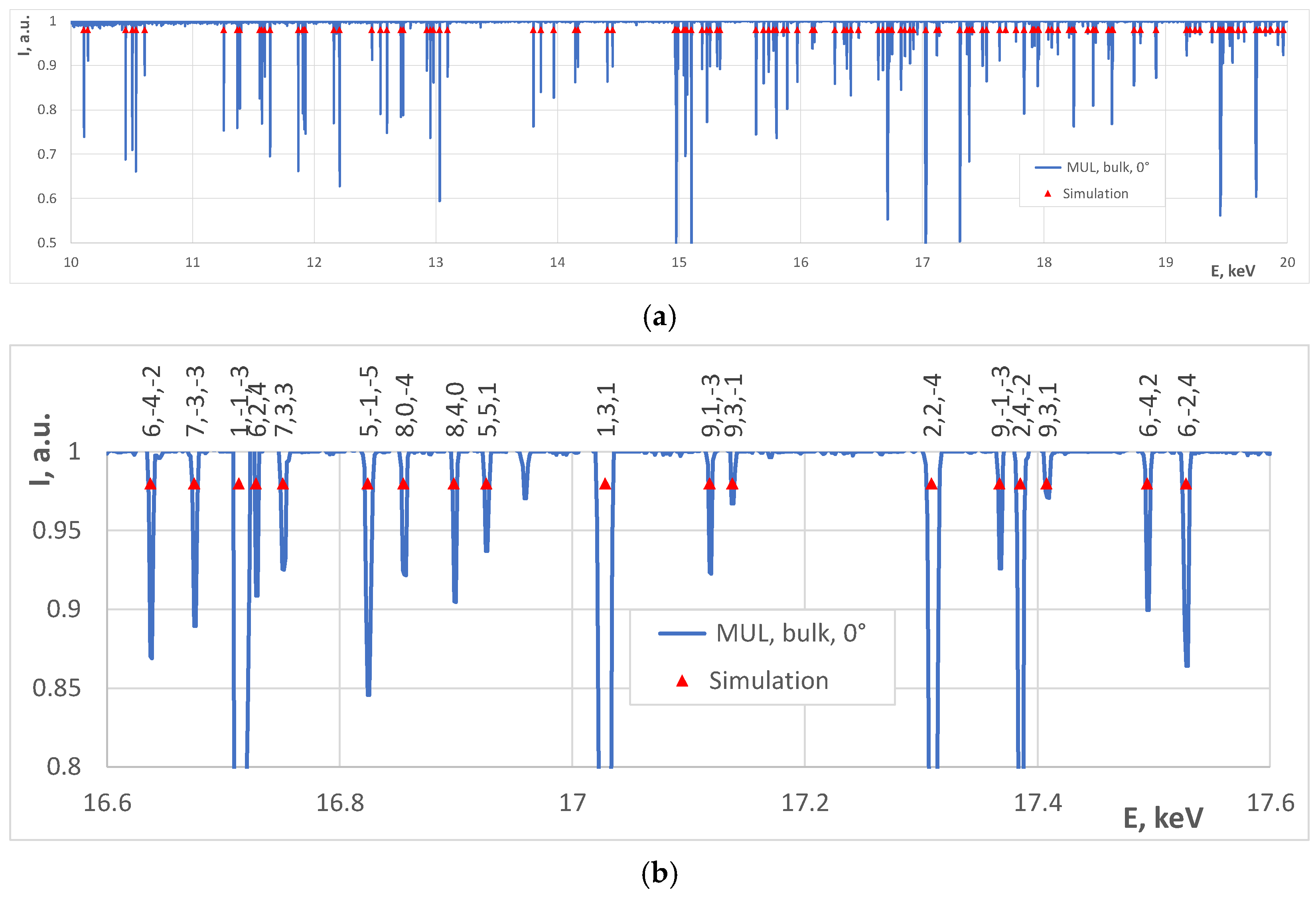
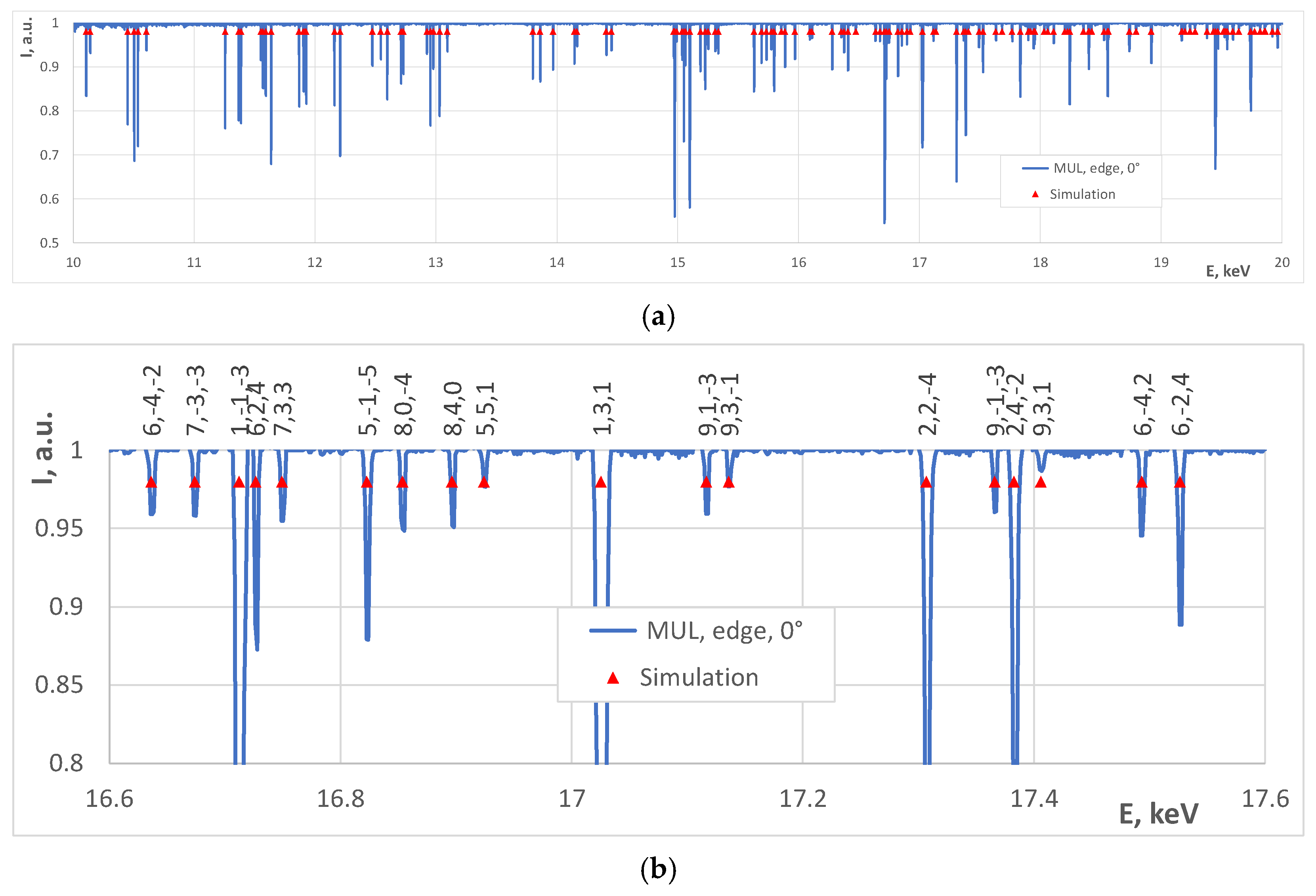
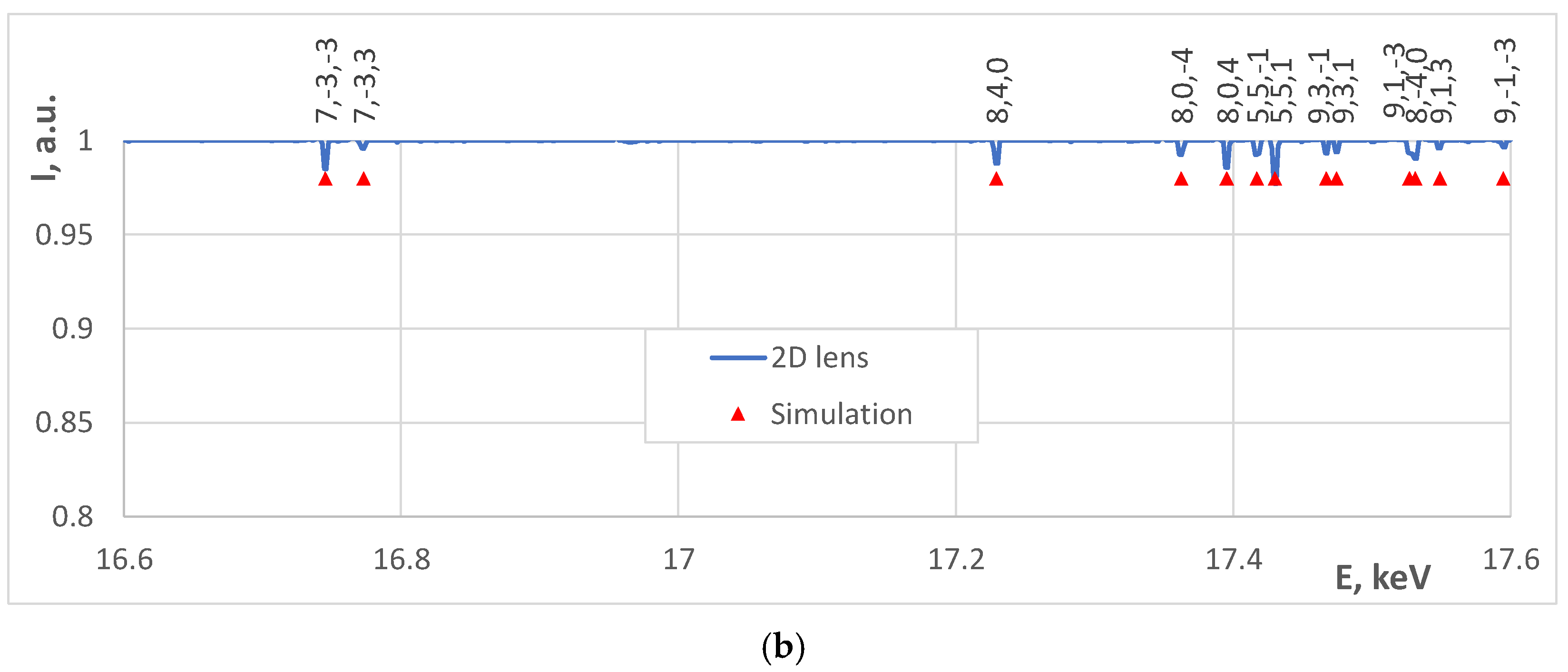
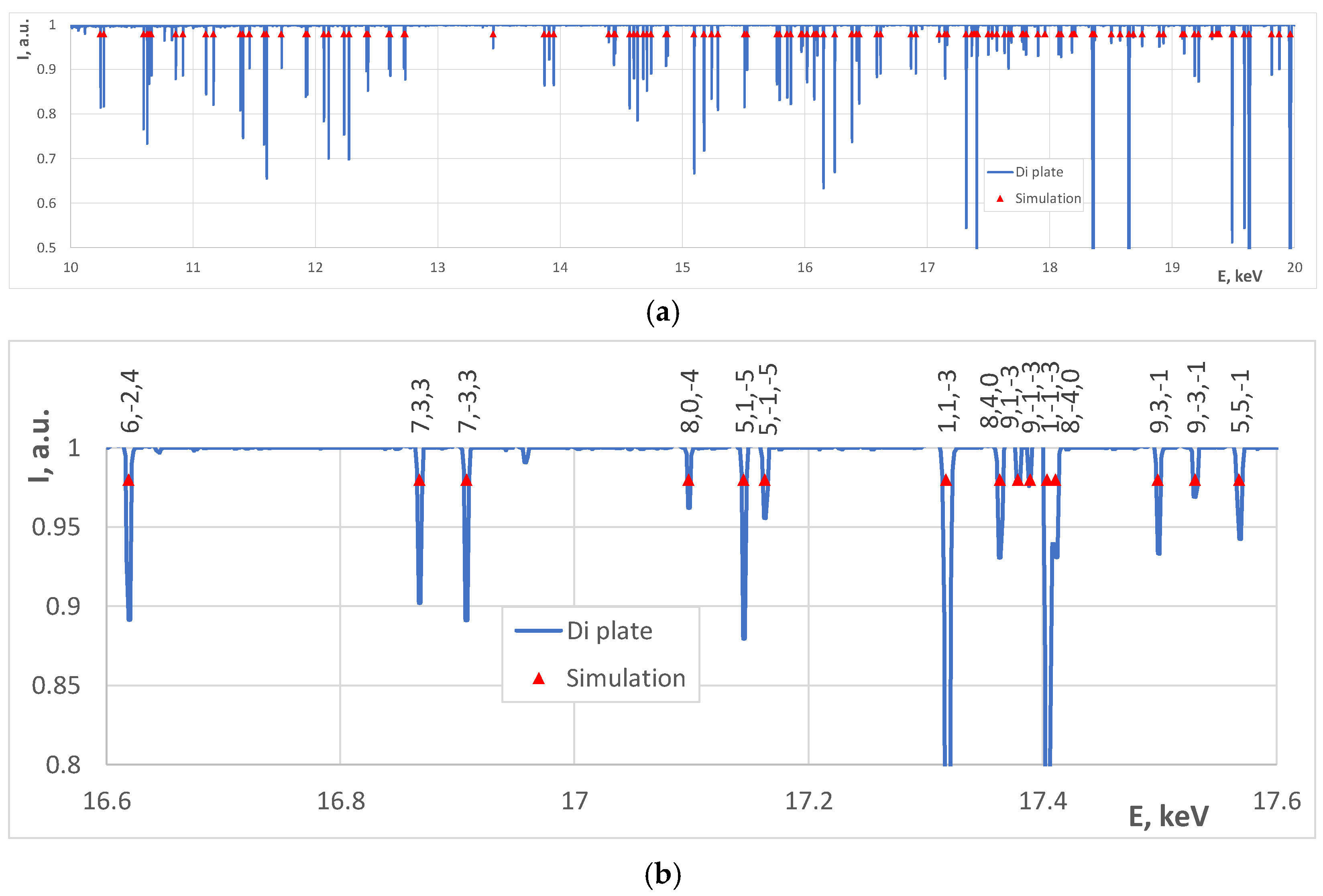
After the determination of the approximate lens orientation, we can refine it using an analytical approach described in [30]. In order to do so, we can use the indexed glitch spectra, described in the previous section, and run the analytical solution that will derive the exact orientation and the UC parameters. As we have demonstrated in [30], it is enough to have just three indexed glitches to get the orientation and the UC parameter (in the case of the cubic cell). However, having more indexed glitches improves the precision of the determination of the parameters. The refinement program is written in Python and is using NumPy function linalg.lstsq to solve an overdetermined system of equations [29].

3. Results

The results of the whole pipeline of processing the experimental glitches spectra are summarized in Table 1. The resulting error is close to 0.5 eV, which is just half of the energy step size, used at the experiment and also better than the precision of the glitch position determination. Such high accuracy can be achieved only if the beamline is properly tuned, and the X-ray energy is well calibrated.
If the surface orientation of the crystal is known, this can speed up the calculations. However, in principle, whole analyses can be done even without any prior knowledge about the optical elements. For example, the NTD lens had {110} surface, while all other samples had {001} surface; as can be seen from the Table 1, this did not create any problem for our method—the ω angle is close to 45° for NDT.
Due to the fact that the precision of the experimental glitches determination is comparable to the resulting error in the fitting of the glitches, it makes no sense to compare the determined and predicted energies of glitches. For quantitative comparison, one should refer to Table 1. Instead, we present some measured normalized spectra together with the predicted glitches positions for all samples. Additionally, a magnified region with the Miller indexes for each glitch is shown to demonstrate how precise the prediction is (Figure 6, Figure 7, Figure 8, Figure 9 and Figure 10).
As can be seen from Figure 6, strong reflections such as 113 or 224 cause strong glitches. This is consistent with the physics of glitches formation, and also, it confirms the correctness of the solution.
The drop of intensity for the edge part of the MUL lens (Figure 7) is much lower than for the bulk part of the same lens (Figure 6). This is due to the fact that the thickness of the material of the lens at the edge part is smaller (see Figure 1). However, this effect is not due to the absorption in diamond, as was mistakenly reported previously [28], but due to diffraction. The fact that the drop of intensity is not too deep suggests that the thickness of the diamond should be still smaller or comparable to the extinction length for the reflections that correspond to the observed glitches. Therefore, only part of the intensity is diffracted away at the glitches’ positions. Additionally, for the central part of the lens, this diffracted part of intensity is smaller.
The 2D lens was much thinner than the MUL lens; therefore, the drops of intensity, as described above, were also much smaller (Figure 8). As can be seen from Figure 8b some glitches overlap, but this is not a problem for our algorithm. The reader can use the program from [29] to get the exact energy for each glitch.
At the magnified spectra of the diamond plate (Figure 9b), one can see a not-predicted glitch at E = 16.95 keV. This glitch is most probably a monochromator glitch that was not fully eliminated during the normalization process. In fact, this glitch is also visible in Figure 6b at the same energy that has to be the case if this glitch originates from the monochromator.
The lens NDT had the surface orientation [110]; therefore, the found orientation was close to the angle ω = 45°. Additionally, as can be seen from the result, the whole pipeline worked without any issues in this case. Just to speed up the orientation determination, the initial angle was set to ω = 45°.

4. Discussion

While analyzing the data, we have found several interesting effects. First, we have noticed that the glitches spectra strongly depend on the cell parameter of the optical element. As it was mentioned in Section 2.6 and described in detail in [30], the exact cell parameter can be determined from the glitch spectra with high precision—see the results in Table 1. Figure 11 demonstrates the dependence of the error in glitches determination on the UC parameter. As can be seen from the figure, a change in cell parameter by 1 × 10⁻³ Å has a huge impact on the glitches spectra. The plot in Figure 11 suggests that we can determine the cell parameter of any crystalline sample with precision reaching 1 × 10⁻⁴ Å. However, to achieve such precision, the monochromator of the beamline has to be well-tuned and calibrated. For a non-cubic cell, a similar method can be used to determine all cell parameters, but more measured glitches would be needed (in the case of a cubic cell, three correctly indexed glitches are sufficient [30]).
Another effect found during the analysis of the experimental data is the strong dependence of the glitch spectrum on the crystallographic orientation of the optical element (Figure 12). This figure shows all glitches (with the corresponding Miller indexes) that appear in diamond at the energies 10–17 keV and the evolution of the glitches with changing of angle ϕ. As can be seen from Figure 12, the energy of each glitch is changing smoothly with the angle, and the number of glitches that can be observed at each angle is almost constant, except the special cases of the orientation along some zone axis (such as at 0°). In fact, even a small change in the angle ω (or ϕ) by 0.2° leads to a quite big change in the glitch spectra (Figure 13).
Such sensitivity of the glitch spectra suggests the following way for avoiding glitches during an experiment: The actual orientation and the exact rotation axis can be derived from two small glitches spectra measured for two slightly different angles. Then, a glitch spectrum is calculated for the full energy range for the fixed orientation of the optical element using the algorithm described in this paper. Additionally, for energies of each glitch, one can calculate a small azimuthal rotation that leads to the elimination of that glitch. A table with the rotation of the optical element can be pre-calculated, and then, during the energy scan, one would just change the azimuthal angle in accordance with the precalculated values. This method would require some changes in the way an energy scan is performed—Figure 12 suggests that the energy scan has to be stopped for some time to rotate the optical element. Using modern motor controllers, the method should be feasible.

5. Conclusions

The glitches of the intensity of X-ray beam passing through an optical element made of a single-crystal are a big problem for different experiments with X-rays. Mostly affected are the spectroscopic measurements where a big range of energies has to be scanned. However, any other experiment might be affected as well—especially at high energies, where the probability to “spot a glitch” is higher. Therefore, the possibility of precise modeling of glitches in any crystalline optical elements in arbitrary configuration is crucial.
We have developed an algorithm for the precise determination of the crystallographic orientation of any X-ray optical element made of a single-crystal material, with respect to the beam. This algorithm was applied to experimental data measured at the BM31 beamline of ESRF, France. Glitch spectra of four different samples (some samples were measured in different configurations) were successfully simulated and compared to the measurement. The average square error of the glitches determination is 0.5 eV, which is smaller than the step of the measurements (1 eV) and much smaller than the FWHM of the glitches (in our measurements, usually 2–10 eV). We want to mention here that all measured spectra were processed, so the described procedure worked in 100% of the cases.
Moreover, the proposed algorithm has allowed the determination of the exact unit cell parameters of the studied crystalline optics with high precision (approximately 1 × 10⁻⁴ Å). The method of the unit cell parameters determination of the optics in actual working configuration can be used to optimize the beamline.
Having shown the possibility for proper glitches simulation, we have also proposed a way of measuring without glitches. This method uses the fact that the glitches are very sensitive to the crystal lattice orientation. Therefore, the small controllable rotation of the optical element at the energy of each glitch can allow us to “suppress” the corresponding glitch and measure without this undesirable effect. Using the proposed algorithms, it is easy to calculate all rotations for an arbitrary optical element.
All algorithms described in the paper were implemented as programs (using C++ and Python languages), and those programs form a complete pipeline that can be downloaded from [29] and used at any beamline for different optical elements.

Supplementary Materials

The following are available online at https://www.mdpi.com/article/10.3390/cryst11050504/s1. The programs written for this study and supplementary animated GIFs showing the process of glitches formation could be found at GitHub [29].

Author Contributions

Idea of the studies, I.S. and A.S.; experiment, N.K., I.S. and A.S.; algorithms development, N.K. and O.Y.; computer programs writing, N.K. and O.Y.; writing of the manuscript, N.K. and O.Y.; correction of the manuscript, I.S. and A.S. All authors have read and agreed to the published version of the manuscript.

Funding

This research was funded by the Russian Scientific Foundation (Project No. 19-72-30009).

Institutional Review Board Statement

Not applicable.

Informed Consent Statement

Not applicable.

Data Availability Statement

Experimental data are available upon reasonable request to the authors. The computer programs could be downloaded from GitHub [29] and are distributed under GPL v.3 license.

Acknowledgments

We gratefully thank the experimental team: Maxim Polikarpov from the Molecular Biology Laboratory (Hamburg, Germany), Qiuyuan Zhang and Helge B. Larsen from the Department of Mathematics and Physics, University of Stavanger (Stavanger, Norway), Ragnvald Mathiesen from the Department of Physics, Norwegian University of Science and Technology, (Trondheim, Norway), Hermann Emerich from the European Synchrotron Radiation Facility (ESRF) for their contribution.

Conflicts of Interest

The authors declare no conflict of interest.

References

  1. Snigirev, A.; Kohn, V.; Snigireva, I.; Lengeler, B. A compound refractive lens for focusing high-energy X-rays. Nature 1996, 384, 49–51. [Google Scholar] [CrossRef]
  2. Polikarpov, M.; Emerich, H.; Klimova, N.; Snigireva, I.; Savin, V.; Snigirev, A. Spectral X-Ray Glitches in Monocrystalline Diamond Refractive Lenses. Phys. Status Solidi B 2018, 255, 1700229. [Google Scholar] [CrossRef]
  3. Konigsberger, D.S.; Prins, R. X-ray Absorption: Principles, Applications, Techniques of Exafs, Sexafs and Xanes (Chemical Analysis); A Wiley-Interscience Publication: New York, NY, USA, 1987. [Google Scholar]
  4. Bunker, G. Introduction to XAFS: A Practical Guide to X-ray Absorption Fine Structure Spectroscopy; Cambridge University Press: Cambridge, UK, 2010. [Google Scholar]
  5. Van Zuylen, P.; Van Der Hoek, M.J. Some Considerations on Glitches and The Design Of a Double Crystal Monochromator With Bent Crystals. In Soft X-ray Optics and Technology; International Society for Optics and Photonics: Bellingham, WA, USA, 1986; Volume 733, pp. 248–253. [Google Scholar] [CrossRef]
  6. Van Der Laan, G.; Thole, B.T. Determination of glitches in soft X-ray monochromator crystals. Nucl. Instruments Methods Phys. Res. Sect. A Accel. Spectrometers Detect. Assoc. Equip. 1988, 263, 515–521. [Google Scholar] [CrossRef]
  7. Bauchspiess, K.R.; Crozier, E.D. Crystal Glitches of X-Ray Monochromators. In EXAFS and Near Edge Structure III, 2nd ed.; Springer Proceedings in Physics; Hodgson, K.O., Hedman, B., Hahn, J.E., Eds.; Springer: Berlin/Heidelberg, Germany, 1984; Volume 2, pp. 514–516. [Google Scholar]
  8. Li, G.; Bridges, F.; Wang, X. Monochromator-induced glitches in EXAFS data II. Test of the model for a pinhole sample. Nucl. Instruments Methods Phys. Res. Sect. A Accel. Spectrometers Detect. Assoc. Equip. 1994, 340, 420–426. [Google Scholar] [CrossRef]
  9. Nöhammer, B.; Hoszowska, J.; Freund, A.K.; David, C. Diamond planar refractive lenses for third- and fourth-generation X-ray sources. J. Synchrotron Radiat. 2003, 10, 168–171. [Google Scholar] [CrossRef] [PubMed]
  10. Kononenko, T.V.; Ralchenko, V.G.; Ashkinazi, E.E.; Polikarpov, M.; Ershov, P.; Kuznetsov, S.; Yunkin, V.; Snigireva, I.; Konov, V.I. Fabrication of polycrystalline diamond refractive X-ray lens by femtosecond laser processing. Appl. Phys. A 2016, 122, 1–6. [Google Scholar] [CrossRef]
  11. Fox, O.J.L.; Alianelli, L.; Malik, A.M.; Pape, I.; May, P.W.; Sawhney, K.J.S. Nanofocusing optics for synchrotron radiation made from polycrystalline diamond. Opt. Express 2014, 22, 7657–7668. [Google Scholar] [CrossRef] [PubMed]
  12. Ferrari, C.; Beretta, S.; Rotunno, E.; Korytár, D.; Zaprazny, Z. Compressive strain formation in surface-damaged crystals. J. Appl. Crystallogr. 2020, 53, 629–634. [Google Scholar] [CrossRef] [PubMed]
  13. Martinson, M.; Samadi, N.; Shi, X.; Liu, Z.; Assoufid, L.; Chapman, D. Characterization of a bent Laue double-crystal beam-expanding monochromator. J. Synchrotron Radiat. 2017, 24, 1146–1151. [Google Scholar] [CrossRef] [PubMed] [Green Version]
  14. Dobson, B.R.; Hasnain, S.S.; Morrell, C.; Konigsberger, D.C.; Pandya, K.; Kampers, F.; Van Zuylen, P.; Van Der Hoek, M.J. Non-normalization behavior of crystal glitches in an EXAFS spectrum: Is it possible to remove crystal glitches? Rev. Sci. Instrum. 1989, 60, 2511–2514. [Google Scholar] [CrossRef] [Green Version]
  15. Rowen, M.; Wong, J.; Tanaka, T. Suppression of Positive Glitches in the Transmission Function of YB66 Monochromator. J. Phys. IV France 1997, 7, C2-315. [Google Scholar] [CrossRef]
  16. Tang, Z.; Zheng, L.; Chu, S.; Wu, M.; An, P.; Zhang, L.; Hu, T. Optimal azimuthal orientation for Si(111) double-crystal monochromators to achieve the least amount of glitches in the hard X-ray region. J. Synchrotron Radiat. 2015, 22, 1147–1150. [Google Scholar] [CrossRef] [PubMed]
  17. Sutter, J.P.; Boada, R.; Bowron, D.T.; Stepanov, S.A.; Díaz-Moreno, S. Rotation of X-ray polarization in the glitches of a silicon crystal monochromator. J. Appl. Crystallogr. 2016, 49, 1209–1222. [Google Scholar] [CrossRef] [PubMed]
  18. Abe, H.; Aquilanti, G.; Boada, R.; Bunker, B.; Glatzel, P.; Nachtegaal, M.; Pascarelli, S. Improving the quality of XAFS data. J. Synchrotron Radiat. 2018, 25, 972–980. [Google Scholar] [CrossRef] [PubMed]
  19. Monochromator Crystal Glitch Library. Available online: https://www-ssrl.slac.stanford.edu/~xas/glitch/glitch.html (accessed on 16 March 2021).
  20. Wallace, S.M.; Alsina, M.A.; Gaillard, J.F. An algorithm for the automatic deglitching of X-ray absorption spectroscopy data. arXiv 2020, arXiv:2011.14467. [Google Scholar]
  21. ALBA Synchrotron. Laue Spots Identification in Channel Cut Monochromators. Available online: https://intranet.cells.es/Beamlines/MSPD/Laue_spots_ccm/index (accessed on 16 March 2021).
  22. Element Six Ltd. Available online: https://www.e6.com/ (accessed on 16 March 2021).
  23. Micro Usinage Laser. Available online: http://micro-usinage-laser.com/ (accessed on 16 March 2021).
  24. Polikarpov, M.; Snigireva, I.; Morse, J.; Yunkin, V.; Kuznetsov, S.; Snigirev, A. Large-acceptance diamond planar refractive lenses manufactured by laser cutting. J. Synchrotron Radiat. 2015, 22, 23–28. [Google Scholar] [CrossRef] [PubMed]
  25. New Diamond Technology. Available online: http://ndtcompany.com/ (accessed on 16 March 2021).
  26. Terentyev, S.; Blank, V.; Polyakov, S.; Zholudev, S.; Snigirev, A.; Polikarpov, M.; Kolodziej, T.; Qian, J.; Zhou, H.; Shvyd’Ko, Y. Parabolic single-crystal diamond lenses for coherent x-ray imaging. Appl. Phys. Lett. 2015, 107, 111108. [Google Scholar] [CrossRef] [Green Version]
  27. Zhang, Q.; Polikarpov, M.; Klimova, N.; Larsen, H.B.; Mathiesen, R.; Emerich, H.; Thorkildsen, G.; Snigireva, I.; Snigirev, A. Investigation of glitches induced by single-crystal diamond compound refractive lenses based on crystal orientation. In AIP Conference Proceedings; AIP Publishing LLC: Melville, NY, USA, 2019; Volume 2054, p. 060007. [Google Scholar] [CrossRef]
  28. Zhang, Q.; Polikarpov, M.; Klimova, N.; Larsen, H.B.; Mathiesen, R.; Emerich, H.; Thorkildsen, G.; Snigireva, I.; Snigirev, A. Investigation of ‘glitches’ in the energy spectrum induced by single-crystal diamond compound X-ray refractive lenses. J. Synchrotron Radiat. 2019, 26, 109–118. [Google Scholar] [CrossRef] [PubMed]
  29. Programs to Calculate Glitches in Single-Crystal X-ray Optics. Available online: https://github.com/XrayViz/Glitches (accessed on 15 March 2021).
  30. Klimova, N.; Yefanov, O.; Snigirev, A. Predicting glitches of intensity in single-crystal diamond CRLs. In AIP Conference Proceedings; AIP Publishing LLC: Melville, NY, USA, 2020; Volume 2299, p. 060016. [Google Scholar] [CrossRef]
  31. Yefanov, O.; Kladko, V.; Slobodyan, M.; Polischuk, Y. XVis: An educational open-source program for demonstration of reciprocal-space construction and diffraction principles. J. Appl. Cryst. 2008, 41, 647–652. [Google Scholar] [CrossRef] [Green Version]
Figure 1. Glitch spectroscopy experiment at BM31 (SNBL), ESRF.
Crystals 11 00504 g001
Figure 2. Examples of the measured glitch spectra for the MUL. (a) χ = 0°; (b) χ = 30°.
Crystals 11 00504 g002
Figure 3. The intensity of the transmitted beam normalized by the intensity of the incident beam (red curve), the same curve after the smoothing (blue) and its derivative (green).
Crystals 11 00504 g003
Figure 4. (a) Normalized glitches intensity (blue curve) overlapped by lines (red) of the detected glitches positions; (b) its magnified part.
Crystals 11 00504 g004aCrystals 11 00504 g004b
Figure 5. The principle of glitch formation: (a) when diffraction condition is satisfied for some set of planes, (b) the Ewald sphere intersects corresponding RLP, and the transmitted beam intensity is reduced (glitch) (figures were made using a modified program XViz [31]).
Crystals 11 00504 g005
Figure 6. (a) Measured and simulated glitch spectra for the bulk of the lens MUL at χ = 0°; (b) its magnified part.
Crystals 11 00504 g006
Figure 7. (a) Measured and simulated glitch spectra for the edge of the lens MUL at χ = 0°; (b) its magnified part.
Crystals 11 00504 g007
Figure 8. (a) Measured and simulated glitch spectrum for 2D lens; (b) its magnified part.
Crystals 11 00504 g008aCrystals 11 00504 g008b
Figure 9. (a) Measured and simulated glitch spectrum for diamond plate; (b) its magnified part.
Crystals 11 00504 g009
Figure 10. (a) Measured and simulated glitch spectrum for NDT lens; (b) its magnified part.
Crystals 11 00504 g010
Figure 11. The dependence of the error in glitches determination on the unit cell parameter (bulk part of MUL at χ = 0°, angles ω and ϕ from the Table 1).
Crystals 11 00504 g011
Figure 12. The simulated glitches in a diamond crystal for different angles ϕ.
Crystals 11 00504 g012
Figure 13. Simulated glitch spectra for NDT lens at two ω angles: 44.9 and 45.1 degrees.
Crystals 11 00504 g013
Table 1. Resulting orientations, cell parameters and errors for all samples.
ObjectE Range, keVχ, °UC, Åω, ° ϕ, ° Error, eV
Plate10–2003.567431.94140.15670.461
NDT15–2003.5672944.93942.56800.512
2D10–2003.567620.10860.99650.496
MUL bulk10–2003.567304.10693.81290.589
10–20
10–20
15
30
3.56741
3.56728
4.1266
4.1331
3.8668
3.9229
0.494
0.690
MUL edge10–20
10–20
10–20
0
10
20
3.56760
3.56756
3.56755
4.1069
3.8393
3.8765
3.8148
4.1318
4.1414
0.671
0.529
0.626
Publisher’s Note: MDPI stays neutral with regard to jurisdictional claims in published maps and institutional affiliations.

