
2D MoS2 Encapsulated Silicon Nanopillar Array with High-Performance Light Trapping Obtained by Direct CVD Process


Abstract
:1. Introduction
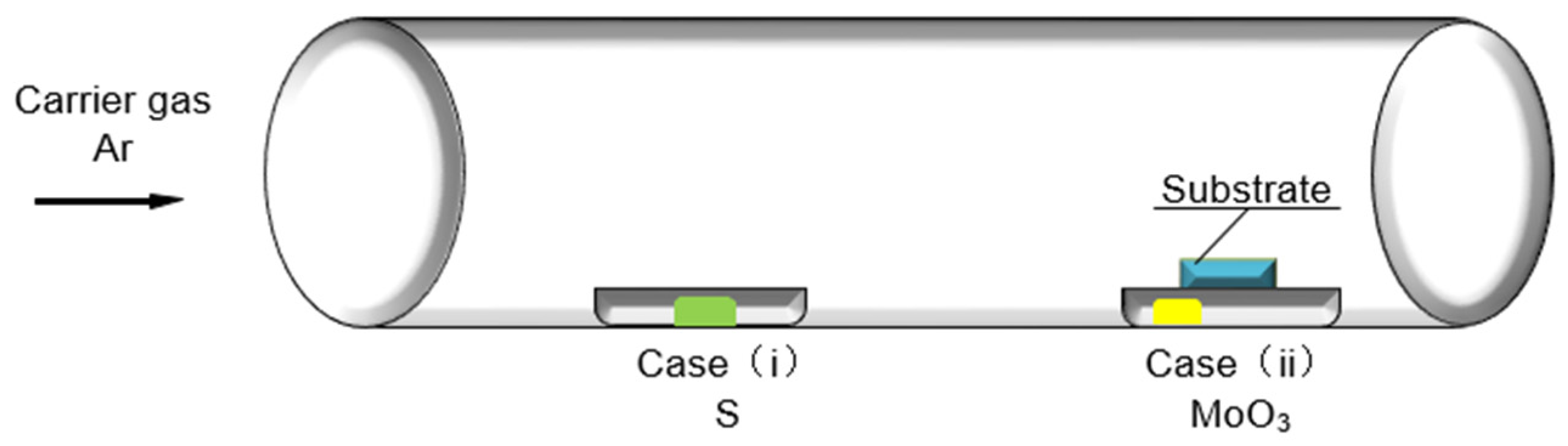
2. Experiments
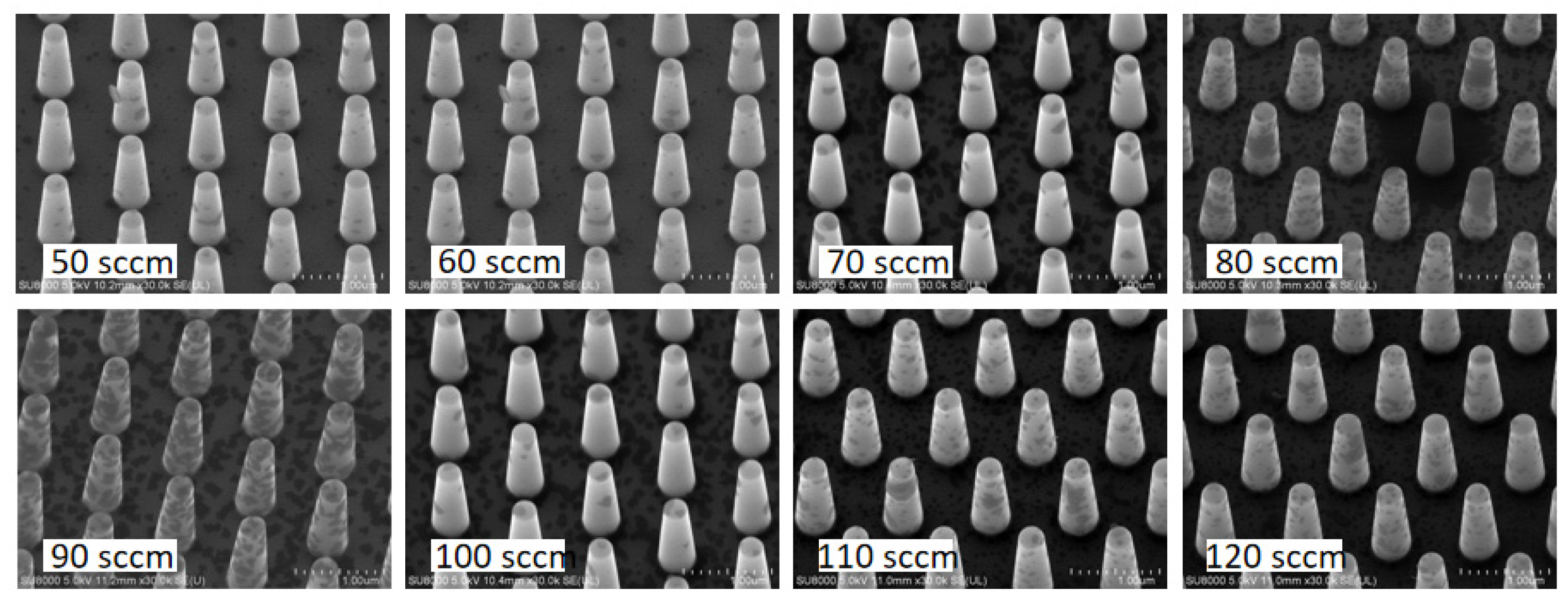
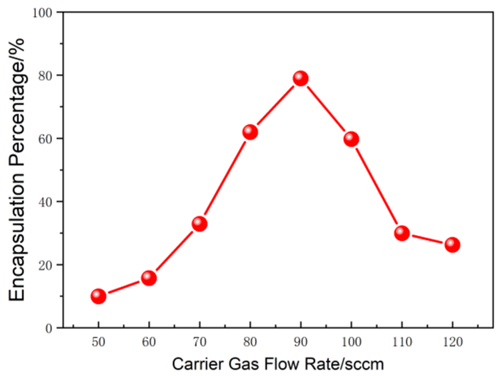
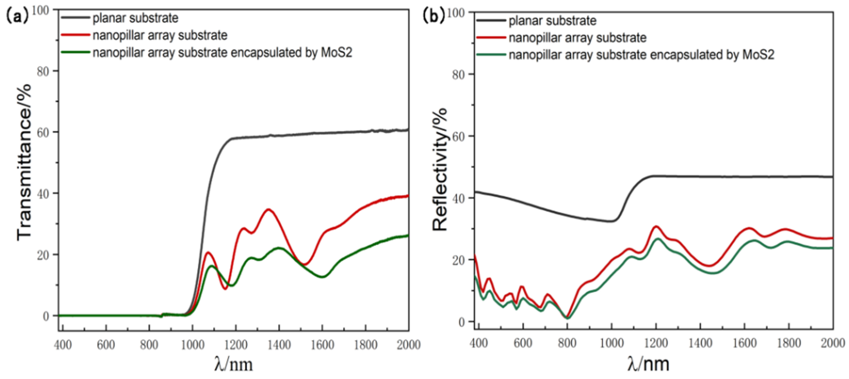
3. Results and Discussion
4. Conclusions
Author Contributions
Funding
Acknowledgments
Conflicts of Interest
References
- Susarla, S.; Kutana, A.; Hachtel, J.A.; Kochat, V.; Apte, A.; Vajtai, R.; Idrobo, J.C.; Yakobson, B.I.; Tiwary, C.S.; Ajayan, P.M. Quaternary 2D Transition Metal Dichalcogenides (TMDs) with tunable bandgap. Adv. Mater. 2017, 29, 1702457. [Google Scholar] [CrossRef]
- Hafeez, M.; Gan, L.; Bhatti, A.S.; Zhai, T. Rhenium dichalcogenides (ReX2, X = S or Se): An emerging class of TMDs family. Mater. Chem. Front. 2017, 1, 1917–1932. [Google Scholar] [CrossRef]
- Soares, D.M.; Mukherjee, S.; Singh, G. TMDs beyond MoS2 for electrochemical energy storage. Chem. Eur. J. 2020, 26, 6320–6341. [Google Scholar] [CrossRef] [PubMed]
- Zeng, B.; Huang, Z.; Singh, A.; Yao, Y.; Azad, A.K.; Mohite, A.D.; Taylor, A.J.; Smith, D.R.; Chen, H.-T. Hybrid graphene metasurfaces for high-speed mid-infrared light modulation and single-pixel imaging. Light Sci. Appl. 2018, 7, 1–8. [Google Scholar] [CrossRef] [PubMed]
- Chen, X.; Shehzad, K.; Gao, L.; Long, M.; Guo, H.; Qin, S.; Wang, X.; Wang, F.; Shi, Y.; Hu, W.; et al. Graphene hybrid structures for integrated and flexible optoelectronics. Adv. Mater. 2020, 32, 1902039. [Google Scholar] [CrossRef] [PubMed]
- Fang, C.; Liu, Y.; Han, G.; Shao, Y.; Huang, Y.; Zhang, J.; Hao, Y. Absorption enhancement for black phosphorus active layer based on plasmonic nanocavity. IEEE Photonics J. 2017, 9, 1–10. [Google Scholar] [CrossRef]
- Valdez-Sandoval, L.; Ramirez-Garcia, E.; Jimenez, D.; Pacheco-Sanchez, A. Contact resistance assessment and high-frequency performance projection of black phosphorus field-effect transistor technologies. Semicond. Sci. Technol. 2020, 35, 125016. [Google Scholar] [CrossRef]
- Sriram, P.; Manikandan, A.; Chuang, F.-C.; Chueh, Y.-L. Hybridizing plasmonic materials with 2D-transition metal dichalcogenides toward functional applications. Small 2020, 16, 1904271. [Google Scholar] [CrossRef]
- Bieniek, M.; Szulakowska, L.; Hawrylak, P. 2D materials for optoelectronic devices. In Proceedings of the 19th International Conference on Numerical Simulation of Optoelectronic Devices (NUSOD 2019), Ottawa, ON, Canada, 8–12 July 2019; Piprek, J., Hinzer, K., Eds.; pp. 113–114. [Google Scholar]
- Cheng, J.; Wang, C.; Zou, X.; Liao, L. Recent advances in optoelectronic devices based on 2D materials and their heterostructures. Adv. Opt. Mater. 2019, 7, 1800441. [Google Scholar] [CrossRef] [Green Version]
- Kang, S.; Lee, D.; Kim, J.; Capasso, A.; Kang, H.S.; Park, J.-W.; Lee, C.-H.; Lee, G.-H. 2D semiconducting materials for electronic and optoelectronic applications: Potential and challenge. 2D Mater. 2020, 7, 022003. [Google Scholar] [CrossRef]
- Ruiz, I.; Beechem, T.E.; Smith, S.; Dickens, P.; Paisley, E.A.; Shank, J.; Howell, S.W.; Sarma, R.; Draper, B.L.; Goldflam, M.D. Interface defect engineering for improved graphene-oxide-semiconductor junction photodetectors. ACS Appl. Nano Mater. 2019, 2, 6162–6168. [Google Scholar] [CrossRef]
- Anandan, M.; Hsieh, H.-F.; Liu, F.-C.; Chen, C.-Y.; Lee, K.-Y.; Chao, L.-C.; Ho, C.-H.; Chen, R.-S. High-responsivity broad-band sensing and photoconduction mechanism in direct-Gap alpha-In(2)Se(3)nanosheet photodetectors. Nanotechnology 2020, 31, 465201. [Google Scholar] [CrossRef] [PubMed]
- Bai, M.; Liu, H.; Xie, F.; Liu, W.; Wen, S. Improvement of two-dimensional material-based photodetector through surface plasmon. Int. J. Mod. Phys. B 2020, 34, 2050258. [Google Scholar] [CrossRef]
- Chen, Z.Y.; Mei, J.J.; Zhang, Y.; Tan, J.S.; Xiong, Q.; Chen, C.H. Interface phonon polariton coupling to enhance graphene absorption. Front. Optoelectron. 2019, 1–5. [Google Scholar] [CrossRef]
- Miao, J.; Hu, W.; Jing, Y.; Luo, W.; Liao, L.; Pan, A.; Wu, S.; Cheng, J.; Chen, X.; Lu, W. Surface plasmon-enhanced photodetection in few layer MoS2 phototransistors with Au nanostructure arrays. Small 2015, 11, 2392–2398. [Google Scholar] [CrossRef] [PubMed]
- Garoli, D.; Mosconi, D.; Miele, E.; Maccaferri, N.; Ardini, M.; Giovannini, G.; Dipalo, M.; Agnoli, S.; De Angelis, F. Hybrid plasmonic nanostructures based on controlled integration of MoS2 flakes on metallic nanoholes. Nanoscale 2018, 10, 17105–17111. [Google Scholar] [CrossRef] [PubMed] [Green Version]
- Camellini, A.; Mazzanti, A.; Mennucci, C.; Martella, C.; Lamperti, A.; Molle, A.; Buatier de Mongeot, F.; Della Valle, G.; Zavelani-Rossi, M. Evidence of plasmon enhanced charge transfer in large-area hybrid Au-MoS2 metasurface. Adv. Opt. Mater. 2020, 8, 2000653. [Google Scholar] [CrossRef]
- Deng, Y.S.; Wang, G.; Qiu, Y.; He, D.S.; Lin, J.H.; He, J.Q. Nano-patterning of a monolayer molybdenum disulfide with sub-nanometer helium ion beam: Considering its shape, size and damage. Nanotechnology 2020, 31, 6. [Google Scholar] [CrossRef]
- Furchi, M.; Urich, A.; Pospischil, A.; Lilley, G.; Unterrainer, K.; Detz, H.; Klang, P.; Andrews, A.M.; Schrenk, W.; Strasser, G.; et al. Microcavity-integrated graphene photodetector. Nano Lett. 2012, 12, 2773–2777. [Google Scholar] [CrossRef]
- Zhang, J.; Hong, Q.; Zou, J.; Meng, Q.; Qin, S.; Zhu, Z. Ultra-narrowband visible light absorption in a monolayer MoS2 based resonant nanostructure. Opt. Express 2020, 28, 27608–27614. [Google Scholar] [CrossRef]
- Chaliyawala, H.; Aggarwal, N.; Purohit, Z.; Patel, R.; Gupta, G.; Jaffre, A.; Le Gall, S.; Ray, A.; Mukhopadhyay, I. Role of nanowire length on the performance of a self-driven NIR photodetector based on mono/bi-layer graphene (camphor)/Si-nanowire Schottky junction. Nanotechnology 2020, 31, 225208. [Google Scholar] [CrossRef]
- Lu, J.; Yan, J.; Yao, J.; Zheng, Z.; Mao, B.; Zhao, Y.; Li, J. All-dielectric nanostructure fabry-perot-enhanced mie resonances coupled with photogain modulation toward ultrasensitive In2S3 photodetector. Adv. Funct. Mater. 2021, 31, 2007987. [Google Scholar] [CrossRef]
- Manzeli, S.; Ovchinnikov, D.; Pasquier, D.; Yazyev, O.V.; Kis, A. 2D transition metal dichalcogenides. Nat. Rev. Mater. 2017, 2, 1–15. [Google Scholar] [CrossRef]
- Eda, G.; Yamaguchi, H.; Voiry, D.; Fujita, T.; Chen, M.; Chhowalla, M. Photoluminescence from chemically exfoliated MoS2. Nano Lett. 2011, 11, 5111–5116. [Google Scholar] [CrossRef] [PubMed]
- Liu, K.-K.; Zhang, W.; Lee, Y.-H.; Lin, Y.-C.; Chang, M.-T.; Su, C.Y.; Chang, C.-S.; Li, H.; Shi, Y.; Zhang, H.; et al. Growth of large-area and highly crystalline MoS2 thin layers on insulating substrates. Nano Lett. 2012, 12, 1538–1544. [Google Scholar] [CrossRef] [PubMed] [Green Version]
- Donnelly, G.E.; Velicky, M.; Hendren, W.R.; Bowman, R.M.; Huang, F. Achieving extremely high optical contrast of atomically-thin MoS2. Nanotechnology 2020, 31, 145706. [Google Scholar] [CrossRef]
- Kim, D.; Jo, Y.; Jung, D.H.; Lee, J.S.; Kim, T. Electrical and optical characteristics of two-dimensional MoS2 film grown by metal-organic chemical vapor deposition. J. Nanosci. Nanotechnol. 2020, 20, 3563–3567. [Google Scholar] [CrossRef] [PubMed]
- Rajan, A.G.; Warner, J.H.; Blankschtein, D.; Strano, M.S. Generalized mechanistic model for the chemical vapor deposition of 2D transition metal dichalcogenide monolayers. ACS Nano 2016, 10, 4330–4344. [Google Scholar] [CrossRef]
- Tao, J.; Chai, J.; Lu, X.; Wong, L.M.; Wong, T.I.; Pan, J.; Xiong, Q.; Chi, D.; Wang, S. Growth of wafer-scale MoS2 monolayer by magnetron sputtering. Nanoscale 2015, 7, 2497–2503. [Google Scholar] [CrossRef] [PubMed]
- Bai, M.Y.; Liu, H.; Xie, F.; Zhao, J.J.; Liu, W.G.; Xie, H.K. Light trapping enhancement via structure design. Int. J. Mod. Phys. B 2020, 34, 10. [Google Scholar] [CrossRef]
- Bao, H.; Ruan, X. Optical absorption enhancement in disordered vertical silicon nanowire arrays for photovoltaic applications. Opt. Lett. 2010, 35, 3378–3380. [Google Scholar] [CrossRef] [PubMed]
- Cao, L.; Fan, P.; Vasudev, A.P.; White, J.S.; Yu, Z.; Cai, W.; Schuller, J.A.; Fan, S.; Brongersma, M.L. Semiconductor nanowire optical antenna solar absorbers. Nano Lett. 2010, 10, 439–445. [Google Scholar] [CrossRef] [PubMed]


Publisher’s Note: MDPI stays neutral with regard to jurisdictional claims in published maps and institutional affiliations. |
© 2021 by the authors. Licensee MDPI, Basel, Switzerland. This article is an open access article distributed under the terms and conditions of the Creative Commons Attribution (CC BY) license (http://creativecommons.org/licenses/by/4.0/).
Share and Cite
Bai, M.; Wang, Z.; Zhao, J.; Wen, S.; Zhang, P.; Xie, F.; Liu, H. 2D MoS2 Encapsulated Silicon Nanopillar Array with High-Performance Light Trapping Obtained by Direct CVD Process. Crystals 2021, 11, 267. https://doi.org/10.3390/cryst11030267
Bai M, Wang Z, Zhao J, Wen S, Zhang P, Xie F, Liu H. 2D MoS2 Encapsulated Silicon Nanopillar Array with High-Performance Light Trapping Obtained by Direct CVD Process. Crystals. 2021; 11(3):267. https://doi.org/10.3390/cryst11030267
Chicago/Turabian StyleBai, Minyu, Zhuoman Wang, Jijie Zhao, Shuai Wen, Peiru Zhang, Fei Xie, and Huan Liu. 2021. "2D MoS2 Encapsulated Silicon Nanopillar Array with High-Performance Light Trapping Obtained by Direct CVD Process" Crystals 11, no. 3: 267. https://doi.org/10.3390/cryst11030267
APA StyleBai, M., Wang, Z., Zhao, J., Wen, S., Zhang, P., Xie, F., & Liu, H. (2021). 2D MoS2 Encapsulated Silicon Nanopillar Array with High-Performance Light Trapping Obtained by Direct CVD Process. Crystals, 11(3), 267. https://doi.org/10.3390/cryst11030267