Article

Photocontrollable Resistivity Change in Nanoparticle-Doped Liquid Crystal Alignment Layer: Voltage Holding and Discharging Properties of Fringe-Field Switching Liquid Crystal Modes

1
School of Electronic and Electrical Engineering, Kyungpook National University, Daegu 41566, Korea
2
LG Display Co., Ltd., Paju, Gyeounggi-do 10845, Korea
3
Department of Sensor and Display Engineering, Kyungpook National University, Daegu 41566, Korea
4
School of Electronics Engineering, Kyungpook National University, Daegu 41566, Korea
*
Author to whom correspondence should be addressed.
These authors contributed equally to this work.
Crystals 2021, 11(3), 268; https://doi.org/10.3390/cryst11030268
Submission received: 18 February 2021 / Revised: 4 March 2021 / Accepted: 5 March 2021 / Published: 9 March 2021
(This article belongs to the Special Issue Organic Optoelectronic Materials (Volume II))

Abstract

:
In liquid crystal (LC) displays, deriving an optimum resistance level of an LC alignment polyimide (PI) layer is important because of the trade-off between the voltage holding and surface-discharging properties. In particular, to apply a power-saving low-frequency operation scheme to fringe-field switching (FFS) LC modes with negative dielectric LC (n-LC), delicate material engineering is required to avoid surface-charge-dependent image flickering and sticking problems, which severely degrade with lowering operation frequency. Therefore, this paper proposes a photocontrolled variable-resistivity PI layer in order to systematically investigate the voltage holding and discharging properties of the FFS n-LC modes, according to the PI resistivity (ρ) levels. By doping fullerene into the high-ρ PI as the photoexcited charge-generating nanoparticles, the ρ levels of the PI were continuously controllable with a wide tunable range (0.95 × 10¹⁵ Ω∙cm to 5.36 × 10¹³ Ω∙cm) through Ar laser irradiation under the same LC and LC alignment conditions. The frequency-dependent voltage holding and discharge behaviors were analyzed with photocontrolled ρ variation. Thus, the proposed experimental scheme is a feasible approach in PI engineering for a power-saving low-frequency FFS n-LC mode without the image flickering and image sticking issues.

1. Introduction

Fringe-field switching (FFS) liquid crystal (LC) modes are widely applied to mobile display applications as the most competitive LC operation scheme, owing to their high optical efficiency and low power consumption [1,2,3]. To satisfy the recent display technology requirements of higher pixel resolution, LCs with a negative dielectric anisotropy (n-LCs) are being more actively applied to FFS LC modes than conventional positive dielectric anisotropy LCs (p-LCs), because field-induced LC reorientations in the FFS n-LC mode occur dominantly along the horizontal direction with a more effective pixel aperture ratio compared to the FFS p-LC mode, which exhibits periodic vertical LC reorientations under the applied fringe fields [1,4,5]. However, with increasing pixel density, the mobile display panels suffer from power consumption issues. Because the power consumption level in driving circuits is proportional to the operation frequency [6,7], extensive efforts have been made to reduce the operation frequency level of FFS LC modes without degrading the image quality [8,9,10,11,12,13,14,15,16].
In reducing the operation frequency level, the FFS n-LC modes are superior to FFS p-LC modes, as the dynamic flexoelectric LC effects coupled with image flickering can be relatively reduced in the FFS n-LC modes [5,17,18,19]. However, the relatively abundant bulk ionic charges within n-LCs make the charge drift along the applied fringe field direction, which gradually reduces the effective field amount within the FFS n-LC cells due to the increased surface-accumulated charges during the time duration applied with the same signal voltage polarity condition [20,21,22]. The charge accumulation effects by the movable ions within the n-LCs induce gradually decreasing behavior in terms of brightness level during the same signal voltage polarity duration, and abrupt brightness level changes at the moment of signal voltage polarity inversion, causing frequency-dependent voltage holding issues which are observable as image flickering problems. Moreover, the LC bulk charge density is highly dependent on the type of LC alignment polyimide (PI) layer applied to the FFS n-LC modes [20,22]. To improve the voltage holding property at a lower operation frequency, high-resistivity (ρ) PIs are more appropriate as an LC alignment layer because of their lower inherent ion impurity levels and lower ion desorption characteristics, which are responsible for the alternative current (AC) operation of LC switching fields [20]. However, in case of image sticking issues, i.e., whereby the previous frame image is still observed as a faint outline due to surface-accumulated charge effects even after the display image has changed, high-resistivity PIs are more vulnerable [23,24]. Image sticking occurs due to charges which have accumulated at the interface between the LC and the PI layer by the positional variation of the offset voltage level and the dielectric imperfection [25,26,27]. To avoid this issue, surface-accumulated charges need to be quickly discharged. For this purpose, a lower resistivity condition of PIs is more desirable [23,24]. Both voltage holding and surface-discharging properties are highly dependent on the PI resistivity level with a trade-off relation. To develop power-saving FFS n-LC modes operable at sufficiently low-frequency levels without the image flickering and image sticking issues, the voltage holding and discharging properties must be systematically investigated according to the PI resistivity level.
In this study, we present a photocontrolled ρ-variable LC alignment PI layer in order to systematically investigate the voltage holding and discharging properties in the FFS n-LC modes. By doping fullerenes into the high-ρ PI layer as the photoexcited charge generation nanoparticles, and by controlling the irradiation intensity of the Ar laser, the resistivity level of the PI can be widely tuned from 0.95 × 10¹⁵ Ω∙cm to 5.36 × 10¹³ Ω∙cm, even at a low concentrations (0.05 wt%) of fullerene doping. By applying the photocontrolled ρ-variable PI layer to the FFS n-LC mode, the frequency-dependent temporal transmittance properties and dynamic residual voltage curves are measured according to the photocontrolled resistivity variation, and the trade-off relationship between the frequency-dependent voltage holding ratios (VHRs) and the surface-discharging coefficients may be analyzed based on the measurement results. The proposed experimental scheme is a feasible approach in the delicate material engineering of LC alignment PI layers required to resolve PI-dependent image flickering and sticking issues occurring in low-frequency-driven FFS n-LC modes adopted for power saving operation in mobile display panels.

2. Materials and Methods

Figure 1 shows a schematic of the cross-sectional device structure of the FFS n-LC mode used in our experiment, where a photocontrolled ρ-variable LC alignment PI layer was added on the bottom substrate. This substrate comprises two indium-tin-oxide electrodes (a stripe-patterned pixel electrode and a nonpatterned common electrode), where the width and spacing of the pixel electrode were 3 μm and 4 μm, respectively. Between the two electrodes, a 500 nm-thick dielectric layer (SiNx, ρ ~ 1014 Ω∙cm) was deposited to generate fringe fields. With these electrodes and dielectric structure, fine fringe field patterns are generated within the n-LC layer, which gives rise to a field-induced horizontally reoriented LC distribution, thereby avoiding highly distorted LC distribution and highly increased elastic LC energies [5]. The field-induced LC reorientation along the horizontal plane in the FFS n-LC mode is advantageous in achieving a higher transmittance level compared with the FFS p-LC mode exhibiting the field-induced LC reorientation along the fringe field direction. On the top substrate, black-matrix patterns were formed at each pixel boundary and the planar-anchoring LC alignment PI layer was spin-coated without electrode deposition. Both PI layers were rubbed with a rubbing cloth in a direction of 7° with respect to the striped pattern of the pixel electrode to determine the initial LC alignment direction. Furthermore, 4 μm-diameter ball spacers were used to obtain a uniform cell gap; then, n-LC material (ML1407, Merck, Germany) was injected into the prepared LC cells. The physical properties of the n-LC material were as follows: dielectric anisotropy of Δε = −4.1; birefringence of Δn = 0.1011; elastic LC constants of K11 = 13.3 pN, K22 = 6.7 pN, K33 = 15.1 pN.
As the LC alignment layer, a high-ρ PI (ρ ~ 1015 Ω∙cm, AL16470, Japan Synthetic Rubber Co., Japan) was used. For the photocontrolled ρ-variable PI used in the bottom substrate, a mixed solution of PI and fullerene nanoparticles was prepared by varying the mixing ratio. As the photoinduced charge generation nanoparticles [28,29,30], chemically modified fullerene nanoparticles ([6,6]-phenyl-C71 butyric acid methyl ester, American Dye Source) were used. Before the doping process, the fullerene nanoparticles were heat-treated in a vacuum oven at 200 °C for four hours to remove moisture from their surfaces. The prepared mixture solution was then subjected to an ultrasonic treatment under the conditions of 46 kHz, 150 W, and 0 °C for 1 h to obtain a homogenous mixture. The spin-coated PI layers were prebaked at 80 °C for 60 s to remove the solvent and then polymerized by the postbaking process performed at 250 °C for 30 min.
Figure 2 shows the experimental setup for characterizing the dynamic voltage holding and surface-discharging properties of the FFS n-LC mode with optically varying resistivity level of the LC alignment layer. Considering the absorption wavelength peaks of the fullerene nanoparticles doped into the high-ρ PI existing near 373 nm and 463 nm wavelengths [28,29,30], an Ar laser (λ = 488 nm) was used as an excitation beam for the photocontrolled charge generation. In addition, a He–Ne laser (λ = 633 nm) was used as a probing light source for characterizing the electro-optic properties of the FFS n-LC cells. Using a signal generator (33500B, Keysight Technologies Inc., Santa Rosa, CA, USA), the operation signal voltages were directly applied to the FFS n-LC mode under varying operation frequencies. To measure the electro-optic dynamics of the FFS n-LC cells placed between the crossed polarizers, a photodetector (Model 2031, Newport Inc., Irvine, CA, USA) and an oscilloscope (DSO1052B, Keysight Technologies Inc., Santa Rosa, CA, USA) were used, where the signal measured by the oscilloscope was synchronized with the waveform of the AC signal applied by the signal generator.

3. Results and Discussion

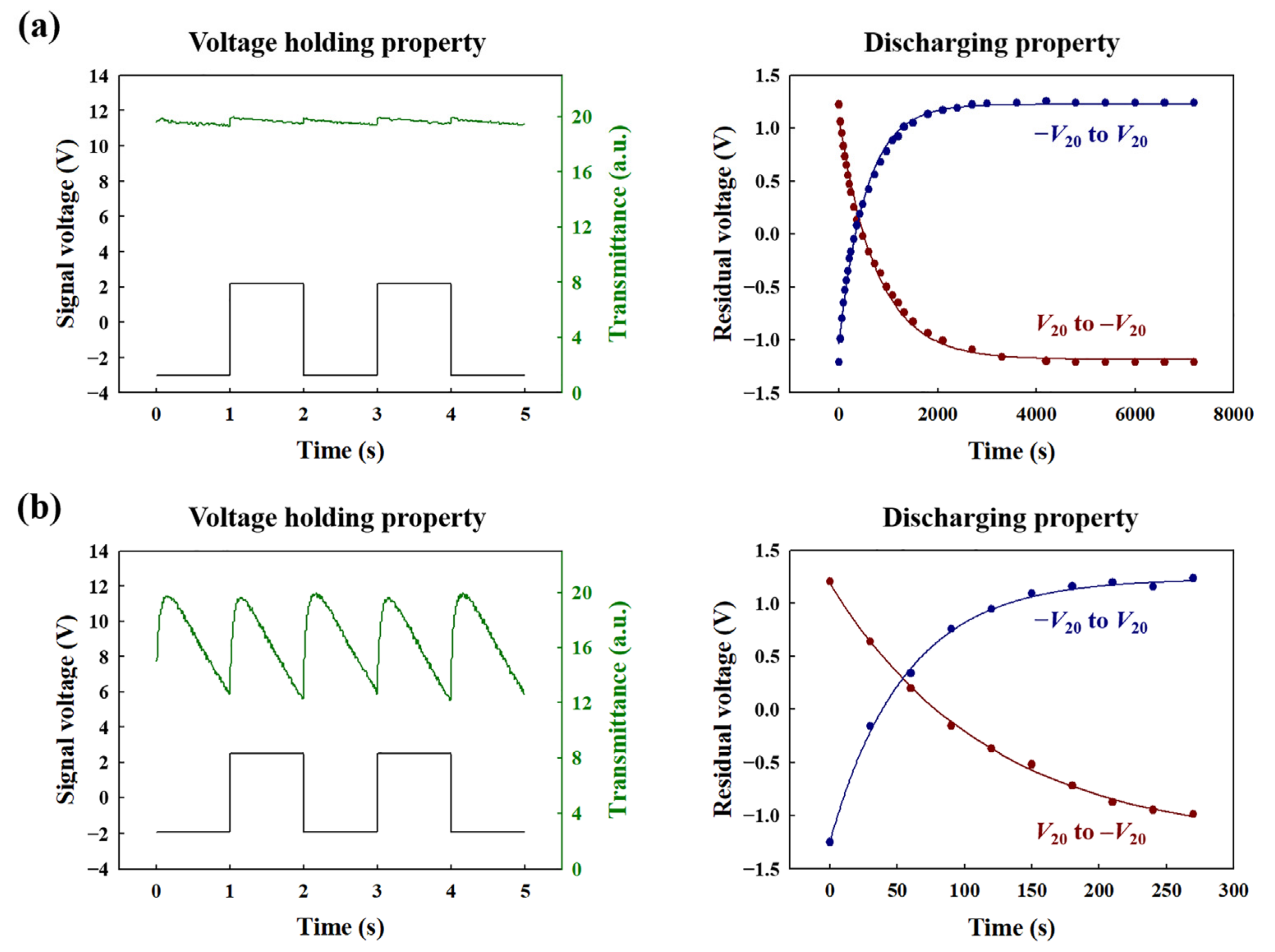
3.1. Voltage Holding and Discharging Properties According to PI Resistivity

Before applying the photocontrolled ρ-variable LC alignment PI layer to the FFS n-LC mode, the voltage holding and surface-discharging properties of the FFS n-LC mode were characterized using two types of commercial LC alignment PIs in terms of resistivity levels without fullerene doping: a high-ρ PI (ρ ~ 1015 Ω∙cm, AL16470, Japan Synthetic Rubber Co., Japan) and a low-ρ PI (ρ ~ 1013 Ω∙cm, SE6514, Nissan Chemical Co., Japan). The high-ρ PI used in our experiment was an LC alignment PI material synthesized to reduce the inner impurity level and to suppress the charge desorption behaviors. Figure 3 presents the temporal transmittance and residual voltage curves of two types of FFS n-LC cells, where a typical trade-off between the voltage holding and surface-discharging properties is observed depending on the resistivity properties of the PIs. As the frequency-dependent voltage holding properties, the temporal transmittance curves obtained at a 0.5 Hz signal voltage frequency, for example, are presented. Square-wave AC signals were applied to both types of FFS n-LC cells, where the signal voltage amplitude (V20) required for a transmittance level of 20% of the maximum brightness level was applied [12]. The voltage level of V20 corresponds to the intermediate gray level on the gamma 2.2 grayscale curve, which is commonly used to evaluate the image flickering characteristics considering human gamma sensitivity [12]. Furthermore, to minimize the maximum transmittance level variation according to the polarity changes of the AC signal voltage in evaluating the voltage holding properties, an optimum DC offset level was found and applied to each FFS n-LC cell. From the temporal transmittance curves, the VHR properties can be characterized as follows [20,25]:
V H R = ( T min / T max ) × 100
where Tmin and Tmax indicate the minimum and maximum transmittance levels, respectively, in the periodic transmittance fluctuations in response to the signal polarity changes. In characterizing the discharging properties from the measured residual voltage curves, each FFS n-LC cell was sufficiently prebiased by a DC voltage (at the positive or negative polarity of the V20 level) for a long time until the transmittance level became saturated by the surface-accumulated charges. Then, by applying an opposite-polarity field of the DC voltage, the residual voltage curves, which were time-varying with surface-discharging, were obtained, as shown in Figure 3. For a quantitative analysis and comparison of the discharging properties according to the PI types, the discharging coefficients of α (s−1) were evaluated by fitting the dynamic residual voltage curves [20,25]:
V r ( t ) = V r s a t + ( V s a t V r s a t ) e α t
where Vr is the time-varying residual voltage, Vsat is the saturation voltage by the prebiased field, and Vrsat is the reverse saturation voltage with discharging after the signal voltage polarity change.
When the FFS n-LC cell adopted a high-ρ PI, relatively better VHR characteristics (98.11%) were obtained under the 0.5 Hz operation. However, the extracted α value was too low (0.002 s−1) to discharge the accumulated charges. Thus, the high-ρ PI could not function effectively as a discharge path layer for the accumulated charges within the PI, which suffered from the image sticking problem. In contrast, by adopting a low-ρ PI, the discharging property was much improved, i.e., by α = 0.009 s−1, whereas the voltage holding characteristics were severely degraded, i.e., VHR = 63.10%. This high fluctuation in the temporal brightness level occurring during signal polarity changes made the image flickering observable by human eyes. Considering human sensitivity to image flickering [10,11], the VHR levels required to prevent image flickering noticeable by human eyes are highly dependent on the fluctuation frequency of the brightness levels. The results of Figure 3 clearly show that the frequency-dependent voltage holding and discharging properties are highly dependent on the resistivity level of the employed PI layer with a trade-off relation. In developing the low-frequency-driven FFS n-LC modes free from the image flickering and image sticking issues, the photocontrolled ρ-variable LC alignment PI layer enables the characterization of the VHR and discharging coefficient under the same LC and host PI material combination conditions with varying PI resistivity levels, which provides an efficient investigation route for systematic material engineering.

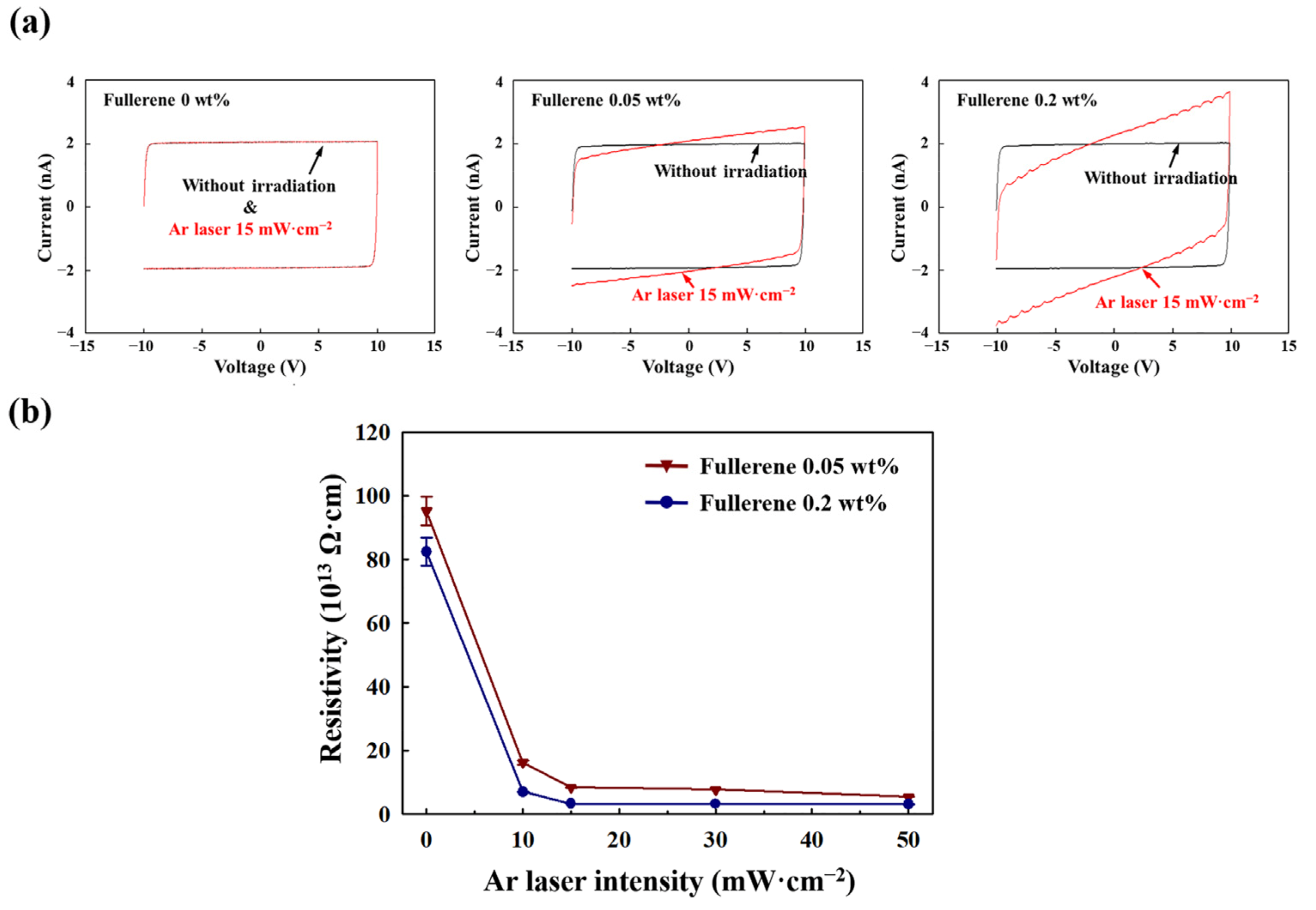
3.2. Photocontrollable Resistivity Changes in Fullerene-Doped High-ρ PI Layer

To obtain the optimum fullerene doping density condition as the photocontrolled ρ-variable LC alignment PI layer applicable to the FFS n-LC mode investigation, the achievable ranges of specific resistivity variation of the fullerene-doped high-ρ PI layer were characterized at different fullerene doping concentrations and under different Ar laser irradiation conditions, as shown in Figure 4. For an effective PI layer defined by the patterned Al electrodes, the relation between the current (I) and applied voltage (V) was evaluated using the precision source-measurement units (B2901A, Keysight Technologies Inc., Santa Rosa, CA, USA).
In the pristine high-ρ PI without fullerene doping, the VI curves were identical irrespective of the application of Ar laser irradiation with the highest resistivity level of 1.44 × 10¹⁵ Ω∙cm. However, in case of fullerene doping, the slopes of the VI curves obtained in the presence of Ar laser irradiation (15 mW∙cm−2) increased with fullerene doping concentrations employed as photocontrolled charge generation nanoparticles. Figure 4b summarizes the photocontrolled PI resistivity values extracted from the VI curve measurements according to the fullerene doping concentrations and Ar laser irradiation intensity. Without the Ar laser irradiation, the specific resistivity values of the fullerene-doped PIs decreased with increasing fullerene doping concentration: ρ = 1.44 × 10¹⁵ Ω∙cm at 0 wt%, ρ = 0.95 × 10¹⁵ Ω∙cm at 0.05 wt%, and ρ = 0.83 × 10¹⁵ Ω∙cm at 0.2 wt%. This is attributable to the fact that the ionic impurities increased during fullerene doping because the purchased fullerenes were used without additional purification in our experiment. In addition, the specific resistivity conditions of the fullerene-doped PIs were effectively varied by controlling the Ar laser irradiation intensity, with their values decreasing drastically, even under a weak Ar irradiation condition (10 mW∙cm−2): ρ = 1.61 × 10¹⁴ Ω∙cm at 0.05 wt% and ρ = 6.92 × 10¹³ Ω∙cm at 0.2 wt%. In our experiment, under an Ar irradiation of 50 mW∙cm−2, the specific resistivity conditions of the fullerene-doped PIs could be decreased to ρ = 5.36 × 10¹³ Ω∙cm at 0.05 wt% and ρ = 3.06 × 10¹³ Ω∙cm at 0.2 wt% through the photoexcited charge generation.
Considering the achievable tunable range of the photocontrolled specific resistivity values, the fullerene doping concentration of 0.05 wt% was selected for the photocontrolled ρ-variable LC alignment PI layer used for investigating the voltage holding and surface-discharging properties with preparation of the FFS n-LC cells. The photocontrolled specific resistivity value of the fullerene-doped high-ρ PI obtained at an Ar irradiation of 50 mW∙cm−2 and doping concentration of 0.05 wt% was slightly lower than that (ρ = 6.63 × 10¹³ Ω∙cm) of the pristine low-ρ PI without fullerene doping. The specific resistivity of the proposed fullerene-doped PI can be continuously varied by Ar laser irradiation from those of the high-ρ PIs to those of the low-ρ PIs under the same PI material conditions.

3.3. Discharging Properties by Residual Voltage Dynamics

Figure 5a shows the dynamic residual voltage curves of the FFS n-LC cell with 0.05 wt% fullerene-doped high-ρ PI layer under the Ar laser irradiation intensity conditions. In case of using the fullerene-doped high-ρ PI without Ar laser irradiation, the residual voltage takes considerable time to change from Vsat to Vrsat, which means that the surface-accumulated charges are discharged very slowly. When the Ar laser irradiated the FFS n-LC cell, with an improvement in the discharging properties, the dynamic residual voltage curves changed more steeply compared to those without Ar laser irradiation. As shown in the inset graphs of Figure 5a, the dynamic residual voltage curves became gradually steeper with increasing Ar laser intensity.
According to the dynamic residual voltage curves shown in Figure 5a, the discharging coefficients of the FFS n-LC mode with the photocontrolled ρ-variable LC alignment PI layer (fullerene doping concentration: 0.05 wt%) were evaluated under the Ar laser intensity conditions to quantitatively compare and analyze the discharging properties of the FFS n-LC mode. Figure 5b coplots the photocontrolled conductivity values of the fullerene-doped high-ρ PI, which were calculated from the results of Figure 4b. As shown in the figure, the photocontrolled behaviors of the discharging coefficient could be monotonically increased under a wide tunable range of α = 0.003 s−1 to 0.039 s−1, which coincides well with the photocontrolled conductivity curve of the fullerene-doped high-ρ PI.

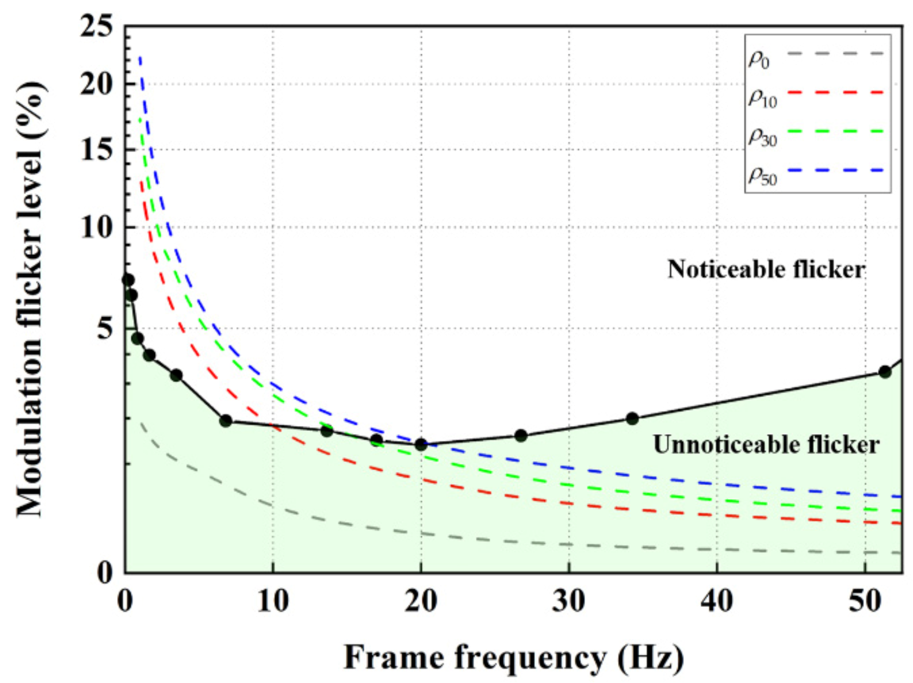
3.4. Frequency-Dependent Voltage Holding Properties

Figure 6a shows the frequency-dependent temporal transmittance variation of the FFS n-LC cell (fullerene doping concentration within the high-ρ PI: 0.05 wt%) obtained without or with Ar laser irradiation. In this experiment, the Ar laser intensity was fixed at 50 mW∙cm−2 and the operation frequency of the signal voltage waveform was varied from 0.5 Hz to 0.2 Hz. In all cases, the transmittance variation gradually decreased before the signal polarity inversion because the effective voltage levels applied to the FFS n-LC cell exhibited time-varying decreasing behavior due to the bulk ion drift within the n-LC cell and the charge desorption and subsequent re-adsorption at the PI surface. Compared with the temporal transmittance curves without Ar laser irradiation, the transmittance fluctuations became more severe under Ar laser irradiation because of the photoinduced increased charge transfer from the fullerene-doped PI layer.
Figure 6b shows the frequency-dependent VHR characteristics of the FFS n-LC mode with the photocontrolled ρ-variable LC alignment PI layer, which were evaluated from the temporal transmittance variation curves shown in Figure 6a. Without Ar laser irradiation, a VHR level of 96.17% was achieved at 0.5 Hz operation frequency, which gradually degraded until reaching the value of 90.91% at 0.2 Hz. With Ar laser irradiation (50 mW∙cm−2), the VHR level was severely degraded compared to that without Ar laser irradiation, i.e., from VHR = 63.65% at 0.5 Hz to VHR = 42.80% at 0.2 Hz. This was attributed to the higher charge desorption and re-adsorption rates obtained for the fullerene-doped PI variable from a high-ρ PI to a low-ρ PI through photoinduced charge generation.
Figure 7 coplots the voltage holding (the signal voltage frequency: 0.5 Hz) and surface-discharging properties of the FFS n-LC cell (the fullerene doping density within the high-ρ PI: 0.05 wt%) obtained by varying the Ar laser irradiation condition. Among the various PI properties required in low-frequency-driven FFS n-LC mode, the PI resistivity level substantially affects the voltage holding and surface-discharging properties with a trade-off relation. When we compare the discharging capabilities of the photocontrolled PI with those of the commercial low-ρ PI, the discharging coefficient value obtained without the Ar laser irradiation was lower than the discharging coefficient level of the low-ρ PI (the dashed red line in Figure 7), which indicates that the resistivity level without the Ar laser irradiation is not free from the image sticking issue. However, the discharging coefficient values of the photocontrolled PI obtained with the Ar laser irradiation over 10 mW∙cm−2 were higher than those of the low-ρ PI, and those discharging capabilities became better with increasing the Ar laser irradiation intensity due to the effective photo-induced resistivity reduction of the fullerene-doped high-ρ PI.
The discharging coefficients are independent of the signal frequency level. On the other hand, the VHRs are highly dependent on the operation frequency condition, with gradually decreasing behaviors with decreasing frequency at the same PI resistivity condition. In addition, brightness level fluctuations perceivable by human eyes as image flickering are also dependent on the implemented frame frequency condition [11,31]. To examine the phenomenon of image flickering due to the photocontrolled resistivity condition, with consideration of the dynamic visual sensitivity properties, the frequency-dependent modulation flicker level (MFL) curves of the FFS n-LC cell prepared with the fullerene-doped high-ρ PI were evaluated by varying the Ar laser irradiation as follows [31]:
MFL = ( T max T min ) 2 / ( T max + T min ) 2 × 100
In Figure 8, the frequency-dependent MFL curves (the dashed lines) obtained with the photocontrolled ρ-variable PI are coplotted with the frequency-dependent modulation flicker threshold curve (the black solid line) [31] for comparison. The modulation flicker threshold level indicates the MFL amount where humans begin to perceive image flickering, considering dynamic visual sensitivity properties. These frequency-dependent threshold levels were obtained under the 2600 Td time-averaged luminance with the 2° field size condition. Without the Ar laser irradiation, the resistivity condition of the fullerene-doped high-ρ PI was sufficiently high with the superior VHR property, as shown in Figure 6b, and their MFL values were also below the perceivable threshold conditions without causing the image flickering problems over the whole frequency range in our evaluation with the V20 signal voltage level. However, as shown in Figure 7, such a high PI resistivity condition is not appropriate for the FFS n-LC cell considering the image sticking issue. With decreasing the PI resistivity levels by increasing the Ar laser irradiation intensity, the MFL values increased due to the decreasing VHR properties, which shifted the ρ–dependent crossover points between the MFL evaluation curves and the modulation flicker threshold curve toward the higher frame frequency condition. At an Ar laser irradiation intensity of 10 mW∙cm−2 (ρ10 = 1.61 × 10¹⁴ Ω∙cm), perceivable image flickering occurred at about 10 Hz of the frame frequency condition. However, at 50 mW∙cm−2 of Ar irradiation (ρ50 = 5.36 × 10¹³ Ω∙cm), the frame frequency condition needed to be increased to about 20 Hz level to avoid image flickering.

4. Conclusions

This paper presents an optical ρ-variable PI layer, achieved by doping photoinduced charge generation fullerenes into a high-ρ LC alignment PI, in order to systematically investigate the trade-off between the voltage holding and discharging properties in the low-frequency-driven FFS n-LC modes. Even though a small concentration of fullerenes (0.05 wt%) was doped in the single-host high-ρ PI, the resistivity level of the optically modulated PI varied from ρ = 0.95 × 10¹⁵ Ω∙cm to ρ = 5.36 × 10¹³ Ω∙cm within a wide tunable range by controlling the Ar laser irradiation intensity. With the photocontrolled ρ-variable LC alignment PI layer, the frequency-dependent VHRs and discharging coefficients of the FFS n-LC cell were analyzed through a quantitative comparison according to the PI resistivity variation. The photocontrolled discharging coefficient showed a tunable range from α = 0.003 s−1 without Ar irradiation to α = 0.039 s−1 with Ar irradiation (50 mW∙cm−2 intensity). Moreover, the photocontrolled VHR exhibited a wide variation depending on the Ar laser irradiation intensity, i.e., from 96.17% without Ar irradiation to 63.65% with it (50 mW∙cm−2 intensity) at an operation frequency of 0.5 Hz. Under a fixed Ar irradiation intensity (50 mW∙cm−2 intensity), the voltage holding properties were also dependent on the operation frequency with degrading behavior from VHR = 63.65% at 0.5 Hz to 42.80% at 0.2 Hz. Thus, the proposed experimental scheme is expected to provide better systematic approaches for the design and synthesis of new types of PI materials for low-frequency-driven FFS n-LC modes without the image flickering and image sticking issues, especially when considering highly ρ-dependent voltage and discharging properties.

Author Contributions

Conceptualization, J.-H.K., J.-C.C., D.-J.L. and H.-R.K.; Investigation, J.-H.K., J.-C.C., D.-J.L., J.-W.L.; Supervision, H.-R.K.; Writing – original draft, J.-H.K., J.-C.C. and H.-R.K. All authors have read and agreed to the published version of the manuscript.

Funding

This work was supported by the National Research Foundation of Korea (NRF) grant funded by the Korea government (MSIT) (2019R1A2C1005531).

Conflicts of Interest

The authors declare no conflict of interest.

References

  1. Lee, S.H.; Lee, S.L.; Kim, H.Y. Electro-optic characteristics and switching principle of a nematic liquid crystal cell controlled by fringe-field switching. Appl. Phys. Lett. 1998, 73, 2881–2883. [Google Scholar] [CrossRef]
  2. Lee, S.H.; Kim, H.Y.; Lee, S.M.; Hong, S.H.; Kim, J.M.; Koh, J.W.; Lee, J.Y.; Park, H.S. Ultra-FFS TFT-LCD with super image quality, fast response time, and strong pressure-resistant characteristics. J. Soc. Inf. Disp. 2002, 10, 117–122. [Google Scholar] [CrossRef]
  3. Kim, D.H.; Lim, Y.J.; Kim, D.E.; Ren, H.; Ahn, S.H. Past, present, and future of fringe-field switching-liquid crystal display. J. Inf. Disp. 2014, 15, 99–106. [Google Scholar] [CrossRef] [Green Version]
  4. Kim, H.; Lee, J.H. Fast falling time of fringe-field switching negative dielectric anisotropy liquid crystal achieved by inserting vertical walls. Appl. Opt. 2015, 54, 1046–1050. [Google Scholar] [CrossRef]
  5. Yun, H.J.; Jo, M.H.; Jang, I.W.; Lee, S.H.; Ahn, S.H.; Hur, H.J. Achieving high light efficiency and fast response time in fringe field switching mode using a liquid crystal with negative dielectric anisotropy. Liq. Cryst. 2012, 39, 1141–1148. [Google Scholar] [CrossRef]
  6. Kim, T.S.; Kwa, S. 22.1: Invited Papers: Challenges and requirements of power saving techniques on mobile platforms. SID Symp. Dig. Tech. Pap. 2014, 45, 275–278. [Google Scholar] [CrossRef]
  7. You, B.H.; Nam, H.; Lee, H.J. 46-3: Image Adaptive Refresh Rate technology for Ultra Low Power Consumption. SID Symp. Dig. Tech. Pap. 2020, 51, 676–679. [Google Scholar] [CrossRef]
  8. Kim, M.; Jin, H.S.; Lee, S.J.; Shin, Y.H.; Ham, H.G.; Yang, D.K.; Bos, P.J.; Lee, J.H.; Lee, S.H. Liquid crystals for superior electro-optic performance display device with power-saving mode. Adv. Opt. Mater. 2018, 6, 1800022. [Google Scholar] [CrossRef]
  9. Tsuruma, T.; Goto, Y.; Higashi, A.; Watanabe, M.; Yamaguchi, H.; Tomooka, T.; Kikkawa, H. Novel image sticking model in the fringe field switching mode based on the flexoelectric effect. In Proceedings of the 31st International Display Research Conference 2011 (EuroDisplay 2011), Arcachon, France, 19–22 September 2011; Curran Associates, Inc.: Red Hook, NY, USA, 2011; pp. 15–18. [Google Scholar]
  10. Hatsumi, R.; Fukai, S.; Kubota, Y.; Yamashita, A.; Jikumaru, M.; Baba, H.; Moriya, K.; Kubota, D.; Kusunoki, K.; Hirakata, Y.; et al. FFS-mode OS-LCD for reducing eye strain. J. Soc. Inf. Disp. 2013, 21, 442–450. [Google Scholar] [CrossRef]
  11. Chen, H.; Peng, F.; Hu, M.; Wu, S.T. Flexoelectric effect and human eye perception on the image flickering of a liquid crystal display. Liq. Cryst. 2015, 42, 1730–1737. [Google Scholar] [CrossRef]
  12. Lee, D.J.; Shim, G.Y.; Choi, J.C.; Park, J.S.; Lee, J.H.; Baek, J.H.; Choi, H.C.; Ha, Y.M.; Ranjkesh, A.; Kim, H.R. Transient flickering behavior in fringe-field switching liquid crystal mode analyzed by positional asymmetric flexoelectric dynamics. Opt. Express 2015, 23, 34055–34070. [Google Scholar] [CrossRef]
  13. Kim, J.W.; Choi, T.H.; Yoon, T.H.; Choi, E.J.; Lee, J.H. Elimination of image flicker in fringe-field switching liquid crystal display driven with low frequency electric field. Opt. Express 2014, 22, 30586–30591. [Google Scholar] [CrossRef]
  14. Choi, H.S.; Kim, J.H.; Ham, H.G.; Lim, Y.J.; Lee, J.M.; Jin, H.S.; Manda, R.; Kim, M.S.; Yang, D.K.; Lee, S.H. P-131: Studies on flickering in low frequency driven fringe-field switching (FFS) liquid crystal display. SID Symp. Dig. Tech. Pap. 2016, 47, 1610. [Google Scholar] [CrossRef]
  15. Oh, S.W.; Park, J.H.; Lee, J.H.; Yoon, T.H. Elimination of image flicker in a fringe-field switching liquid crystal display by applying a bipolar voltage wave. Opt. Express 2015, 23, 24013–24018. [Google Scholar] [CrossRef] [PubMed]
  16. Kim, M.S.; Bos, P.J.; Kim, D.W.; Keum, C.M.; Yang, D.K.; Ham, H.G.; Jeong, K.U.; Lee, J.H.; Lee, S.H. Field-symmetrization to solve luminance deviation between frames in a low-frequency-driven fringe-field switching liquid crystal cell. Opt. Express 2016, 24, 29568–29576. [Google Scholar] [CrossRef]
  17. Lee, H.J.; Kim, H.M.; Kim, J.Y.; Lee, J.H. Dependence of image flickering of negative dielectric anisotropy liquid crystal on the flexoelectric coefficient ratio and the interdigitated electrode structure. J. Phys. D Appl. Phys. 2016, 49, 075501. [Google Scholar] [CrossRef]
  18. Chen, Y.; Luo, Z.; Peng, F.; Wu, S.T. Fringe-field switching with a negative dielectric anisotropy liquid crystal. J. Disp. Technol. 2013, 9, 74–77. [Google Scholar] [CrossRef] [Green Version]
  19. Chen, Y.; Peng, F.; Yamaguchi, T.; Song, X.; Wu, S.T. High performance negative dielectric anisotropy liquid crystals for display applications. Crystals 2013, 3, 483–503. [Google Scholar] [CrossRef] [Green Version]
  20. Kim, D.H.; Kim, J.H.; Kwon, Y.R.; Ahn, S.H.; Srivastava, A.K.; Lee, S.H. Investigation on ion movement in the fringe-field switching mode depending on resistivity of alignment layer and dielectric anisotropic sign of liquid crystal. Liq. Cryst. 2015, 42, 486–491. [Google Scholar] [CrossRef]
  21. Yoon, S.S.; Ahn, S.H.; Choi, W.Y.; Lee, J.H.; Kim, H.S.; Jun, M.C.; Kang, I.B. The study on DC resistibility of positive and negative dielectric anisotropy liquid crystal in AH-IPS mode. Dig. Tech. Pap. Soc. Inf. Disp. Int. Symp. 2016, 47, 1697–1699. [Google Scholar] [CrossRef]
  22. Choi, J.C.; Lee, D.J.; Park, M.K.; Park, J.S.; Lee, J.H.; Baek, J.H.; Choi, H.C.; Kim, H.R. Highly enhanced voltage holding property for low-frequency-driven fringe-field switching liquid crystal mode by charge-trapping effect of carbon-nanotube-doped surface. Opt. Express 2019, 27, 29178–29195. [Google Scholar] [CrossRef]
  23. Tsutsui, K.; Sakai, T.; Goto, K.; Sawahata, K.; Ishikawa, M.; Fukuro, H. An image sticking-free novel alignment material for IPS-LCD. SID Int. Symp. Dig. Tech. Pap. 2003, 34, 1166–1169. [Google Scholar] [CrossRef]
  24. Lee, T.R.; Kim, J.H.; Lee, S.H.; Jun, M.C.; Baik, H.K. Investigation on newly designed low resistivity polyimide-type alignment layer for reducing DC image sticking of in-plane switching liquid crystal display. Liq. Cryst. 2017, 44, 738–747. [Google Scholar] [CrossRef]
  25. Mizusaki, M.; Miyashita, T.; Uchida, T.; Yamada, Y.; Ishii, Y.; Mizushima, S. Generation mechanism of residual direct current voltage in a liquid crystal display and its evaluation parameters related to liquid crystal and alignment layer materials. J. Appl. Phys. 2007, 102, 014904. [Google Scholar] [CrossRef]
  26. Lu, L.; Bhowmik, A.; Bos, P. The effect of dielectric constant on ion adsorption in liquid crystal devices. Liq. Cryst. 2013, 40, 7–13. [Google Scholar] [CrossRef]
  27. Xu, D.; Peng, F.; Chen, H.; Yuan, J.; Wu, S.T.; Li, M.C.; Lee, S.L.; Tsai, W.C. Image sticking in liquid crystal displays with lateral electric fields. J. Appl. Phys. 2014, 116, 193102. [Google Scholar] [CrossRef] [Green Version]
  28. Sariciftci, N.S.; Smilowitz, L.; Heeger, A.J.; Wudl, F. Photoinduced Electron Transfer from a Conducting Polymer to Buckminsterfullerene. Science 1992, 258, 1474–1476. [Google Scholar] [CrossRef] [PubMed]
  29. Cui, C.; Li, Y.; Li, Y. Fullerene derivatives for the applications as acceptor and cathode buffer layer materials for organic and perovskite Solar Cells. Adv. Energy Mater. 2017, 7, 1601251. [Google Scholar] [CrossRef]
  30. Zhang, D.; Hu, R.; Cheng, J.; Chang, Y.; Huo, M.; Yu, J.; Li, L.; Zhang, J.P. Appropriate donor-acceptor phase separation structure for the enhancement of charge generation and transport in polymer solar cells. Polymers 2018, 10, 332. [Google Scholar] [CrossRef] [Green Version]
  31. Keesey, U.T. Variable determining flicker sensitivity in small fields. J. Opt. Soc. Am. 1970, 60, 390–398. [Google Scholar] [CrossRef] [PubMed]
Figure 1. Cross-sectional device structure of the FFS n-LC mode with photocontrolled ρ-variable PI used as the LC alignment layer.
Crystals 11 00268 g001
Figure 2. Experimental setup for characterizing the dynamics of voltage holding and discharging properties of the FFS n-LC mode used with the photocontrolled ρ-variable PI layer, where a He–Ne laser (λ = 633 nm) is used as the probing beam for measuring the electro-optic properties of the LC cells and an Ar laser (λ = 488 nm) is used as the excitation beam for photoinduced charge generation at the fullerene nanoparticles doped within the PI layer to control the PI resistivity level.
Crystals 11 00268 g002
Figure 3. Temporal transmittance and residual voltage curves of the FFS n-LC mode according to the resistivity levels of LC alignment PI layers: (a) high-resistivity PI (ρ ~ 1015 Ω∙cm) and (b) low-resistivity PI (ρ ~ 1013 Ω∙cm).
Crystals 11 00268 g003
Figure 4. (a) Current (I) curves of fullerene-doped high-ρ (ρ ~ 1015 Ω∙cm without optical excitation) LC alignment PI layers obtained by applied voltage (V) sweeps according to the fullerene doping concentration, where the VI properties are measured without and with the photoinduced charge generations of fullerene nanoparticles by controlling the Ar laser irradiation (15 mW∙cm−2). (b) Photocontrolled resistivity values of fullerene-doped high-ρ LC alignment PI layers according to the Ar laser intensity and fullerene doping conditions.
Crystals 11 00268 g004
Figure 5. (a) Residual voltage dynamics of FFS n-LC modes (fullerene doping density within the high-ρ PI: 0.05 wt%) according to the intensity of Ar laser irradiation. (b) Discharging coefficients extracted from (a).
Crystals 11 00268 g005
Figure 6. (a) Temporal transmittance properties of the FFS n-LC mode (fullerene doping density within the high-ρ PI: 0.05 wt%) under the operation frequency conditions of the applied signal voltages (solid lines: without Ar laser irradiation, dashed lines: with Ar laser irradiation of 50 mW∙cm−2). (b) VHRs extracted from (a).
Crystals 11 00268 g006
Figure 7. Trade-off between the discharging coefficient and VHR (signal voltage frequency: 0.5 Hz) properties according to the photocontrolled resistivity levels of the LC alignment PI layer in the FFS n-LC mode (fullerene doping density within the high-ρ PI: 0.05 wt%). ρ0, ρ10, ρ30, and ρ50 correspond to the photocontrolled PI resistivity levels, obtained under the Ar laser irradiation intensity conditions of 0 mW∙cm−2, 10 mW∙cm−2, 30 mW∙cm−2, and 50 mW∙cm−2, respectively.
Crystals 11 00268 g007
Figure 8. Frequency-dependent modulation flicker levels of the FFS n-LC modes (fullerene doping density within the high-ρ PI: 0.05 wt%) according to the photocontrolled resistivity conditions, where ρ0, ρ10, ρ30, and ρ50 correspond to the photocontrolled PI resistivity levels, obtained under the Ar laser irradiation intensity conditions of 0 mW∙cm−2, 10 mW∙cm−2, 30 mW∙cm−2, and 50 mW∙cm−2, respectively. The black solid line with the symbols represents the frequency-dependent modulation flicker threshold curve, extracted from [31].
Crystals 11 00268 g008
Publisher’s Note: MDPI stays neutral with regard to jurisdictional claims in published maps and institutional affiliations.

