Article

Study and Analysis of Simple and Precise of Contact Resistance Single-Transistor Extracting Method for Accurate Analytical Modeling of OTFTs Current-Voltage Characteristics: Application to Different Organic Semiconductors

by
Noweir Ahmad Alghamdi
Department of Physics, Faculty of Science, Albaha University, Al Bahah 65799, Saudi Arabia
Crystals 2021, 11(12), 1448; https://doi.org/10.3390/cryst11121448
Submission received: 22 October 2021 / Revised: 15 November 2021 / Accepted: 21 November 2021 / Published: 24 November 2021
(This article belongs to the Section Materials for Energy Applications)

Abstract

:
Contact resistance (Rc) characterizes the interface of source-drain electrodes/organic semiconductors and controls the injection efficiency of carriers in organic thin-film transistors (OTFTs). This research paper presents and assesses two methods for extracting the value of the contact resistance from the measured current-voltage characteristics of OTFTs made with various p-type organic semiconductors as active layers. These two methods are the transition voltage method (TVM) and the transfer line method (TLM). The obtained Rc values by the TVM method are in fair agreement with those obtained by TLM, with a maximum percentage of difference around 10%, demonstrating the accuracy of the used transition-voltage method. An analytical model was employed to calculate output characteristics in the linear regime of OTFTs made with various organic semiconductors using the contact resistance values obtained by the transition voltage method. The calculated results are in reasonably good agreement with the experimental ones of each fabricated device, which affirms the ability of the used model to characterize the charge transport correctly in these types of devices. It can be concluded that the used TVM method is not only an easy and practical method, but also a precise way for extracting Rc in OTFTs produced using different organic semiconductor materials.

1. Introduction

During the last few years, the field of microelectronic devices based on organic semiconductors (OSCs), such as organic solar cells, organic memories, organic thin-film transistors (OTFTs) and organic light-emitting diodes (OLEDs), is considered as being a tremendously developed technology in the industrial and scientific communities when compared with its inorganic counterpart [1,2,3,4,5,6,7,8,9,10,11,12]. In particular, among them, the OTFTs forming the backbone of an important number of microelectronic devices, such as displays, gas sensors, smart cards, and radio-frequency identification tags, smart display screens, and other innovative high-technology where these OTFTs play the role of a vital and indispensable constituent [13,14,15,16,17,18,19,20,21,22,23,24,25]. In addition, OTFTs can equally be viewed as a practical technique for investigating charge transport properties in organic semiconductor materials by directly accessing the charge-carrier mobility. Moreover, OTFTs are based on various key sensing parameters, such as the inverse sub-threshold swing (SS), the field-effect mobility (µFE), the current ratio (Ion/Ioff) and the turn on voltage (Von), and the threshold voltage (Vth) [18,19,20,21]. In this context, many efforts have been made to improve the above-mentioned electrical parameters of OTFTs using a variety of processing strategies. On the other hand, the efficiency of OTFTs devices depends not only on the properties of the active organic layers, the nature of the insulator material, and the resulting interfaces between them, but also on the quality of the source-drain electrodes/organic semiconductor interface, which is principally characterized by the contact resistance (Rc) [26,27,28,29,30,31,32]. As the performance of OTFTs enhances, the limitations due to contact resistance become decisive. The electrical performances of OTFT can be dramatically affected by the presence of contact resistances between metal electrodes and active organic layers, which act as an obstacle to carrier injection in OTFTs and impact the operation process. Regarding the current-voltage characteristics of OTFTs, especially output characteristics, i.e., drain current (ID) as a function of drain voltage (VD), for various gate voltages (VG), some behaviors can be observed in the linear and saturation regimes because of the contact resistance. One of these behaviors is the nonlinear behavior of the output characteristic curves in the linear region (low drain voltages), which directly arise due to contact resistance between metal electrodes and active organic layers. Therefore, examining contact resistance is a serious process in order to enhance the OTFTs performance. In this regard, many methods have been proposed to investigate the contact resistance in OTFTs [26,27,28,29,30,31,32,33,34,35,36,37,38]. Among them, the transfer line method (TLM) is the most popular extraction method of contact resistance in OTFTs. However, TLM requires various transistors with different channel lengths in order to extract the contact resistance. Accordingly, an uncomplicated method by which Rc can be extracted directly from the measured current-voltage characteristics of single OTFTs is of substantial interest.
Applying the transition-voltage method for contact resistance computation in organic thin-film transistors is so scarce, to the best of our knowledge, only one work was published up to now [31]. In [31], the authors calculated the contact resistance for OTFT devices based on Pentacene. Herein, we have generalized this method for OTFTS based on various types of organic semiconductors. Furthermore, we have modeled the output characteristics using the extracted values of Rc calculated by the TVM method.
In this work, multiples organic thin-film transistors (OTFTs) made with different organic semiconductors were fabricated, characterized, and investigated theoretically. We have applied the transition voltage method (TVM) for Rc extraction. In addition, the obtained values of Rc by the transition voltage method (TVM) are compared with those obtained by the transfer line method (TLM) for OTFTs made with various organic semiconductors as active layers. Finally, to confirm the accuracy of the TVM method, the output characteristics ID(VD) in the linear regime for different types of OTFTs have been analytically modeled using the contact resistance values obtained by the TVM method.

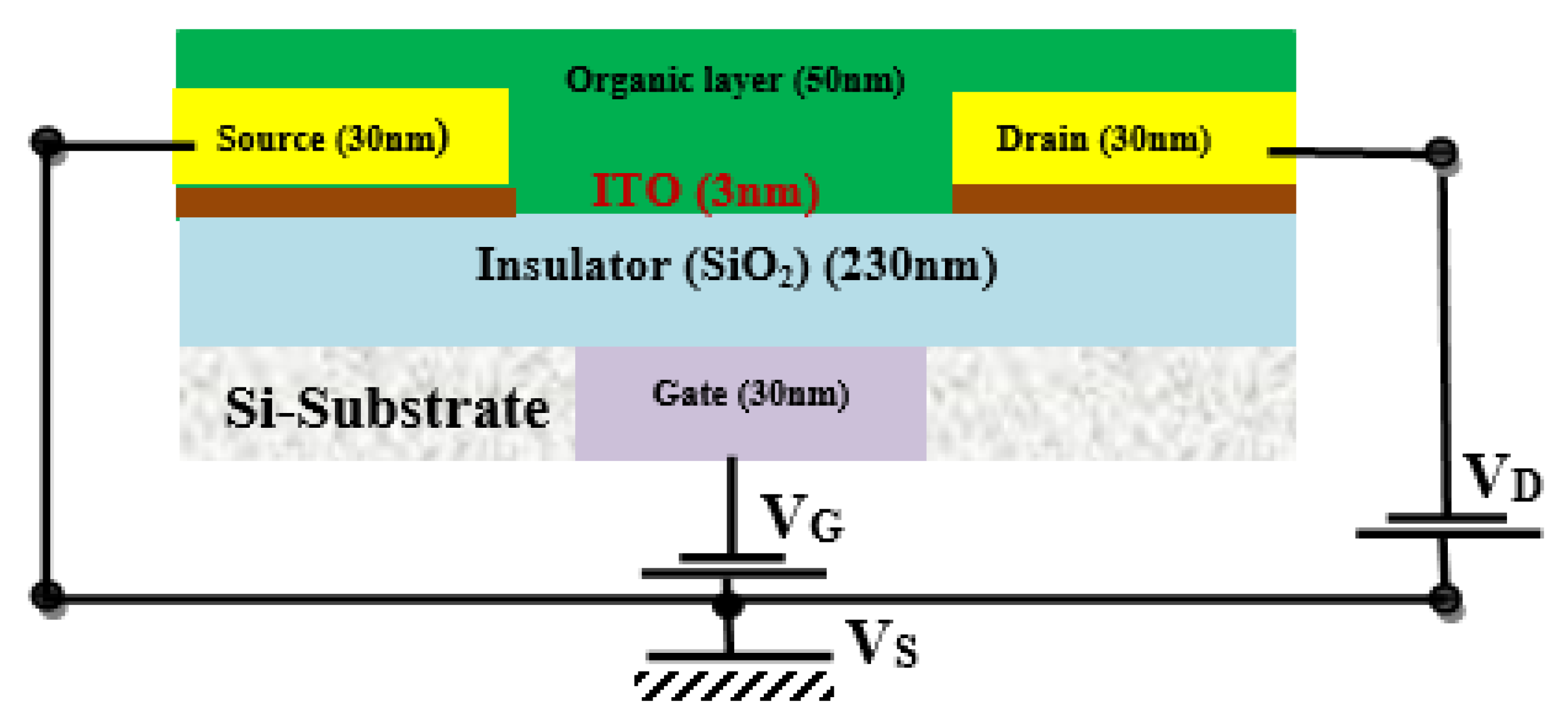
2. Experimental Details

Figure 1 displays a cross-sectional schematic of p-type bottom-contact bottom-gate (BC-BG) organic thin-film transistors (OTFTs) studied in this work. All organic semiconductors were purchased from Aldrich chemical (98% purity) and used without any further purification. The device layers deposited on heavily doped n-type bare silicon (n-Si) served as a substrate and common bottom-gate electrode. All of the substrates were purchased from Fraunhofer Institute for Photonic Microsystems IPMS. Prior to any deposition, these substrates were properly washed under the effect of ultrasonic with acetone, deionized water, and isopropyl alcohol for 10 min each, followed by drying at room temperature with blowing nitrogen gas, and no additional surface treatment was applied. Next, 200 nm of silicon dioxide (is thermally grown, which acts as a gate dielectric for OTFTs. Thirdly, for both metal contacts, i.e., source and drain (S-D), twice-layered of Au (30 nm)/ITO (3 nm) was utilized and patterned via the lift-off technique. Finally, for the active organic layer, 50 nm of organic semiconductors were thermally evaporated with an evaporation rate of 2 Ås−1 and under a high vacuum of 5 × 10⁻⁶ mbar using a preformed mask to complete the structure of the device. Here, OTFTs were fabricated with fixed channel width (W) of 2.0 mm and various channel lengths (L) of 20 μm, 10 μm, 5 μm and 2.5 μm. Electrical measurements of the OTFTs devices were recorded in the dark and vacuum conditions at room temperature using a Keithley Model HP 5156 semiconductor characterization system. The names of the different organic semiconductors and the device abbreviation OTFTs are summarized in Table 1.

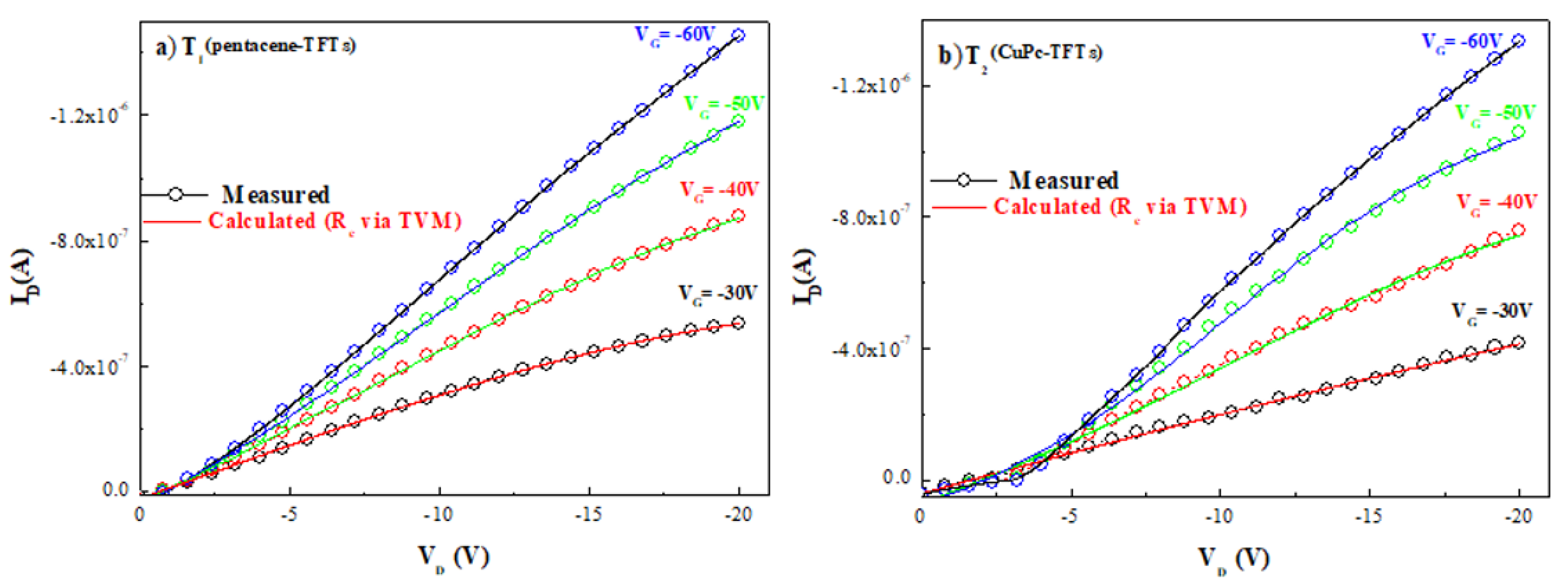
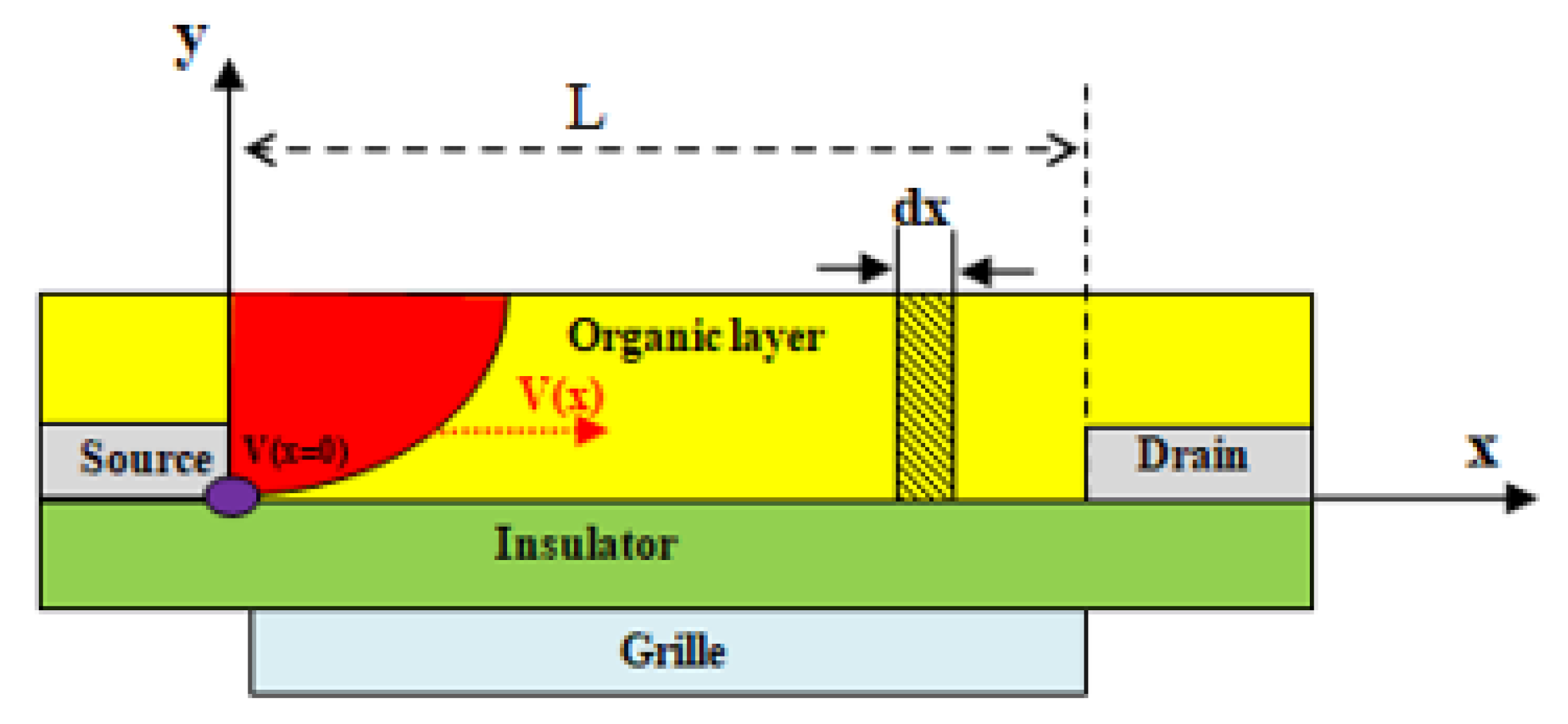
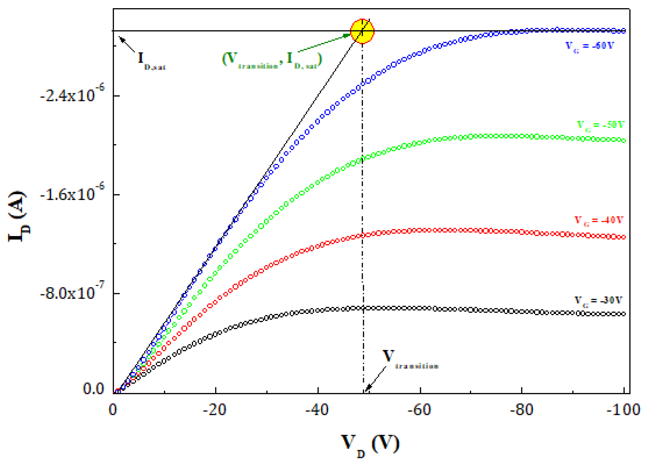
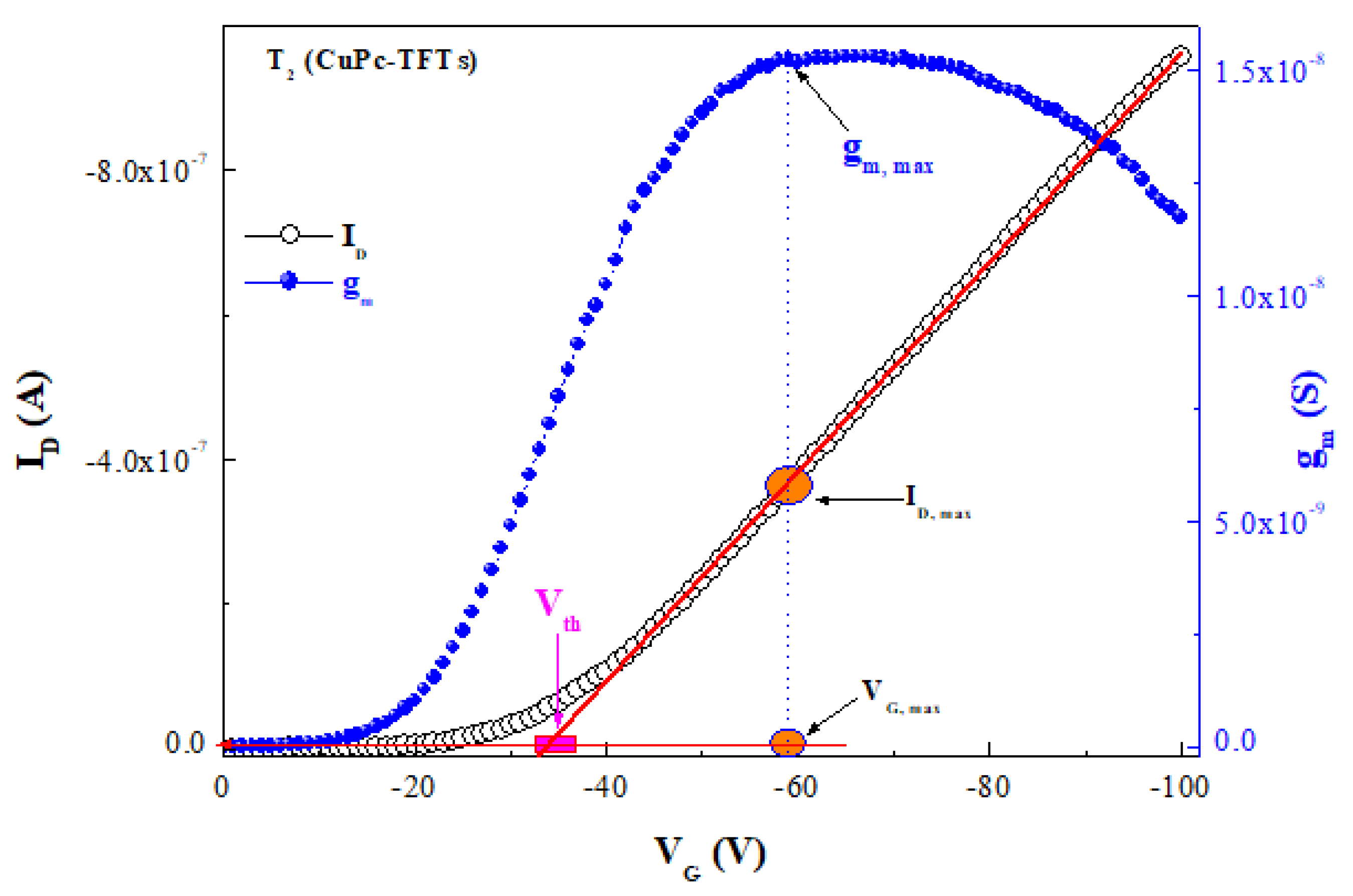
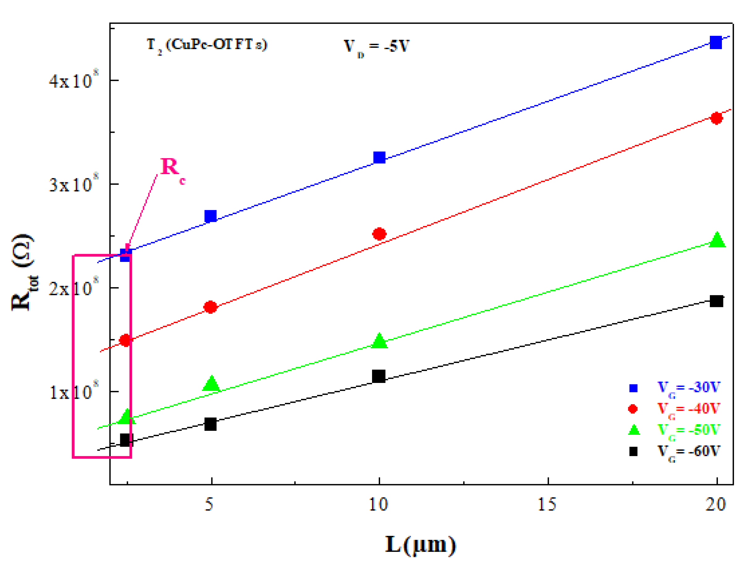
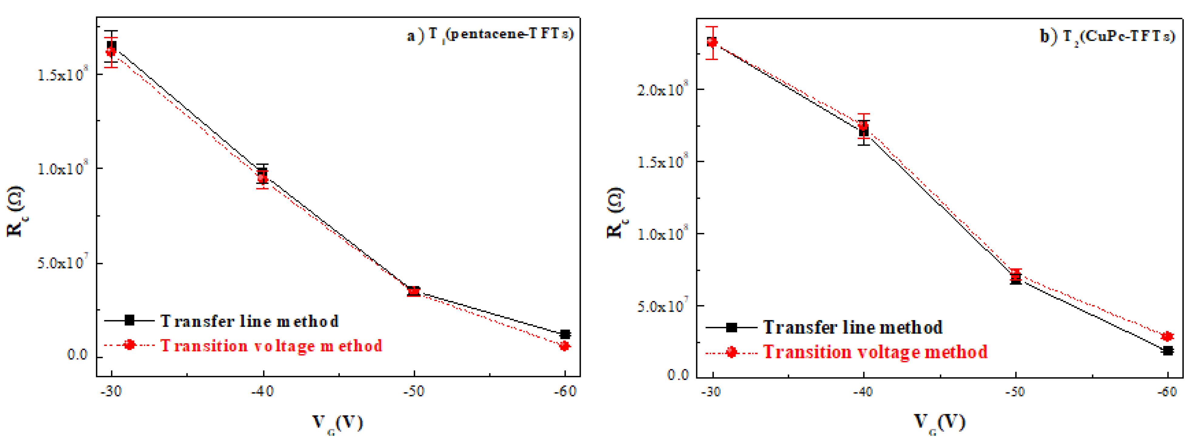
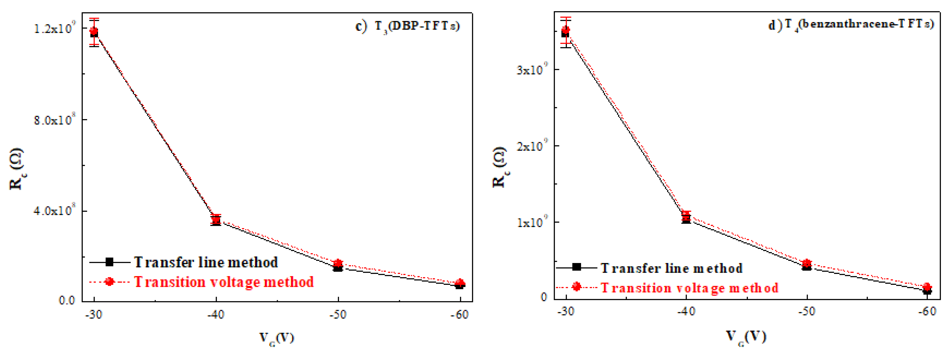
3. Results and Discussion

Contact resistance is one of the important factors that affect the linear region (low drain voltages) of the output characteristics of the OTFTs [26,27,28,29,30,31,32,33,34,35,36,37,38]. This type of resistance acts as a barrier to the injection of charge carriers in OTFTs, thereby influencing their functionality and performance. Consequently, a simple method by which Rc can be simply determined from the OTFTs current-voltage relationships independently of complicated parameters is requested. In this regard, we have developed the transition voltage method (TVM) for extracting Rc. Initially, within the framework of the conventional crystalline semiconductor MOSFETs theory and the graduated channel approximation (i.e., the electrical field along the channel (x-direction) along with the assumption that E x is negligible relative to the electrical field along the y-direction (perpendicular to the channel ( E y E x )), the total drain current ID can be computed by [29,30,31,32,33,39]:
I D = W µ F E C i ( V G V t h V ( x ) ) d V ( x ) d x
where W is the width of channel, Ci is the capacitance per unit area of the insulator, Vth is the threshold voltage, and µFE represents the mobility.
Figure 2 gives the basic geometry definition of the simplified structure of OTFTs used in the calculation of the drain current according to Equation (1). Here, V(x) is the potential with respect to the grounded source electrode at the abscissa x, as shown in Figure 2. Firstly, neglecting Rc and integrating Equation (1) from V(x = 0) = 0 V to V(x = L) = VD leads to the standard-TFTs equations of drain current as a function of VD and VG in both saturation and linear regimes, as follows [29,30,31,32,33,39]:
I D , l i n = W L C i µ F E ( V G V t h V D 2 ) V D
I D , s a t = W 2 L C i µ F E ( V G V t h ) 2
However, the fundamental OTFTs electrical properties may be generally influenced by the existence of the contact resistance (Rc) between the organic active layer/source-drain (S/D) contacts interface. In this regard, we have included the effect of Rc in the definitions of VD and VG. Accordingly, Equations (2) and (3) are modified by accounting for the contact resistance arising from source and drain contacts. For that matter, the integration boundary conditions of Equation (1) become as follow [29,30,31,32,33,39]:
{ V ( x = 0 ) = I D R S V ( x = L ) = V D I D R D
where RS and RD are the series resistances that are satisfying Rc = RS + RD, IDRS and IDRD are voltages that drop through the series resistances RS and RD at the S/D contacts. Taking into account the above conditions, Equation (1) can be integrated from V(x = 0) = IDRS to V(x = L) = VDIDRD to obtain:
I D = W L C i µ F E T [ ( V G V t h ) ( V D I D R D I D R S ) ( V D I D R D ) 2 2 + ( I D R S ) 2 2 ]
At low drain voltage (linear regime), we have the two approximations:
R D = R S = R c 2   and   V G V t h V D
Based on these two approximations, we consequently obtain the simplified equation of ID in the linear regime as follows:
I D , l i n = W L C i µ F E T ( V G V t h ) ( V D 2 I D , l i n R S )
Analogously, at high drain voltage (saturation regime), the pinch-off of the conductive channel from the side of drain electrode occurs at V D I D , s a t R D = V G V t h , so that the ID equation in this regime becomes:
I D , s a t = W 2 L C i µ F E T ( V G V t h I D , s a t R S ) 2
At the transition voltage Vtr between the linear and saturation regimes in the output characteristics, we have VD = Vtr and I D , l i n = I D , s a t , as shown Figure 3, in which the abscissa (VD-axis) is defined as Vtr that verifies Equation (6). Consequently, Equation (6) becomes:
I D , s a t = W L C i µ F E T ( V G V t h ) ( V t r 2 I D , s a t R s )
Finally, we equalize Equation (7) to Equation (8), to derive the analytical expression for the contact resistance as follows [27,33]:
R c = 2 R S = 2 V G V t h [ 2 V t r V G V t h ] I D , s a t
where Vtr and ID,sat are directly determined from the output curve for a given VG. Vtr is the transition voltage, ID,sat is the saturation drain current for a given VG, and Vth is the threshold voltage. Figure 3 shows the graphical method to extract the two parameters Vtr and ID,sat from the intersection of the two slopes in the linear and saturation regimes of the output characteristics. Whereas the linear projection on the y-axis of the intersection of the two slopes of the current-voltage characteristics in the linear and saturation regimes gives the ID,sat value, Vtr corresponds to the linear projection on the x-axis of the intersection of the two slopes. Figure 3 displays some measurements for the device labeled T2 (CuPc-TFTs) as an example for extraction of Vtr and ID,sat.
On the other hand, in the linear regime, the transconductance (gm) has been extracted for each fabricated device using the transfer characteristics ID(VG). In fact, the transconductance (gm) describes the response of the drain current to changes of the gate voltage at a constant drain voltage, which is calculated by the following formula [23]:
g m = [ δ I D δ V G ] V D = c t e = W L µ F E C i V D
Interesting now to Vth extraction in the linear regime, which can be determined using the transfer characteristic and the transconductance curves by means of the extrapolation in the linear region (ELR) method [32]. In this method, adjusting a tangent line to the ID(VG) curve, at the voltage (VG,max) which confronts gm,max, the corresponding value of ID is equivalent to ID,max, the extrapolation of the tangent passing from that point to ID = 0 A is corresponding to the maximum slope of the IDVG curve, that is, the conjunction with I D , m a x = g m , m a x ( V G , m a x V t h ) . This leads to
V t h = I D , m a x g m , m a x + V G , m a x
Figure 4 depicts some measurement for the device T2 (CuPc-TFTs) as an example of the extraction method of Vth by the ELR.
In order to verify the accuracy of TVM, the transfer line method (TLM) was also used to extract the contact resistance of all fabricated OTFTs. In fact, in the frame of the TLM method, the measured total resistance (Rtot) of the device can be modeled as the sum of two series resistances as follows [19,22,23]:
R t o t = R C + R c h ( L ) = R c + L W C i µ F E T , l i n ( V G V t h )
where R c = RS + RD is the resistance associated with the drain and source contacts, R c h is the channel resistance and Rtot is the overall device resistance. Indeed, Rtot was extracted from the linear region of the output characteristics ( R t o t = [ V D I D ] V D 0 V G ) at various high gate voltages (VG = −30 V, −40 V, −50 V and −60 V for various channel lengths (L= 2.5, 5, 10 and 20 µm). In accordance with TLM, Rc is obtained from the intercept with the y-axis by extrapolating the linear fit of the total resistance curve to zero channel length (L = 0 µm).
Figure 5 depicts the computed total resistance for T2 (CuPc-TFTs) device fabricated with different channel lengths as an example.
The obtained values of Rc by the developed TVM (Equation (9)) are compared with those extracted using TLM (Equation (11)) and are shown in Figure 6. Clearly, there is a very good agreement between the two methods in the whole range of gate voltages, with a maximum percentage of difference around 10%. The proposed TVM allows determining the contact resistance as a function of VG, using only one measured output characteristic of a single transistor. All of the foregoing results clearly demonstrate that the proposed TVM is simple, accurate, of general applicability, and a precise alternative method for extracting Rc in OTFTs.
Table 2 recapitulates the main differences in extraction methods of the contact resistance used in this work. Obviously, the extracted values by both methods revealed a decrease of the contact resistance by increasing the gate voltage in all the fabricated OTFTs, as seen in Figure 6. This behavior is mainly due to the supplemental increase of the free carrier density in the conductive channel near the S/D electrodes.
Finally, in order to well confirm the accuracy of TVM, it is worthy to model the output characteristics in the linear regime, by applying the values of contact resistance that we determined using TVM method. To calculate the output characteristics, we have taken in consideration that the value of VG is different from the applied voltage and we denoted by V G . This difference in the value of VG arises because the source contact is not grounded and its potential is increased by the amount that equal RSID, so that [21,22,28,40,41,42,43]:
V G = V G R S I D = V G R C 2 I D
Similarly, the drain voltage VD is considered as V D , as follows [21,22,28,40,41,42,43]:
V D = V D ( R S + R D ) I D = V D R c I D
Injecting Equations (12) and (13) into Equation (2), the drain current in the linear regime takes the following form:
I D = W L C i µ F E T ( V G V t h V D 2 ) V D
Here, in the mobility dependence on the gate, the voltage was also taken into account which can be written as [21,22,28,40,41,42,43]:
µ F E T = µ 0 ( | V G V t h V a a | ) γ
where γ and Vaa are fitting parameters and µ0 is sometimes used as the band mobility for the material of the OTFTs under testing. Replacing Equations (12), (13) and (15) in Equation (14), the drain current expression in the linear regime finally becomes [21,22,28,40,41,42,43]:
I D = ( ( W ( µ 0 V a a γ ) C i ( V G V t h ) γ ) / L { V D ( V G V t h ) ( 1 / 2 ) V D 2 } ) 1 + ( ( W ( µ 0 V a a γ ) C i ( V G V t h ) γ ) / L ) { V D R c / 2 + V D ( V G V t h ) }
The output characteristics in the linear regime of four various types of OTFTs were reproduced using Equation (16) of the drain current that includes the contact resistance in the calculation. The set of parameters that gives a good correspondence between computed values by Equation (16) and those measured are listed in Table 3. The measured output characteristics in the linear regime and those computed by Equation (16), which include the contact resistance values according to the transition voltage method for four different types of OTFTs at different high gate voltages, are compared and shown in Figure 7a–d.
The predicted output characteristics by Equation (16) concurrently with including the mobility dependence on the gate voltage, agree well with the output measurements current-voltage characteristics ID(VD) in the linear regime for various gate voltages (VG = −30 V, −40 V, −50 V and −60 V) for four various types of OTFTs (T1, T2, T3 and T4). Therefore, the model’s ability to describe experimental data and predict the static electrical properties for various types of OTFTs using the contact resistance values according to the transition voltage method confirms the accuracy of TVM. In the light of these results, TVM is an efficient method for contact resistance extracting and can be applied to multiple devices based on different materials.

4. Conclusions

In conclusion, various organic thin-film transistors (OTFTs) made by different organic semiconductors as active layers were fabricated and characterized. A simple and precise transition voltage method (TVM) for Rc extracting was developed and discussed in detail, as well as the obtained values of Rc by the transition voltage method (TVM) were compared to those obtained by the transfer line method (TLM). The obtained Rc values by TVM are in fair agreement with those obtained by TLM with a maximum percentage of difference around 10%, indicating the preciseness of the used transition voltage method. An analytical model was applied to calculate the output characteristics in the linear regime of OTFTs made with various organic semiconductor materials using the contact resistance values obtained by the TVM method. The calculated results in terms of output characteristics in the linear regime are in reasonable agreement with the experimental ones of each fabricated device, which affirms the ability of the used model to describe the charge transport correctly in these types of devices. In the light of these results, TVM only needs single-device characteristics without any complex electrode patterning and can be applied to OTFTs devices produced using various organic structures, generalizing all types of OTFTs. It can be concluded that the used TVM is not only an easy and practical method but also a precise way for extracting Rc in OTFTs and can be applied to various devices produced using different organic materials as an active layer.

Funding

This research received no external funding.

Informed Consent Statement

Not applicable.

Data Availability Statement

All data generated or analyzed during this study are included in this article.

Conflicts of Interest

The authors declare no conflict of interest.

References

  1. Kabe, R.; Adachi, C. Organic long persistent luminescence. Nature 2017, 550, 384–387. [Google Scholar] [CrossRef]
  2. Lia, J.H.; Tang, W.; Wang, Q.; Sun, W.J.; Zhang, Q.; Guo, X.J.; Wang, X.B.; Yan, F. Solution-processable organic and hybrid gate dielectrics for printed electronics. Mater. Sci. Eng. R. Rep. 2018, 127, 1–36. [Google Scholar] [CrossRef]
  3. Geffroy, B.; le Roy, P.; Prat, C. Organic light-emitting diode (OLED) technology: Materials, devices and display technologies. Polym. Int. 2006, 55, 572–582. [Google Scholar] [CrossRef]
  4. Wageh, S. Light Emitting Devices Based on CdSe Nanoparticles Capped with Mercaptoacetic Acid. IEEE J. Quantum Electron. 2014, 50, 741–748. [Google Scholar] [CrossRef]
  5. Eder, F.; Klauk, H.; Halik, M.; Zschieschang, U.; Schmid, G.; Dehm, C. Organic electronics on paper. Appl. Phys. Lett. 2004, 84, 2673–2675. [Google Scholar] [CrossRef]
  6. Wageh, S.; Raïssi, M.; Berthelot, T.; Al-Ghamdi, A.A.; Abusorrah, A.M.; Boukhili, W.; Al-Hartomy, O.A. Silver Nanowires Digital Printing for Inverted Flexible Semi-Transparent Solar Cells. Adv. Eng. Mater. 2021, 23, 2001305. [Google Scholar] [CrossRef]
  7. Alam, M.W.; Wang, Z.; Naka, S.; Okada, H. Performance Enhancement of Top-Contact Pentacene-Based Organic Thin-Film Transistors with Bilayer WO3/Au Electrodes. Jpn. J. Appl. Phys. 2013, 21, 03BB08. [Google Scholar] [CrossRef]
  8. Wageh, S.; Raïssi, M.; Berthelot, T.; Laurent, M.; Rousseau, D.; Abusorrah, A.M.; Al-Hartomy, O.A.; Al-Ghamdi, A.A. Digital printing of a novel electrode for stable flexible organic solar cells with a power conversion efficiency of 8.5%. Sci. Rep. 2021, 11, 14212. [Google Scholar] [CrossRef] [PubMed]
  9. Borchert, J.W.; Peng, B.; Letzkus, F.; Burghartz, J.N.; Chan, P.K.L.; Zojer, K.; Ludwigs, S.; Klauk, H. Small contact resistance and high-frequency operation of flexible low-voltage inverted coplanar organic transistors. Nat. Commun. 2019, 10, 1119. [Google Scholar] [CrossRef] [PubMed] [Green Version]
  10. Hoth, C.N.; Schilinsky, P.; Choulis, S.A.; Brabec, C.J. Printing Highly Efficient Organic Solar Cells. Nano Lett. 2008, 8, 2806–2813. [Google Scholar] [CrossRef] [Green Version]
  11. Alam, M.W.; Wang, S.; Naka, S.; Okada, H. Top Contact Pentacene Based Organic Thin Film Transistor with Bi-layer TiO2Electrodes. J. Photopolym. Sci. Technol. 2012, 26, 659–664. [Google Scholar] [CrossRef] [Green Version]
  12. Kim, K.H.; Kim, K.S.; Ji, Y.J.; Kang, J.E.G.; Yeom, Y. Silicon nitride deposited by laser assisted plasma enhanced chemical vapor deposition for next generation organic electronic device. Appl. Surf. Sci. 2021, 541, 148313. [Google Scholar] [CrossRef]
  13. Kelley, T.W.; Baude, P.F.; Gerlach, C.; Ender, D.E.; Muyres, D.; Haase, M.A.; Vogel, D.E.; Theiss, S.D. Recent Progress in Organic Electronics:  Materials, Devices, and Processes. Chem. Mater. 2004, 16, 4413–4422. [Google Scholar] [CrossRef]
  14. Natali, D. Fundamentals of Organic Electronic Devices, Organic Flexible Electronics Fundamentals, Devices, and Applications Woodhead Publishing Series in Electronic and Optical Materials; Elsevier: Amsterdam, The Netherlands, 2021; pp. 1–25. [Google Scholar]
  15. Borchert, J.W.; Weitz, R.T.; Ludwigs, S.; Klauk, H. A Critical Outlook for the Pursuit of Lower Contact Resistance in Organic Transistors. Adv. Mater. 2021, 35, 2104075. [Google Scholar] [CrossRef] [PubMed]
  16. Hagen, K.; Jackson, T.N. Pentacene organic thin-film transistors and ICs. Solid State Technol. 2000, 43, 63–64. [Google Scholar]
  17. Katz, H.E.; Huang, J. Thin-Film Organic Electronic Devices. Annu. Rev. Mater. Res. 2009, 39, 71–92. [Google Scholar] [CrossRef] [Green Version]
  18. Torsi, L.; Dodabalapur, A.; Sabbatini, L.; Zambonin, P.G. Multi-parameter gas sensors based on organic thin-film-transistors. Sens. Actuators B 2000, 67, 312–316. [Google Scholar] [CrossRef]
  19. Boukhili, W.; Mahdouani, M.; Bourguiga, R.; Puigdollers, J. Experimental study and analytical modeling of the channel length influence on the electrical characteristics of small-molecule thin-film transistors. Superlattices Microstruct. 2015, 83, 224–236. [Google Scholar] [CrossRef] [Green Version]
  20. Boukhili, W.; Mahdouani, M.; Erouel, M.; Puigdollers, J.; Bourguiga, R. Reversibility of humidity effects in pentacene based organic thin-film transistor: Experimental data and electrical modeling. Synth. Met. 2015, 199, 303–309. [Google Scholar] [CrossRef] [Green Version]
  21. Boukhili, W.; Mahdouani, M.; Bourguiga, R.; Puigdollers, J. Temperature dependence of the electrical properties of organic thin-film transistors based on tetraphenyldibenzoperiflanthene deposited at different substrate temperatures: Experiment and modeling. Microelectron. Eng. 2016, 150, 47–56. [Google Scholar] [CrossRef] [Green Version]
  22. Mahdouani, M.; Boukhili, W.; Bourguiga, R. Negative output differential resistance effect in organic thin film transistors based on pentacene: Characterization and modeling Mater. Today Commun. 2017, 13, 367–377. [Google Scholar] [CrossRef]
  23. Boukhili, W.; Mahdouani, M.; Bourguiga, R.; Puigdollers, J. Characterization and modeling of organic thin-film transistors based π-conjugated small molecule tetraphenyldibenzoperiflanthene: Effects of channel length. Microelectron. Eng. 2016, 160, 39–48. [Google Scholar] [CrossRef] [Green Version]
  24. Boukhili, W.; Tozlu, C.; Mahdouani, M.; Erten-Ela, S.; Bourguiga, R. Illumination and dipole layer effects on the density of state distribution in n-type organic thin film phototransistors based on naphthalene bis-benzimidazole: Experiment and modeling. Microelectron. Eng. 2017, 179, 37–47. [Google Scholar] [CrossRef]
  25. Fan, C.L.; Lin, Y.Z.; Lee, W.D.; Wang, S.J.; Huang, C.H. Improved pentacene growth continuity for enhancing the performance of pentacene-based organic thin-film transistors. Org. Electron. 2012, 13, 2924–2928. [Google Scholar] [CrossRef]
  26. Marinkovic, M.; Belaineh, D.; Wagner, V.; Knipp, D. On the origin of contact resistances of organic thin film transistors. Adv. Mater. 2012, 24, 4005. [Google Scholar] [CrossRef]
  27. Natali, D.; Caironi, M. Charge Injection in Solution-Processed Organic Field-Effect Transistors: Physics, Models and Characterization Methods. Adv. Mater. 2012, 24, 1357–1387. [Google Scholar] [CrossRef] [PubMed]
  28. Al-Ghamdi, A.; Boukhili, W.; Wageh, S. Contact resistance corrected-electrical characteristics with channel length effects in π-conjugated small-molecule benzanthracene organic thin film transistors. Synth. Met. 2021, 273, 116670. [Google Scholar] [CrossRef]
  29. Natali, D.; Fumagalli, L.; Sampietro, M. Modeling of organic thin film transistors: Effect of contact resistances. J. Appl. Phys. 2007, 101, 014501. [Google Scholar] [CrossRef]
  30. Neamen, D.A. Semiconductor Physics and Devices: Basic Principles, 4th ed.; McGraw-Hill: New York, NY, USA, 2012. [Google Scholar]
  31. Pesavento, P.V.; Chesterfield, R.J.; Newman, C.R.; Frisbie, C.D. Gated four-probe measurements on pentacene thin-film transistors: Contact resistance as a function of gate voltage and temperature. J. Appl. Phys. 2004, 96, 7312. [Google Scholar] [CrossRef]
  32. Schroder, D.K. Semiconductor Material and Device Characterization, 3rd ed.; John Wiley & Sons, Inc.: Hoboken, NJ, USA, 2006. [Google Scholar]
  33. Wang, S.D.; Yan, Y.; Tsukagoshi, K. Transition-Voltage Method for Estimating Contact Resistance in Organic Thin-Film Transistors. IEEE Electron. Device Lett. 2010, 31, 509–511. [Google Scholar] [CrossRef]
  34. Jinhuo, C.; Jiaxing, H.; Yunlong, Z. A novel method to analyze the contact resistance effect on OTFTs. J. Semicond. 2012, 33, 124005. [Google Scholar]
  35. Lai, S.; Cosseddu, P.; Bonfiglio, A. A method for direct contact resistance evaluation in low voltage coplanar organic field-effect transistors. Appl. Phys. Lett. 2017, 110, 153304. [Google Scholar] [CrossRef]
  36. Takagaki, S.; Yamada, H.; Noda, K. Extraction of contact resistance and channel parameters from the electrical characteristics of a single bottom-gate/top-contact organic transistor. Jpn. J. Appl. Phys. 2016, 55, 03DC07. [Google Scholar] [CrossRef]
  37. Torricelli, F.; Ghittorelli, M.; Colalongo, L.; Kovacs-Vajna, Z.M. Single-transistor method for the extraction of the contact and channel resistances in organic field-effect transistors. Appl. Phys. Lett. 2014, 104, 093303. [Google Scholar] [CrossRef] [Green Version]
  38. Necliudov, P.V.; Shur, M.S.; Gundlach, D.J.; Jackson, T.N. Contact resistance extraction in pentacene thin film transistors. Solid-State Electron. 2003, 47, 259–262. [Google Scholar] [CrossRef]
  39. Horowitz, G.; Hajlaoui, R.; Fichou, D.; el Kassmi, A. Gate voltage dependent mobility of oligothiophene field-effect transistors. J. Appl. Phys. 1999, 85, 6. [Google Scholar] [CrossRef]
  40. Simonetti, O.; Giraudet, L.; Maurel, T.; Nicolas, J.L.; Belkhir, A. Organic transistor model with nonlinear injection: Effects of uneven source contact on apparent mobility and threshold voltage. Org. Electron. 2010, 11, 1381–1393. [Google Scholar] [CrossRef]
  41. Bolognesi, A.; Berliocchi, M.; Manenti, M.; Carlo, A.D.; Lugli, P.; Lmimouni, K.; Dufour, C. Effects of grain boundaries, field-dependent mobility, and interface trap States on the electrical Characteristics of pentacene TFT. IEEE Trans. Electron. Devices 2004, 51, 1997. [Google Scholar] [CrossRef]
  42. Haddock, J.N.; Zhang, X.; Zheng, S.; Zhang, Q.; Marder, S.R.; Kippelen, B. A comprehensive study of short channel effects in organic field-effect transistors. Org. Electron. 2006, 7, 45–54. [Google Scholar] [CrossRef]
  43. Jung, K.D.; Kim, Y.C.; Park, B.G.; Shin, H.; Lee, J.D. Modeling and parameter extraction for the series resistance in thin-film transistors. IEEE Trans. Electron. Devices 2009, 56, 431–440. [Google Scholar] [CrossRef]
Figure 1. A schematic view of the bottom-gate bottom-contact organic thin-film transistors used in this experiment with its polarization condition.
Crystals 11 01448 g001
Figure 2. Geometry definition of a simplified structure of OTFTs used in the calculation of the drain current expression (Equation (1)) in the frame of the graduated channel approximation ( E y E x ).
Crystals 11 01448 g002
Figure 3. Graphical method extraction of the parameters Vtransition and ID,sat from the intersection of the two slopes in the linear and saturation regimes of the output characteristics (an example for ID-VD of T2 (CuPc-TFTs) at high gate voltages).
Crystals 11 01448 g003
Figure 4. Illustration of the process of extraction of the Vth by the linear extrapolation method from transfer characteristics IDVG (left axis) and transconductance gm (right axis) as a function of VG in the linear regime (an example of measurement for T2 (CuPc-TFTs)).
Crystals 11 01448 g004
Figure 5. Total resistance as a function of channel length of the T2 (CuPc-TFTs) for different high negative gate voltages. Illustration of the process of extraction of the Rc using TLM.
Crystals 11 01448 g005
Figure 6. Comparison of the obtained values by the transition voltage method (circle) and the transfer line method (full square) of the contact resistance as a function of the VG of all fabricated OTFTs in linear regime: (a) for T1 (pentacene-TFTs), (b) for T2 (CuPc-TFTs), (c) for T3 (DBP-TFTs) and (d) for T4 (benzanthracene-TFTs).
Crystals 11 01448 g006aCrystals 11 01448 g006b
Figure 7. Comparison of the measured (circle) output characteristic curves in the linear regime and the calculated data including the extracted contact resistance using the transition voltage method of OTFTs based on various organic materials: (a) T1 (pentacene-TFTs), (b) T2 (CuPc-TFTs), (c) T3 (DBP-TFTs) and (d) T4 (benzanthracene-TFTs).
Crystals 11 01448 g007aCrystals 11 01448 g007b
Table 1. Organic semiconductors that were applied as an active layer and the device abbreviation names.
Organic SemiconductorsDevice Abbreviation Name
PentaceneT1 (Pentacene-TFTs)
Copper phthalocyanine (CuPc)T2 (CuPc-TFTs)
Tetraphenyldibenzoperiflanthene (DBP)T3 (DBP-TFTs)
BenzanthraceneT4 (Benzanthracene-TFTs)
Table 2. Comparison summary of extraction methods of the contact resistance used in this work.
Method NameAbbreviationNumber
of Transistor
Required
Parameters
Required
Measurement
Transfer line methodTLMset of transistors: various channel lengthsTotal resistance
Mobility
Threshold voltage
ID-VD of multiple OTFTs
Transition voltage methodTVMSingle transistorThreshold voltageID-VD of single OTFTs
Table 3. Fitting parameters that give a fair agreement between the measured output characteristics in the linear regime and those calculated by Equation (15).
Parameters DeviceVaa (V)γ µ 0 ( cm 2   V 1   s 1 ) Vth (V)
T11.221.117.7 × 10–6−36
T20.981.852.6 × 10–6−37.75
T31.741.297.8 × 10–7−42.5
T41.351.032.73 × 10–7−45.61
Publisher’s Note: MDPI stays neutral with regard to jurisdictional claims in published maps and institutional affiliations.

