Article

Thermodynamic Study of Adsorption Capacity between Metal Film and Optical Crystal: Adsorption Energy of Ni Films on LiNbO3 Substrates

1
School of Information Science and Engineering, Shandong University, Qingdao 266237, China
2
Department of Radiation Oncology, Qilu Hospital of Shandong University, Jinan 250012, China
*
Author to whom correspondence should be addressed.
Crystals 2021, 11(11), 1273; https://doi.org/10.3390/cryst11111273
Submission received: 17 September 2021 / Revised: 15 October 2021 / Accepted: 16 October 2021 / Published: 20 October 2021
(This article belongs to the Special Issue Ferroelectric and Piezoelectric Crystals)

Abstract

:
The growth of large areas of two-dimensional homogeneous graphene depends on the bond between the metal film, which acts as a catalyst, and the substrate material. The structural differences between the metal and the various anisotropic crystals make this growth method a challenge for the feasibility of growing graphene on optical crystals. In this paper, the evolution of the adsorption energy between nickel (Ni) films and Lithium Niobate (LiNbO3, LN) crystals is modelled under different thermal treatment environments by constructing a physical model of the temperature dependence of the adsorption energy between the two materials. With the aid of a series of simulated full annealing processes, the changes in adsorption energy at different temperatures were calculated. The results show that there are two “temperature windows” with target annealing temperatures of 700–800 K and 950–1050 K that prove to have high adsorption energies. This is of great guiding and practical significance for the direct transfer-free synthesis of graphene on LiNbO3 substrates.

1. Introduction

Since graphene was first prepared by mechanical exfoliation in 2004 [1], research reports on graphene have sprung up due to its fascinating physical and electrical properties, such as excellent mechanical strength [2], ultrafast carrier mobility [3], near transparency in a wide spectral range from visible to infrared [4], and high thermal conductivity [5]. One of the most important parts is the direct synthesis of graphene on the desired substrate [6,7,8], as this transfer-free method avoids the additional graphene degradation introduced by the wet-transfer process and is conducive to the performance of the device.
The most reported desired substrate is insulating SiO2/Si substrate [8,9,10,11,12,13,14,15,16], because a graphene layer on an insulating SiO2/Si substrate is an important structural arrangement used in the fabrication of graphene-based electrical devices. For transfer-free direct growing of graphene films on SiO2/Si substrate, the method commonly used by researchers is chemical vapor deposition (CVD) [7,8,15]. The typical process is as follows: Under the assistance of plasma and high temperature, the carbon precursor (such as methane gas (CH4)) was decomposed, and the dissociated carbon atoms were in contact with the surface of the catalytic metal, Ni, deposited on SiO2/Si. At high temperature, a large number of carbon atoms could dissolve into the metal Ni and distribute throughout the solid metal; then, as the temperature gradually decreases, the supersaturated carbon atom would precipitate and associate to form graphene layers both on the top of Ni and at the interface between Ni and SiO2/Si substrate due to the reduced solubility of carbon in Ni. Finally, the graphene-SiO2/Si structure was obtained after the metal film was etched away. There are also a few reports of direct synthesis of graphene films by ion implantation on insulating substrates of SiO2/Si. R. Zhang et al. reported transfer-free synthesis of graphene layers on SiO2/Si substrates by ion implantation at room temperature [6]. Negatively charged carbon atoms with certain energy and dose were implanted into Ni film capped on SiO2/Si; afterwards, ex-situ annealing treatment was conducted. The implanted carbon atoms first underwent dissolution and diffusion in the Ni film at an elevated temperature, and then they subsequently precipitated and aggregated on both sides of the Ni film during the cooling stage. Next, the Ni thin film, together with the upper layer graphene formed on the top of it, was removed, and the graphene-SiO2/Si structure was obtained.
For both the CVD and the ion implantation methods, the growth of graphene undergoes a similar process: the carbon solubility in Ni is reduced by lowering the temperature, which makes the carbon precipitated from the carbon-doped metal Ni form graphene. The difference between the two methods is the way of carbon doping: for the CVD method, carbon atoms are introduced into Ni films by the decomposition of carbonaceous precursor at high temperatures on the Ni surface; for the ion implantation method, doping of Ni films with carbon atoms is achieved by direct implantation of carbon. The flexibility of direct implantation allows the concentration and distribution of doped carbon atoms in the Ni film to be adjusted at will. However, the non-thermal equilibrium process of implantation also complicates the physical process of carbon precipitation.
In recent years, much of the research on graphene is focused on graphene-SiO2/Si structure, whether it is the synthesis of graphene (mentioned above) or the application of graphene-component optoelectronic devices (such as high-speed transistors [17,18,19], high-sensitivity sensors [20,21,22], and high-performance solar cells [23,24,25]). Few studies have addressed the structural properties between graphene and non-Si substrates. One of the most interesting topics reported in these investigations is the study of the structure between graphene and the “all-purpose” optical crystal LiNbO3. LiNbO3 is a promising material in fundamental and applied sciences [26,27,28], which has ferroelectric, photovoltaic, piezoelectric, pyroelectric, photo-elastic, and photorefractive properties [29]. The graphene attached to LiNbO3 is likely to be influenced by the properties of the crystal, which in turn allows the quantum effects of its two-dimensional material to be modulated. For example, some studies have theoretically explored the interfacial properties of the combination of graphene and LiNbO3 crystals [30,31]. One typical example is the modulation of carrier doping of graphene via LiNbO3 polarization properties. The results show that, by adjusting the carrier doping of graphene in the graphene/LiNbO3 structure, the excitation and propagation of surface plasmon polaritons can be controlled.
Direct synthesis of graphene on LiNbO3 has not been reported except by our research group [32,33]. In 2020, we reported the direct synthesis of graphene on the surface of LiNbO3 by annealing a post-carbon-implantation sample consisting of surface metal Ni film and LiNbO3 substrate [33]. The transfer-free synthesis of graphene on LiNbO3 substrate avoids the additional graphene degradation and, more importantly, substrate combined with a patterned metal film suggests the possibility of engineering two-dimensional graphene with special confinement, which is often emphasized in photoelectric crystals such as LiNbO3. Unfortunately, in the first attempt, the graphene formed on LiNbO3 is unevenly distributed and contains a variety of structures, such as multilayer or turbostratic graphene and even amorphous carbon [33]. There may be multiple reasons for this result; however, the extremely poor distribution of the Ni film deposited on the LiNbO3 surface is the most direct cause of this result. For example, the detachment of the Ni film from the LiNbO3 substrate during the heat treatment can lead to local aggregation of precipitated carbon. The macroscopic result of this detachment is that the Ni film wrinkles after suffering annealing treatment. The occurrence of this phenomenon seems to be related only to the nature of the two materials (the Ni film and the LiNbO3 substrate) themselves, and not to the process of carbon doping, because two kinds of samples (one without carbon ion implantation and the other with carbon ion implantation) with the same coating treatment were found to have similar wrinkles after the same annealing process. As shown in Figure 1, the wrinkles that appeared on the sample treated with ion implantation are slightly larger than those on the sample without ion implantation. This can be attributed to the ion implantation and the movement of carbon to the interface during annealing, which weakens the adsorption force between LiNbO3 and Ni, so it is not difficult to deduce that the formation of wrinkles is a direct consequence of the poor adhesion of Ni film on LiNbO3 substrate. Improving the adhesion between the Ni film and the LiNbO3 substrate is one of the key factors for ensuring the uniformity of carbon distribution.
Therefore, it is particularly important to find the suitable annealing temperature range that maximizes the adsorption energy between Ni film and LiNbO3 substrate to ensure that their interface is always homogeneous during the graphene precipitation. This is advantageous for both CVD and ion implantation methods, because both methods require high temperature heat treatment of the sample to obtain graphene.
In this article, a model of LiNbO3 substrate covered with Ni film was built, and the adsorption energies between LiNbO3 substrate and Ni film were calculated by a molecular dynamics simulation with full annealing process at different target (peak) temperatures. The “temperature window” with the best (maximum) adsorption energy was found for the combination of Ni film and LiNbO3 substrate. Within the “temperature window”, the adsorption energy of the two materials is relatively large, which makes the Ni film less likely to detach from the LiNbO3 substrate during the annealing process, thus creating conditions for the precipitated carbon atoms to form a uniform graphene structure.

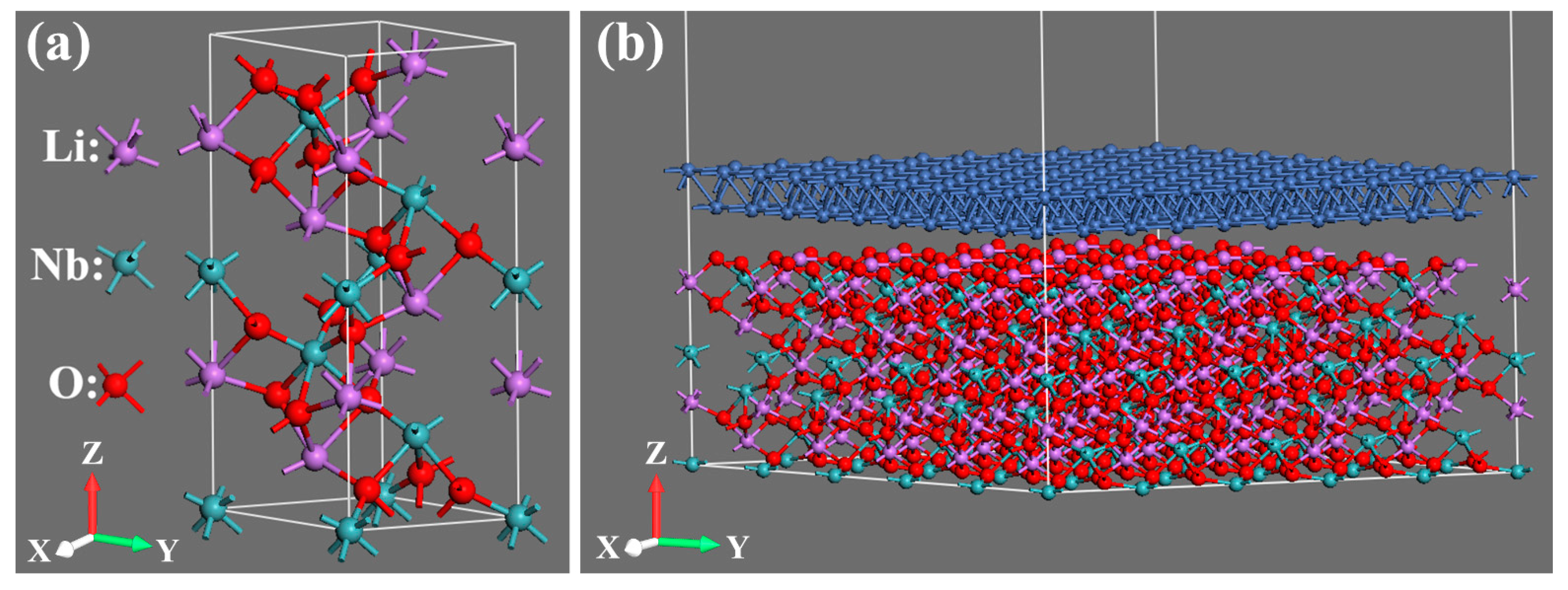
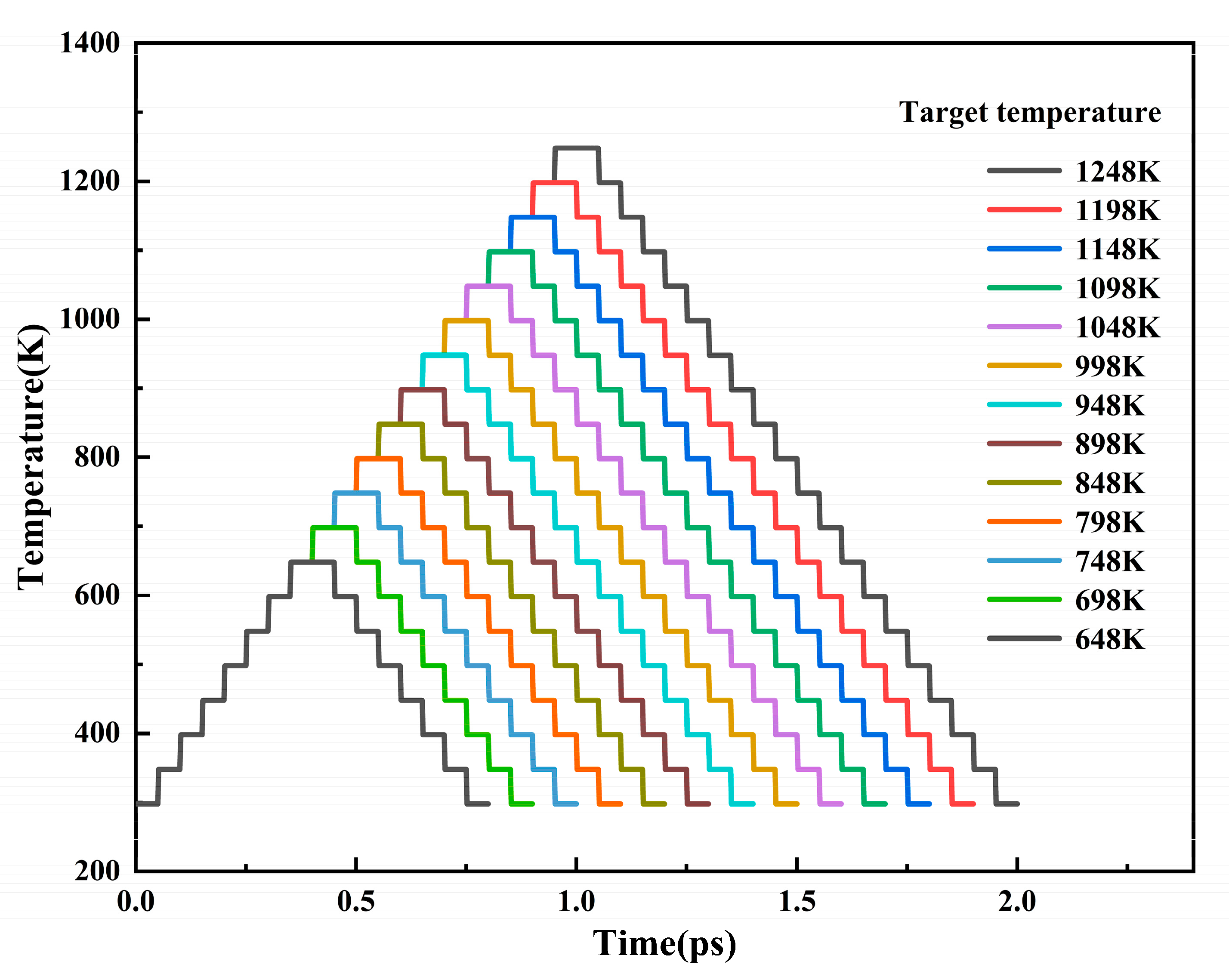
2. Model Building and Simulation Method

LiNbO3 (PDF#: 20-0631) crystal is a ferroelectric crystal that belongs to the R3c space group at temperatures below 1210 °C. When represented by a hexagonal coordinate system, the lattice parameters of LiNbO3 crystal measured by experiments are a = b = 5.1516 Å, c = 13.869 Å, α = β = 90°, γ = 120° [34], and the coordinates of the atoms are shown in Table 1. A LiNbO3 unit cell was built with the above parameters, and then the geometry optimization of the LiNbO3 unit cell was performed using the ultrasoft pseudopotential of the plane-wave, to obtain a more stable crystal structure. The optimized LiNbO3 unit cell is shown in Figure 2a, which contains 6 Lithium (Li) atoms, 6 Niobium (Nb) atoms, and 18 Oxygen (O) atoms. The optimized lattice parameters are extremely close to the experimental values, as revealed by Table 2. The model of LiNbO3 substrate covered with Ni (PDF#: 04-0850) film is present in Figure 2b; the underlying LiNbO3 consists of a 5 × 5 expanded cell of (001) LiNbO3, which contains 150 Lithium (Li) atoms, 150 Niobium (Nb) atoms, and 450 Oxygen (O) atoms. The upper layer is the (111) Ni layer, which contains 200 atoms and a vacuum layer of 50 Å, was added on top of the Ni film to isolate the influence of other cells in the Z direction. The final super cell was 25.4025 Å × 25.4025 Å × 68.7595 Å. The LiNbO3 (001) was chosen for the study because, in our previous experiments, Ni film exfoliation occurred in Ni-deposited LiNbO3 (001) samples. We also chose an Ni (111) surface for simulation for two reasons: one is that Ni (111) has the greatest chance (77.6%) of becoming a surface through the calculation of Materials Studio software’s morphology tools, while the other is that when Ni film is laminated with LiNbO3, only the Ni (111) surface produces the least deformation so it is easier to form a stable structure between them.
The annealing process was simulated based on the molecular dynamics method. The universal force field model is used here because it can be applied to all elements in the periodic table and thus can be used to describe the new combination of Ni and LiNbO3 structures [35]. During the annealing simulation, we used a canonical ensemble (NVT) for the system while the velocity scale was adopted for temperature control. A total of 13 groups of annealing processes were simulated. During each full round of the annealing process, the temperature was increased from room temperature at 298 K to the target annealing temperature and then decreased to 298 K. The parameters of all the annealing process are shown schematically in Figure 3. The horizontal axis of the graph indicates the required time to raise or lower the temperature, and the overall parallel distribution represents the consistent rate of raising and lowering the temperature during each round of annealing. This means that an increase in the target temperature represents an increase in the time to raise or lower the temperature. For example, the heating ramps were set to 20 steps when the target annealing temperature was 1248 K and 19 steps when the target annealing temperature was 1198 K.
The adsorption energies between metal Ni film and LiNbO3 substrate at different temperatures were calculated as E = | E L N + N i E L N E N i | [36,37]. Here, E L N + N i is the energy corresponding to the system formed by the LiNbO3 substrate and Ni film; E L N is the energy of the isolated LiNbO3 substrate; and E N i is the energy of the Ni film alone.

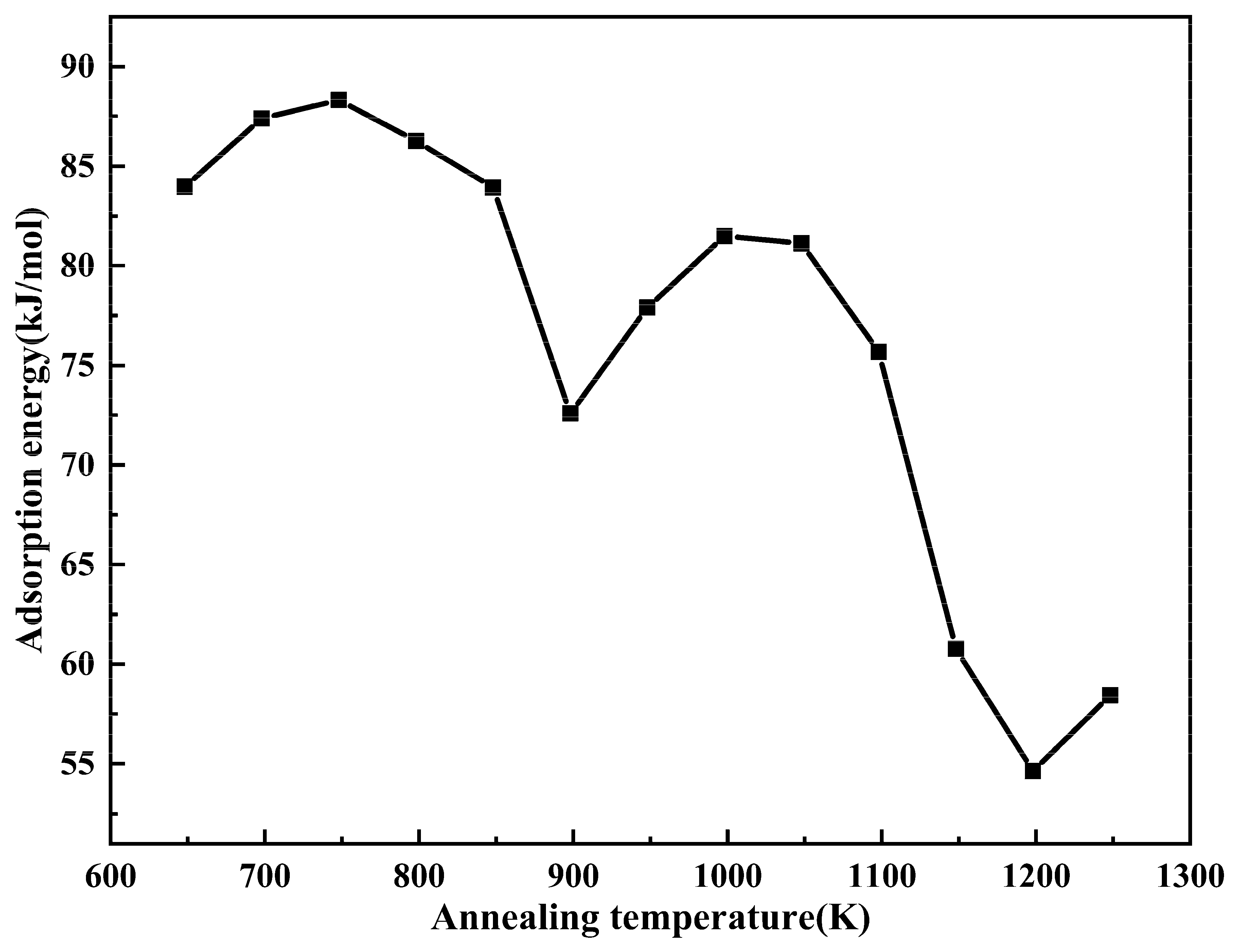
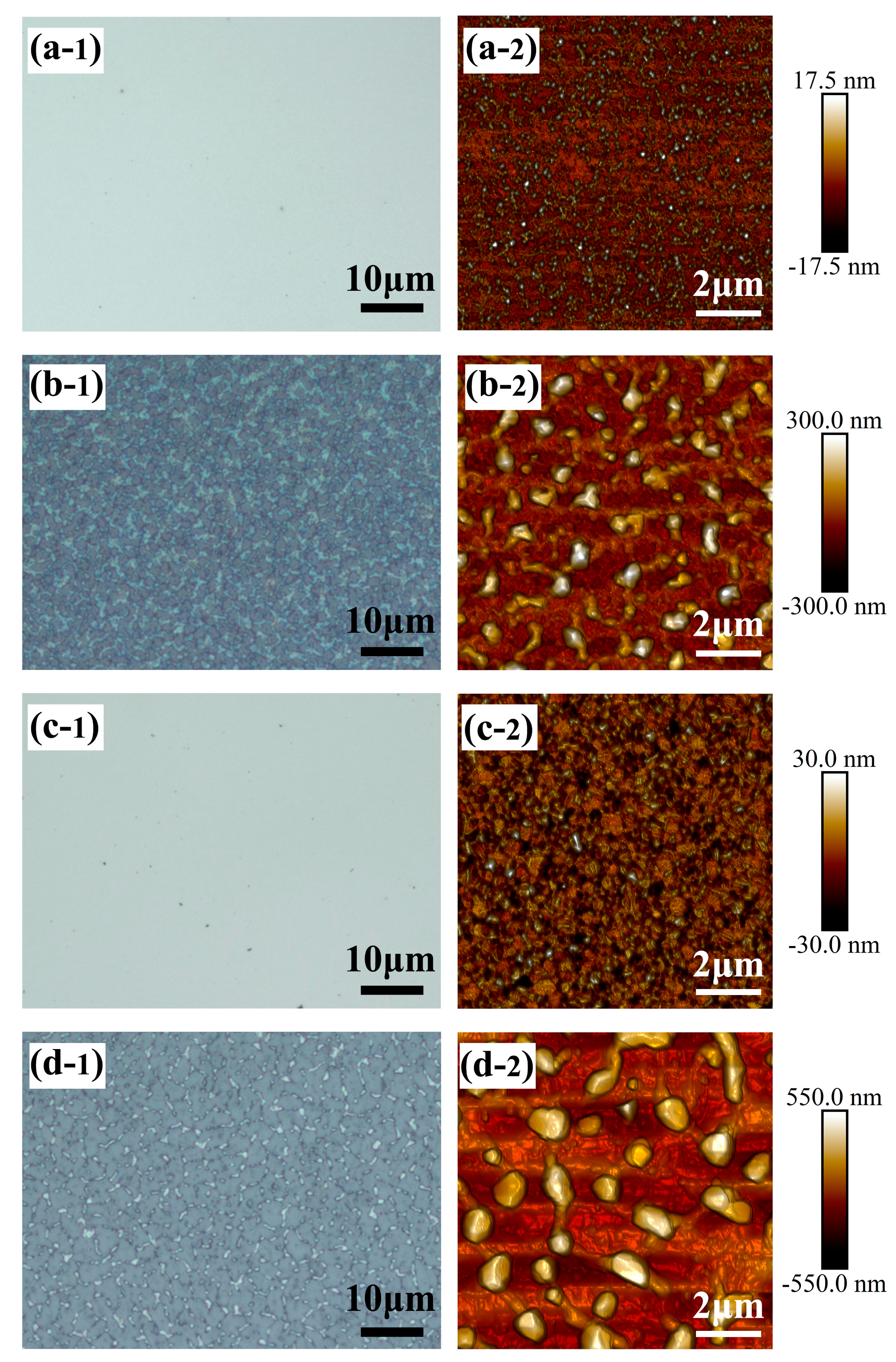
3. Results and Discussion

The change curve of adsorption energy at different target annealing temperatures is shown in Figure 4, where the calculated adsorption energy at each point corresponds to the value at the completion of an annealing process. In general, the adsorption energy between Ni and LiNbO3 decreases with the increase in the target annealing temperature because the higher the temperature is, the more active the particles are. When the temperature is high enough, the Ni film has enough driving energy to detach from the adsorption of LiNbO3 substrate. Once this happens, it means that the original adsorption force cannot be recovered even if the atoms undergo a further cooling process. However, after simulating the complete annealing process for each round, the calculations show that, with a change in target temperature from 648 K to 1248 K, the combined structure of Ni and LiNbO3 does have two “temperature windows” at 700–800 K and 950–1050 K, which correspond to the maximum value of the adsorption energy. This means that the adsorption energy of Ni and LiNbO3 can reach the maximum when the target annealing temperature lies in either of these two “temperature windows”. Among the two “temperature windows”, although the lower “temperature window” 700–800 K corresponds to a higher adsorption energy, considering that the temperature required for carbon diffusion and precipitation in Ni films is usually higher than 900 K, a more feasible annealing “temperature window” for practical applications should be at 950–1050 K.
To explain the existence of “temperature windows” in the annealing process, we calculated the variations in adsorption energy during cooling process in each group of annealing at different target temperatures. Figure 5 is the three-dimensional mapping diagram of adsorption energy during the cooling process. It can be clearly seen that there are two extreme values of adsorption energy in the considered range of annealing parameters. In these two regions, where the adsorption energy is extremely high, take any two points and make the curve of the adsorption energy with a cooling temperature; the results are shown in Figure 6a,b. The trend of these two curves shows that the adsorption energy of Ni and LiNbO3 increases almost monotonically as the annealing temperature decreases. Beyond these two regions, the adsorption energy of Ni and LiNbO3 hardly changes with the temperature throughout the cooling process, except for small rises and falls, as shown in Figure 6c,d. It seems that, in the process of cooling, two modes exist for adsorption energy variation with temperature for the combination of Ni and LiNbO3. Only in the mode of increasing adsorption energy with temperature is it possible to maintain a high adsorption energy between Ni and LiNbO3 after a round of the annealing process. Therefore, to maintain the stability of Ni films during graphene growth, setting the target temperature of annealing within these two “temperature windows” is essential to form uniform graphene on LiNbO3 optical crystal substrates.
It is worth noting that the results of the simulations show that the adsorption energy does not decrease monotonically as the target temperature increases, as would usually be expected; instead, there are maximum values of adsorption energy in the two temperature regions, as shown in Figure 4. It seems that the temperature-dependent atomic driving forces may have specific optimal values when equilibrating the adsorption energy. However, in our simulations, the calculation of the adsorption energy is based on the consideration of many contributions from multiple parameters, the physical mechanism of which will be studied further.
To verify our simulation results, four nickel-plated LiNbO3 samples were annealed at the same annealing condition with different target temperatures; the surface morphologies after treatment are shown in Figure 7. The target annealing temperatures used in Figure 7a,c lie exactly in the range of two “temperature windows”, 700–800 K and 950–1050 K, respectively, which have high adsorption energies between LiNbO3 substrate and Ni film according to our simulation. As can be seen from the optical microscope images of Figure 7a,c, the surfaces of the two samples are relatively flat and the results using an atomic force microscope (AFM) are also consistent with those of an optical microscope; however, several large grains can be found in Figure 7c-2, which are generated under higher temperature heat treatment. For the samples with a target annealing temperature outside the “temperature window”, the surface morphology of the samples has a completely different appearance, which is shown in Figure 7b,d. Some fold-like morphologies appear on the surface. From our perspective, after suffering high heat temperature treatment, the Ni film detached at some positions from the LiNbO3 surface because of the weak adsorption energy and bulged upward, while some of the Ni atoms moved into the space below the bulges to form clusters. This aggregation of Ni atoms is more likely to intensify at high temperatures, so the Ni particles in Figure 7d are significantly larger than those in Figure 7b. Our current experimental results give good support to the simulation results of the Ni and LiNbO3 combined structure. It also provides an important reference for the direct growth of two-dimensional graphene structures on anisotropic crystalline materials using the catalytic effect of metal thin films.

4. Conclusions

We built a model of LiNbO3 substrate covered with Ni film and systematically simulated the changes in adsorption energy between them at different temperatures. The adsorption energy after the complete annealing process (heating to the target annealing temperature and then cooling to room temperature) was calculated for different target annealing temperatures from 648 K to 1248 K. Two “temperature windows”, with the target annealing temperatures of 700–800 K and 950–1050 K, were found and proved to have high adsorption energies by both simulation and experiment. The results of the simulated cooling process show that the adsorption energy rises with a decreasing temperature for annealing processes when the target temperature is exactly in the “temperature window”, which indicates a better adsorption between the Ni film and the surface of LiNbO3 substrate. Outside the “temperature window”, the adsorption energy only fluctuates at a lower level and is largely independent of the actual annealing temperature. This indicates that, when the target temperature lies in the “temperature window”, strong adsorption energy between the Ni film and the LiNbO3 makes it difficult to detach the Ni film from the LiNbO3 substrate, thereby creating conditions for the growth of a uniform large-area graphene film with high quality. This is of great guiding and practical significance for the direct transfer-free synthesis of graphene on LiNbO3 or other substrates.

Author Contributions

Conceptualization, Y.X. and F.L.; data curation, Y.X.; formal analysis, Y.X. and F.L.; funding acquisition, F.L.; investigation, Y.X., K.L. and C.M.; methodology, Y.X. and F.L.; project administration, Y.X. and F.L.; resources, F.L.; software, Y.X. and F.L.; supervision, F.L.; validation, F.L.; visualization, Y.X.; writing—original draft, Y.X.; writing—review and editing, Y.X. and F.L. All authors have read and agreed to the published version of the manuscript.

Funding

This research was funded by the National Natural Science Foundation of China, grant number 61975094, and the National Natural Science Foundation of China, grant number 12005119.

Data Availability Statement

The data presented in this study are available on request from the corresponding author.

Conflicts of Interest

The authors declare no conflict of interest.

References

  1. Novoselov, K.S.; Geim, A.K.; Morozov, S.V.; Jiang, D.; Zhang, Y.; Dubonos, S.V.; Grigorieva, I.V.; Firsov, A.A. Electric field effect in atomically thin carbon films. Science 2004, 306, 666–669. [Google Scholar] [CrossRef] [Green Version]
  2. Lee, C.; Wei, X.; Kysar, J.W.; Hone, J. Measurement of the elastic properties and intrinsic strength of monolayer graphene. Science 2008, 321, 385–388. [Google Scholar] [CrossRef] [PubMed]
  3. Chen, C. Surface Chemistry and Macroscopic Assembly of Graphene for Application in Energy Storage. Ph.D. Thesis, University of Chinese Academy of Sciences, Beijing, China, 2015. [Google Scholar]
  4. Zhu, Y.; Murali, S.; Cai, W.; Li, X.; Suk, J.W.; Potts, J.R.; Ruoff, R.S. Graphene and graphene oxide: Synthesis, properties, and applications. Adv. Mater. 2010, 22, 3906–3924. [Google Scholar] [CrossRef]
  5. Wang, J.; Ma, F.; Sun, M. Graphene, hexagonal boron nitride, and their heterostructures: Properties and applications. RSC Adv. 2017, 7, 16801–16822. [Google Scholar] [CrossRef] [Green Version]
  6. Zhang, R.; Wang, Z.S.; Zhang, Z.D.; Dai, Z.G.; Wang, L.L.; Li, H.; Zhou, L.; Shang, Y.X.; He, J.; Fu, D.J.; et al. Direct graphene synthesis on SiO2/Si substrate by ion implantation. Appl. Phys. Lett. 2013, 102, 193102. [Google Scholar] [CrossRef]
  7. Guo, L.; Zhang, Z.; Sun, H.; Dai, D.; Cui, J.; Li, M.; Xu, Y.; Xu, M.; Du, Y.; Jiang, N.; et al. Direct formation of wafer-scale single-layer graphene films on the rough surface substrate by PECVD. Carbon 2018, 129, 456–461. [Google Scholar] [CrossRef]
  8. Kato, T.; Hatakeyama, R. Direct Growth of Doping-Density-Controlled Hexagonal Graphene on SiO2 Substrate by Rapid-Heating Plasma CVD. ACS Nano 2012, 6, 8508–8515. [Google Scholar] [CrossRef]
  9. Baraton, L.; He, Z.; Lee, C.S.; Maurice, J.; Cojocaru, C.S.; Gourgues-Lorenzon, A.; Lee, Y.H.; Pribat, D. Synthesis of few-layered graphene by ion implantation of carbon in nickel thin films. Nanotechnology 2011, 22, 085601. [Google Scholar] [CrossRef] [Green Version]
  10. Mun, J.H.; Lim, S.K.; Cho, B.J. Local growth of graphene by ion implantation of carbon in a nickel thin film followed by rapid thermal annealing. J. Electrochem. Soc. 2012, 159, G89–G92. [Google Scholar] [CrossRef]
  11. Kim, J.; Lee, G.; Kim, J. Wafer-scale synthesis of multi-layer graphene by high-temperature carbon ion implantation. Appl. Phys. Lett. 2015, 107, 033104. [Google Scholar] [CrossRef]
  12. Bautista-Flores, C.; Sato-Berrú, R.Y.; Mendoza, D. Raman spectroscopy of CVD graphene during transfer process from copper to SiO2/Si substrates. Mater. Res. Express 2019, 6, 015601. [Google Scholar] [CrossRef]
  13. Sedlovets, D.M.; Knyazev, M.A.; Trofimov, O.V.; Koveshnikov, S.V. Graphene-like film CVD on e-beam exposed SiO2/Si by the pyrolysis of different oxygen-containing precursors. Fullerness Nanotub. Carbon Nanostruct. 2020, 28, 309–312. [Google Scholar] [CrossRef]
  14. Zhang, W.; Zhang, L.; Zhang, H.; Song, L.; Ye, Q.; Cai, J. Synthesize monolayer graphene on SiO2/Si substrate with copper-vapor-assisted CVD method. Mater. Res. Express 2018, 5, 125601. [Google Scholar] [CrossRef]
  15. Shrestha, D.; Kolar, G.; Jiao, J. Characterization of Graphene Directly Grown at Ni/SiO2 Interface Using Inductively Coupled Chemical Vapor Deposition (ICP-CVD) at a Low Temperature. Microsc. Microanal. 2020, 26, 2336–2337. [Google Scholar] [CrossRef]
  16. Entani, S.; Takizawa, M.; Li, S.; Naramoto, H.; Sakai, S. Growth of graphene on SiO2 with hexagonal boron nitride buffer layer. Appl. Surf. Sci. 2019, 475, 6–11. [Google Scholar] [CrossRef]
  17. Xu, M.; Guo, X.; Chen, L.; Yu, A.; Zhou, X.; Wang, H.; Gu, Y.; Wang, F.; Zhu, Y. Gate-polarity-dependent doping effects of H2O adsorption on graphene/SiO2 field-effect transistors. J. Phys. D Appl. Phys. 2020, 53, 455301. [Google Scholar] [CrossRef]
  18. Woo, H.J.; Kim, S.; Choi, Y.; Cho, J.H.; Kim, S.H.; Song, Y.J. Inhomogeneous work-function hysteresis in chemical vapor deposition-grown graphene field-effect devices. Carbon 2021, 173, 594–599. [Google Scholar] [CrossRef]
  19. Inanc, D.O.; Celebi, C.; Yildiz, U.H. Lipid bilayer on wrinkled-interfaced graphene field effect transistor. Mater. Lett. 2021, 284, 128998. [Google Scholar] [CrossRef]
  20. Zhao, B.; Sun, T.; Zhou, X.; Liu, X.; Li, X.; Zhou, K.; Dong, L.; Wei, D. Three-Dimensional Graphene Composite Containing Graphene-SiO2 Nanoballs and Its Potential Application in Stress Sensors. Nanomaterials 2019, 9, 438. [Google Scholar] [CrossRef] [Green Version]
  21. Su, Y.; Li, C.; Li, M.; Li, H.; Xu, S.; Qian, L.; Yang, B. Surface acoustic wave humidity sensor based on three-dimensional architecture graphene/PVA/SiO2 and its application for respiration monitoring. Sensor. Actuators B Chem. 2020, 308, 127693. [Google Scholar] [CrossRef]
  22. Li, J.; Zheng, P.; Dong, L.; Yang, W.; Liu, C.; Yang, Y.; Xue, Z.; Liu, G.; Li, P.; Di, Z. Centimeter-Scale Ge-Assisted Grown Graphene Directly on SiO2/Si for NO2 Gas Sensors. IEEE Sens. J. 2021, 21, 5164–5172. [Google Scholar] [CrossRef]
  23. Ansari, Z.A.; Singh, T.J.; Islam, S.M.; Singh, S.; Mahala, P.; Khan, A.; Singh, K.J. Photovoltaic solar cells based on graphene/gallium arsenide Schottky junction. Optik 2019, 182, 500–506. [Google Scholar] [CrossRef]
  24. Liu, J.; Xie, X.; Du, P.; Liu, Y.; Yang, H. Effect of Graphene on the Sunlight Absorption Rate of Silicon Thin Film Solar Cells. Plasmonics 2019, 14, 353–357. [Google Scholar] [CrossRef]
  25. Shin, D.H.; Kwak, G.Y.; Kim, J.M.; Jang, C.W.; Choi, S.; Kim, K.J. Remarkable enhancement of stability in high-efficiency Si-quantum-dot heterojunction solar cells by employing bis(trifluoromethanesulfonyl)-amide as a dopant for graphene transparent conductive electrodes. J. Alloy. Compd. 2019, 773, 913–918. [Google Scholar] [CrossRef]
  26. Sánchez-Dena, O.; Villagómez, C.J.; Fierro-Ruíz, C.D.; Padilla-Robles, A.S.; Farías, R.; Vigueras-Santiago, E.; Hernández-López, S.; Reyes-Esqueda, J.-A. Determination of the Chemical Composition of Lithium Niobate Powders. Crystals 2019, 9, 340. [Google Scholar] [CrossRef] [Green Version]
  27. Jackson, R.A.; Szaller, Z. Recent Progress in Lithium Niobate. Crystals 2020, 10, 780. [Google Scholar] [CrossRef]
  28. Sánchez-Dena, O.; Villalobos-Mendoza, S.D.; Farías, R.; Fierro-Ruiz, C.D. Lithium Niobate Single Crystals and Powders Reviewed—Part II. Crystals 2020, 10, 990. [Google Scholar] [CrossRef]
  29. Bazzan, M.; Fontana, M. Preface to Special Topic: Lithium Niobate Properties and Applications: Reviews of Emerging Trends. Appl. Phys. Rev. 2015, 2, 040501. [Google Scholar] [CrossRef] [Green Version]
  30. Wang, H.; Zhao, H.; Hu, G.; Li, S.; Su, H.; Zhang, J. Graphene based surface plasmon polariton modulator controlled by ferroelectric domains in lithium niobate. Sci. Rep. 2015, 5, 18258. [Google Scholar] [CrossRef] [Green Version]
  31. Salas, O.; Garcés, E.; Castillo, F.L.; Magaña, L.F. Changes in the reflectivity of a lithium niobate crystal decorated with a graphene layer. J. Phys. Conf. Ser. 2017, 792, 012069. [Google Scholar] [CrossRef] [Green Version]
  32. Liu, K.; Lu, F.; Li, K.; Xu, Y.; Ma, C. Synthesis of turbostratic graphene by direct carbon ions implantation on LiNbO3. Appl. Surf. Sci. 2019, 493, 1255–1259. [Google Scholar] [CrossRef]
  33. Xu, Y.; Lu, F.; Liu, K.; Ma, C. Direct Graphene Synthesis on Lithium Niobate Substrate by Carbon Ion Implantation. Front. Mater. 2020, 7, 572280. [Google Scholar] [CrossRef]
  34. Weigel, T.; Funke, C.; Zschornak, M.; Behm, T.; Stocker, H.; Leisegang, T.; Meyer, D.C. X-ray diffraction using focused-ion-beam-prepared single crystals. J. Appl. Cryst. 2020, 53, 614–622. [Google Scholar] [CrossRef] [PubMed] [Green Version]
  35. Rappé, A.K.; Casewit, C.J.; Colwell, K.S.; Goddard III, W.A.; Skiff, W.M. UFF, a Full Periodic Table Force Field for Molecular Mechanics and Molecular Dynamics Simulations. J. Am. Chem. Soc. 1992, 114, 10024–10035. [Google Scholar] [CrossRef]
  36. Salas, O.; Garcés, E.; Castillo, F.L.; Magaña, L.F. Absorption and reflectivity of the lithium niobate surface masked with a graphene layer. AIP Adv. 2017, 7, 015305. [Google Scholar] [CrossRef] [Green Version]
  37. Salas, O.; Garces, E.; Magana, L.F. Optical Absorption and Reflectivity of a Molecular Cluster of Lithium Niobate Adsorbed on a Graphene Layer. Crystals 2018, 8, 208. [Google Scholar] [CrossRef] [Green Version]
Figure 1. The optical microscope images of the surface of the Ni film deposited on LiNbO3 substrate (a) before and (b,c) after annealing (among them, (b) was treated with ion implantation while (c) was not).
Crystals 11 01273 g001
Figure 2. (a) The optimized LiNbO3 unit cell, and (b) the final built model: LiNbO3 substrate covered with Ni film.
Crystals 11 01273 g002
Figure 3. Temperature variation curves of annealing process at different target annealing temperatures; the heating and cooling rates of the 13 curves were ensured to be the same.
Crystals 11 01273 g003
Figure 4. The change curve of adsorption energy at different target annealing temperatures.
Crystals 11 01273 g004
Figure 5. Three-dimensional mapping diagram of adsorption energy during the cooling process at different target annealing temperatures.
Crystals 11 01273 g005
Figure 6. The change curves of adsorption energy in the cooling stage when the target annealing temperature is (a) 748 K, (b) 1048 K, (c) 898 K, and (d) 1148 K.
Crystals 11 01273 g006
Figure 7. The optical microscope images of the surface of the nickel-plated LiNbO3 samples after annealing when the target annealing temperatures are (a-1) 750 K, (b-1) 900 K, (c-1) 1000 K, (d-1) 1200 K; AFM topographic images of the surface of the nickel-plated LiNbO3 samples after annealing when the target annealing temperatures are (a-2) 750 K, (b-2) 900 K, (c-2) 1000 K, (d-2) 1200 K.
Crystals 11 01273 g007
Table 1. Coordinates of atoms within LiNbO3 crystal.
Atomx (Å)y (Å)z (Å)
Li000.2815
Nb000.000055
O0.04890.34380.06342
Table 2. Lattice parameters and cell volumes of LiNbO3 crystal before and after geometry optimization.
Parametersa (Å)c (Å)αγV (Å3)
Initial5.151613.86990°120°318.757
Optimized5.1920914.013490°120°327.159
Publisher’s Note: MDPI stays neutral with regard to jurisdictional claims in published maps and institutional affiliations.

