Article

Fast Response GaAs Photodetector Based on Constructing Electron Transmission Channel

1
State Key Laboratory of High Power Semiconductor Lasers, Changchun University of Science and Technology, 7089 Wei-Xing Road, Changchun 130022, China
2
State Key Laboratory for Chemo/Biosensing and Chemometrics, School of Physics and Electronics, Hunan University, Changsha 410082, China
*
Authors to whom correspondence should be addressed.
Crystals 2021, 11(10), 1160; https://doi.org/10.3390/cryst11101160
Submission received: 6 August 2021 / Revised: 5 September 2021 / Accepted: 6 September 2021 / Published: 23 September 2021
(This article belongs to the Special Issue Low-Dimensional Materials for Electronic Device Applications)

Abstract

:
Low-dimensional GaAs photodetectors have drawn a great deal of attention because of their unique absorption properties and superior responsivity. However, their slow response speed caused by surface states presents challenges. In this paper, a mixed-dimensional GaAs photodetector is fabricated utilizing a single GaAs nanowire (NW) and a GaAs 2D non-layer sheet (2DNLS). The photodetector exhibits a fast response with a rise time of ~4.7 ms and decay time of ~6.1 ms. The high-speed performance is attributed to an electron transmission channel at the interface between the GaAs NW and GaAs 2DNLS. Furthermore, the fast electron channel is confirmed by eliminating interface states via wet passivation. This work puts forward an effective way to realize a high-speed photodetector by utilizing the surface states of low-dimensional materials.

1. Introduction

Low-dimensional photodetectors have been widely investigated due to their excellent properties [1,2], such as large absorption coefficient, controllable wavelength sensitivity, and short carrier diffusion length [3,4,5]. Moreover, with the development of low-dimensional materials, 2D non-layer sheets (2DNLSs) have been put forward for optoelectronic devices. These exhibit many unique properties, such as insensitivity to lattice mismatch and electron confinement [6]. As a typical infrared semiconductor material, GaAs nanowires (NWs), with a direct band gap (1.42 eV) and high electron mobility, are potential materials for preparing high-speed infrared photodetectors at room temperature. GaAs-based low-dimensional photodetectors have been widely reported in the literature [7,8,9]. However, for low-dimensional photodetectors, responsivity and response speed are usually limited by surface states [10].
As is well-known, low-dimensional materials have a large number of surface states caused by dangling bonds, which seriously hinder the performance of optoelectronic devices [11,12]. For NW photodetectors, photo-generated electrons are usually trapped by the surface states, which leads to low responsivity. In order to improve the properties of photodetectors, many efforts have been carried out to eliminate the surface states [13,14,15,16]. These include applying sulfur passivation to remove surface states through saturating dangling bonds in GaAs NWs, which effectively reduces the dark current of the corresponding device. However, if the surface states density of GaAs NWs is decreased, the lifetime of photo-generated carriers is extended. The response time of the GaAs NW photodetector will be increased [14,17]. It is of great significance to enhance the response speed of low-dimensional photodetectors.
In this paper, the fast response is realized through forming a high-speed minority transmission channel by utilizing surface states in a GaAs NW/GaAs 2DNLS photodetector. The electron channel is formed at the interface between the GaAs NW and GaAs 2DNLS. This structure was shown to play an important role in improving the responsivity of a low-dimensional GaAs photodetector in our previous work [9]. Under the effect of the electron channel, this photodetector exhibits a distinct rise time of 4.7 ms and a decay time of 6.1 ms. In order to confirm the formation of the electron channel, the GaAs NW/GaAs 2DNLS mixed-dimensional photodetector is passivated by (NH4)2S solution. After passivation, the rise and decay times of the device increase to 210 and 373.7 ms, respectively. It is found that the response speed of the device before passivation is about 45/61-fold higher than that of the device after passivation. Moreover, the ratio of photocurrent to dark current of the former is also about two orders of magnitude higher than that of the latter. This work is of great significance for high-speed photodetectors utilizing surface states to further improve the performance of low-dimensional optoelectronic devices.

2. Materials and Methods

2.1. Preparation of GaAs NW and GaAs 2DNLS

The GaAs NW arrays were grown on a Si substrate using molecular beam epitaxy (MBE), as reported in the literature [18]. Firstly, the substrate was etched to remove the SiO2 on its surface. Secondly, it was ultrasonically cleaned in ethanol and deionized water for 5 min, separately. Then, the substrate underwent several degassing steps. Finally, the GaAs NW arrays were directly grown on the treated substrate for 120 min at 620 °C. For fabricating GaAs 2DNLSs, a multiple quantum well (MQW) with five-period GaAs (18 nm)/AlAs (50 nm) was grown on a homogenous substrate by using MBE. After growth, the MQW was immersed in 10% hydrofluoric acid to remove the AlAs layers. Because the AlAs layers were dissolved, the GaAs 2DNLSs were exfoliated and dispersed in the solution. Finally, the GaAs 2DNLSs were transferred to the Si substrate (5 × 5 mm) with an oxide layer [19,20].

2.2. Fabrication of GaAs Photodetectors

The GaAs NW was mechanically exfoliated from the substrate and transferred onto the GaAs 2DNLSs. Subsequently, Cr (15 nm)/Au (50 nm) electrodes were prepared on nanowires and thin films by electron beam lithography and metal evaporation. For fabricating passivated devices, the as-prepared device was immersed in 0.2% (NH4)2S solution for 15 min at 50 °C. Then, the passivated device was washed with deionized water and dried with nitrogen.

2.3. Materials and Devices Characterization
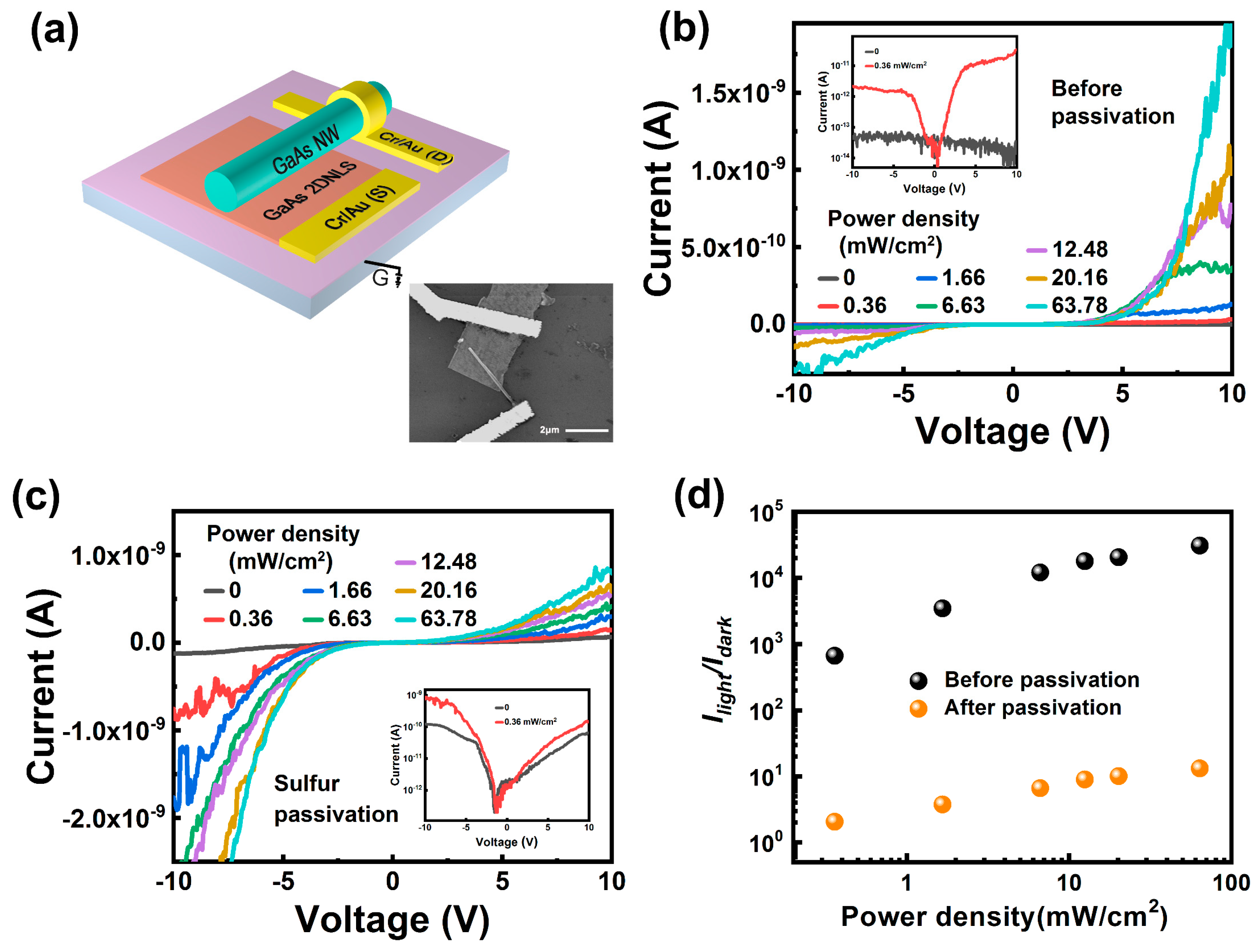
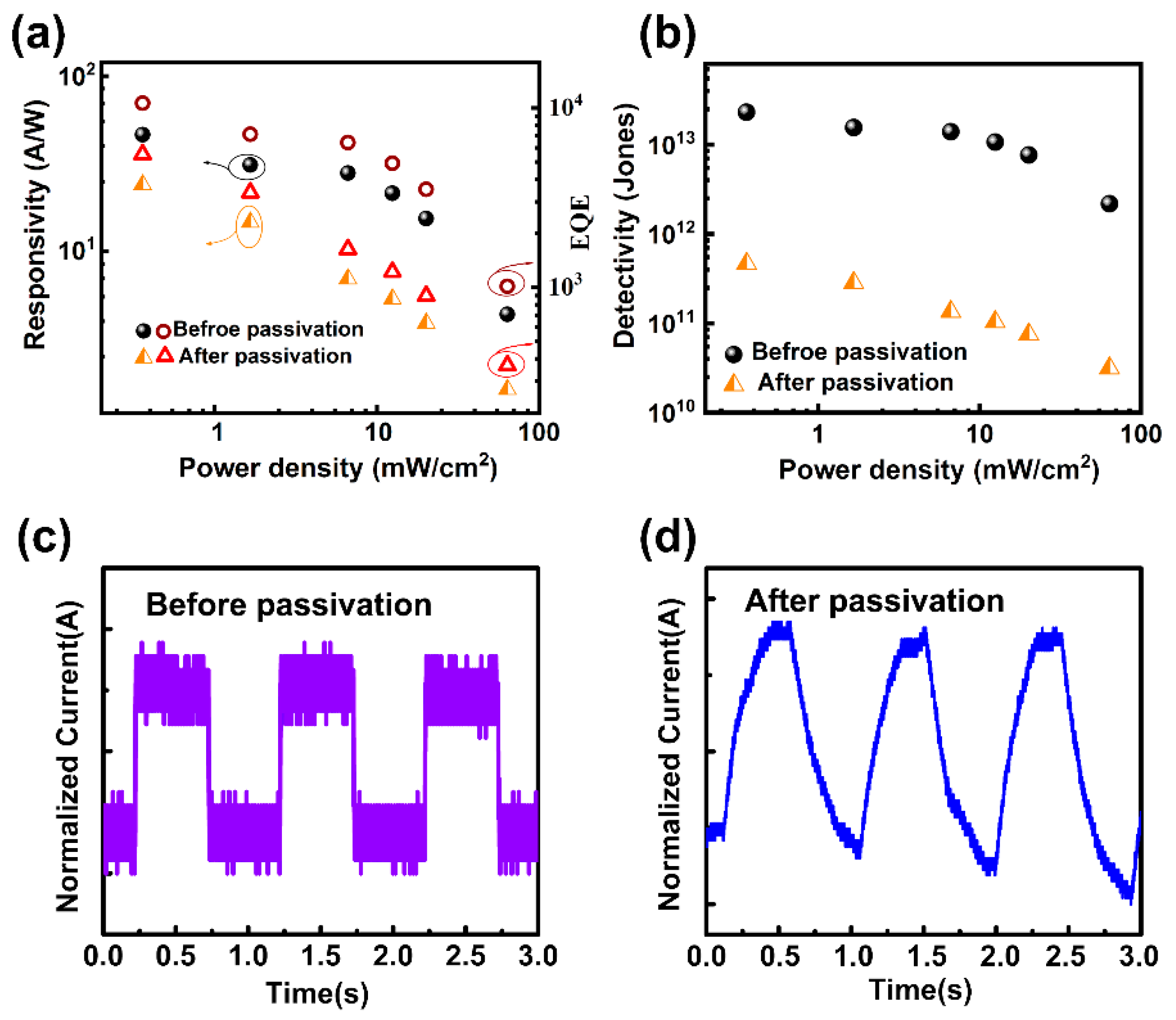
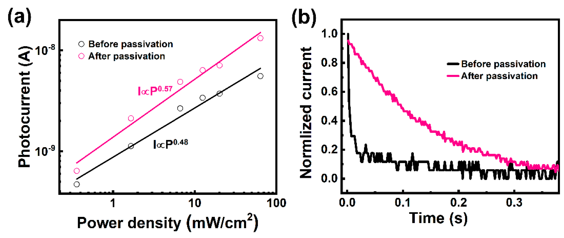
The morphology of GaAs NWs and GaAs 2DNLSs was observed using a transmission electron microscope (TEM), scanning electron microscope (SEM), and atomic force microscope (AFM). The electrical and photo-response properties were characterized by an Agilent 4155C semiconductor parameter analyzer (Agilent Technologies, Inc., Santa Clara, CA, USA). All the measurements for the photodetector were carried out in a vacuum under 532 nm laser illumination at room temperature.

3. Results

Figure 1a shows the morphologies of GaAs NWs measured with the SEM. It can be seen that the nanowires are uniform with a length of about 8.5 μm and a diameter of about 200 nm. Figure 1b shows the TEM image and selected area electron diffraction (SAED) of a single GaAs NW. It is clearly observed that the GaAs NW has excellent crystallinity with a lattice spacing of 0.325 nm along the (111) planes, which is consistent with zinc blended GaAs. Figure 1c shows the AFM image of a GaAs 2DNLS. It can be seen that the thickness of this sheet is about 18 nm with a clean surface, which indicates that the AlAs sacrificial layers were fully removed. According to the TEM and SAED in Figure 1d, the GaAs 2DNLS exhibits a uniform thickness and an excellent crystallinity with zinc blended crystal. According to our previous work, GaAs NWs and GaAs 2DNLSs both exhibit p-type semiconductor characteristics [9,14].
In order to confirm the influence of passivation on surface states, a GaAs 2DNLS photodetector was fabricated and passivated by (NH4)2S. The I-V characteristics of the GaAs 2DNLS photodetector under various power densities before and after passivation are shown in Figure S1. The dependence of the photocurrent and power density was used to analyze the surface states density, as shown in Figure 2a. The relationships were fitted using the equation: IPk, where I is the photocurrent and P is the power density. The k value is used to evaluate the response of the photocurrent to the light power density. It is related to the defects of the material. The larger the k value, the fewer the surface defects of the low-dimensional material [14]. For the GaAs 2DNLS photodetector before passivation, the k value was calculated to be about 0.48. However, the k value increased to 0.57 after passivation. This indicates that the surface states density of GaAs 2DNLS is reduced. Furthermore, the decay time greatly increased after passivation, as shown in Figure 2b. The results are consistent with the passivated GaAs NW photodetector [14].
A mixed-dimensional GaAs photodetector with an electron channel was then fabricated. Figure 3a depicts the schematic diagram and corresponding morphology. The electron channel was constructed utilizing the surface band bending caused by surface states. The effect of the electron channel on response speed is confirmed by surface passivation.
The I-V characteristics curves of the photodetector before and after passivation illuminated with 532 nm laser under different light power densities are detailed in Figure 3b,c. It can be seen that the I-V curve of the unpassivated photodetector exhibits a typical rectification characteristic, which is attributed to the special band structure. The turn-on voltage is about 5 V. Although GaAs NWs and GaAs 2DNLSs have the same electron affinity and almost the same band gap, the surface states density of GaAs 2DNLSs is much larger than that of GaAs NWs. In this case, the degree of downward band bending caused by surface states is also larger than for GaAs NWs. Hence, a special band structure is formed at the interface of GaAs 2DNLSs and GaAs NWs. In this structure, a special band offset with a valence well is constructed. The valence well provides a fast transport channel for photo-generated electrons. Meanwhile, the photo-generated holes in GaAs NWs and GaAs 2DNLSs will diffuse into the main body of these materials. The special band structure can effectively enhance the separation efficiency, reduce the recombination efficiency and improve the response speed of the device. Furthermore, considering the special band structure, the I-V curves exhibit a forward-conducting characteristic.
Figure 3c shows the I-V characteristics of the device after passivation. It can be observed that the current continuously increases with increasing voltage and the I-V curves are symmetrical. This phenomenon is attributed to the reduction or disappearance in the band bending caused by passivation. In this case, when the bias is higher than the Schottky barrier of the electrodes, electrons and holes can be transported in the valence band and conduction band, respectively, and collected by the electrodes. Therefore, the I-V curve does not exhibit a rectification characteristic.
The ratio of photocurrent to dark current (Ilight/Idark) is an important parameter to evaluate the performance of the photodetectors. Figure 3d shows the ratios of photocurrent to dark current before and after passivation at 8 V. It is clearly observed that the Ilight/Idark increases with increasing laser power density. This is because more carriers are generated under the condition of larger laser power density. In addition, the Ilight/Idark of the unpassivated device is much larger than that of the passivated device. This is ascribed to the special band structure of the valence well, which traps the generated electrons to improve the separation efficiency and reduce the recombination efficiency [9]. However, the valence well is removed in the passivated device. Its separation efficiency is smaller than in the unpassivated device. Therefore, the Ilight/Idark of passivated devices is still much smaller than that of unpassivated devices.
Responsivity (R), external quantum efficiency (EQE), and detectivity (D*) are the key parameters used to measure the performance of a detector. These three parameters can be calculated by the following three formulas [3,14].
R = I l i g h t I d a r k P S
E Q E = h c R e λ
D * = R 2 e I dark / S
where Ilight is the photocurrent, Idark is the dark current, P is the laser power density, S is the effective light-sensing area, e is the electron charge, h is the Planck constant, c is the velocity of light, and λ is the wavelength of light. Figure 4a,b shows the responsivity, EQE, and detectivity of the device before and after passivation at 8 V. The maximum responsivity and EQE were found to be 1.06 × 10⁵% and 46.3 AW−1, respectively, at 8 V before passivation. The detectivity is about 2.3 × 10¹³ Jones, which is higher than that of the commercial photodetectors. Note that the responsivity decreases with increasing laser power density. This is due to the competition between the recombination and separation of photo-generated carriers. Under low power density conditions, the increase in carrier separation rate leads to higher responsivity. Under high power density conditions, the carrier recombination rate increases and the responsivity decreases. Moreover, the device exhibits a gain phenomenon, which is attributed to prolongation of carrier lifetime caused by surface states and the interface band structure [21,22,23]. After passivation, the maximum responsivity, EQE, and detectivity are 24.0 AW−1, 5.5 × 10³%, and 4.6 × 10¹¹ Jones, respectively. The responsivity of the device before passivation is about 1.9-fold higher than that after passivation. This is because the special band structure increases the carrier separation efficiency, and the electron trap provides a fast channel for the transmission of photo-generated electrons.
The time-dependent photoresponses were determined under illumination with a 532 nm laser. The response time is defined as the time interval from 10% to 90% (rise time) and from 90% to 10% (decay time) of the current signal [24]. Figure 4c,d shows the response of the device at 8 V before and after passivation, respectively. At 8 V, the rise time of the unpassivated device is about 4.7 ms. However, for passivated devices, the rise time increases to 210 ms, which is 45-fold longer than that of the as-prepared device. The performance of our device was compared with state-of-the-art low-dimensional GaAs photodetectors, as shown in Table 1. For the as-prepared device, an electron channel exists at the interface, which accelerates the electron transport. After passivation, the surface band bending decreases; the valence well at the interface disappears or becomes weaker; and the one-dimensional fast electron transmission channel disappears. Hence, the response time of the device greatly increases.
Figure 5a shows a comparison of the decay time at 8 V for the device before and after passivation. The decay time is about 6.1 ms for the unpassivated photodetector and about 373.7 ms for the passivated device. The decay time of the passivated device is about 61-old longer than that of the unpassivated device. This result can be explained by the special band structure of this device, as shown in Figure 5b [28]. It is well-known that the decay time is affected by the carrier recombination process [29,30]. After passivation, the band bending at the interface decreases and the valence well and holes barrier tend to disappear. Meanwhile, the restriction of the one-dimensional electron transmission channel is weakened. Hence, the electron transport speed is reduced and the carrier recombination efficiency enhanced. As a result, the response time of the device increases.

4. Conclusions

In summary, a fast-response mixed-dimensional GaAs photodetector was fabricated using a GaAs NW and GaAs 2DNLS. An electron transmission channel and a special band structure form at the interface between the GaAs NW and GaAs 2DNLS in this device. The channel provides a high-speed path for electron transport. As a result, the device exhibits a rise time of 4.7 ms and decay time of 6.1 ms at 8 V. Meanwhile, its responsivity is as high as 46.3 AW−1. Furthermore, sulfur passivation treatment is applied to verify the function of the transmission channel on fast response. After passivation, the rise time increases to 210 ms and the decay time increases to 373.7 ms, which are much longer than those before passivation. This work is of great significance for fabricating fast response photodetectors and utilizing surface states.

Supplementary Materials

The following are available online at https://www.mdpi.com/article/10.3390/cryst11101160/s1, Figure S1: The I-V characteristic curves of the GaAs 2DNLS photodetector under different power densities (a) before and (b) after passivation.

Author Contributions

Methodology, S.G., X.C., D.F. and J.T.; writing—original draft, S.G.; investigation, X.C.; conceptualization, D.W.; writing—review and editing, D.W.; formal analysis, X.F.; resources, L.L.; supervision, Z.W.; project administration, Z.W. All authors have read and agreed to the published version of the manuscript.

Funding

This work is supported by the National Natural Science Foundation of China under grant Nos. 62074018, 12074045, and 61904017; the Developing Project of Science and Technology of Jilin Province under grant No. 20200301052RQ; and the Project of Education Department of Jilin Province under grant Nos. JJKH20200763KJ and JJKH20210831KJ.

Conflicts of Interest

The authors declare no conflict of interest.

References

  1. Luo, Y.; Yan, X.; Zhang, X.; Zhang, M.; Ren, X. Enhanced performance of graphene/GaAs nanowire photoelectric conversion devices by improving the Schottky barrier height. J. Vac. Sci. Technol. B 2019, 37, 051202. [Google Scholar] [CrossRef]
  2. Xu, X.; Wang, H. Resonant energy transfer between patterned InGaN/GaN quantum wells and CdSe/ZnS quantum dots. Nanoscale 2016, 8, 342–347. [Google Scholar] [CrossRef]
  3. Luo, T.; Lian, B.; Liu, Z.; Xie, X.; Lou, Z.; Shen, G. Single-GaSb-nanowire-based room temperature photodetectors with broad spectral response. Sci. Bull. 2015, 60, 101–108. [Google Scholar] [CrossRef] [Green Version]
  4. Michel, J.; Liu, J.; Kimerling, L.C. High-performance Ge-on-Si photodetectors. Nat. Photonics 2010, 4, 527–534. [Google Scholar] [CrossRef]
  5. Zheng, D.; Wang, J.; Hu, W.; Liao, L.; Fang, H.; Guo, N.; Wang, P.; Gong, F.; Wang, X.; Fan, Z.; et al. When Nanowires Meet Ultrahigh Ferroelectric Field-High-Performance Full-Depleted Nanowire Photodetectors. Nano Lett. 2016, 16, 2548–2555. [Google Scholar] [CrossRef]
  6. Sun, L.; Wang, C.; Xu, L.; Wang, J.; Liu, X.; Chen, X.; Yi, G.C. SbSI whisker/PbI2 flake mixed-dimensional van der Waals heterostructure for photodetection. Cryst. Eng. Comm. 2019, 21, 3779–3787. [Google Scholar] [CrossRef]
  7. Lee, Y.T.; Jeon, P.J.; Han, J.H.; Ahn, J.; Lee, H.S.; Lim, J.Y.; Choi, W.K.; Song, J.D.; Park, M.C.; Im, S.; et al. Mixed-Dimensional 1D ZnO-2D WSe2 van der Waals Heterojunction Device for Photosensors. Adv. Funct. Mater. 2017, 27, 1703822. [Google Scholar] [CrossRef]
  8. Liao, L.; Lin, Y.C.; Bao, M.; Cheng, R.; Bai, J.; Liu, Y.; Qu, Y.; Wang, K.L.; Huang, Y.; Duan, X. High-speed graphene transistors with a self-aligned nanowire gate. Nature 2010, 467, 305–308. [Google Scholar] [CrossRef]
  9. Wang, D.; Chen, X.; Fang, X.; Tang, J.; Lin, F.; Wang, X.; Liu, G.; Liao, L.; Ho, J.C.; Wei, Z. Photoresponse improvement of mixed-dimensional 1D-2D GaAs photodetectors by incorporating constructive interface states. Nanoscale 2021, 13, 1086–1092. [Google Scholar] [CrossRef] [PubMed]
  10. Boland, J.L.; Casadei, A.; Tutuncuoglu, G.; Matteini, F.; Davies, C.L.; Jabeen, F.; Joyce, H.J.; Herz, L.M.; Fontcuberta, M.A.; Johnston, M.B. Increased Photoconductivity Lifetime in GaAs Nanowires by Controlled n-Type and p-Type Doping. ACS Nano 2016, 10, 4219–4227. [Google Scholar] [CrossRef] [Green Version]
  11. Luo, L.B.; Chen, J.J.; Wang, M.Z.; Hu, H.; Wu, C.Y.; Li, Q.; Wang, L.; Huang, J.A.; Liang, F.X. Near-Infrared Light Photovoltaic Detector Based on GaAs Nanocone Array/Monolayer Graphene Schottky Junction. Adv. Funct. Mater. 2014, 24, 2794–2800. [Google Scholar] [CrossRef]
  12. Shen, L.; Pun, E.Y.B.; Ho, J.C. Recent developments in III–V semiconducting nanowires for high-performance photodetectors. Mater. Chem. Front. 2017, 1, 630–645. [Google Scholar] [CrossRef]
  13. Chang, C.C.; Chi, C.Y.; Yao, M.; Huang, N.; Chen, C.C.; Theiss, J.; Bushmaker, A.W.; Lalumondiere, S.; Yeh, T.W.; Povinelli, M.L.; et al. Electrical and optical characterization of surface passivation in GaAs nanowires. Nano Lett. 2012, 12, 4484–4489. [Google Scholar] [CrossRef] [PubMed]
  14. Chen, X.; Xia, N.; Yang, Z.; Gong, F.; Wei, Z.; Wang, D.; Tang, J.; Fang, X.; Fang, D.; Liao, L. Analysis of the influence and mechanism of sulfur passivation on the dark current of a single GaAs nanowire photodetector. Nanotechnology 2018, 29, 095201. [Google Scholar] [CrossRef]
  15. Wang, Z.L.; Hao, Z.B.; Yu, J.D.; Wu, C.; Wang, L.; Wang, J.; Sun, C.Z.; Xiong, B.; Han, Y.J.; Li, H.T.; et al. Manipulating the Band Bending of InGaN/GaN Quantum Dots in Nanowires by Surface Passivation. J. Phys. Chem. C. 2017, 121, 6380–6385. [Google Scholar] [CrossRef]
  16. van Tilburg, J.W.W.; Algra, R.E.; Immink, W.G.G.; Verheijen, M.; Bakkers, E.P.A.M.; Kouwenhoven, L.P. Surface passivated InAs/InP core/shell nanowires. Semicond. Sci. Technol. 2010, 25, 024011. [Google Scholar] [CrossRef] [Green Version]
  17. Lee, H.Y.; Lu, D.E.; Lee, C.T. Performance improvement of GaN-based ultraviolet metal–semiconductor–metal photodetectors using chlorination surface treatment. J. Vac. Sci. Technol. B Microelectron. Nanometer. Struct. 2012, 30, 031211. [Google Scholar] [CrossRef]
  18. Kang, Y.; Tang, J.L.; Wang, P.; Lin, F.; Fang, X.; Fang, D.; Wang, D.; Wang, X.; Wei, Z. High density GaAs nanowire arrays through substrate processing engineering. Mater. Res. Express 2018, 6, 035012. [Google Scholar] [CrossRef]
  19. Tao, P.; Yao, S.; Liu, F.; Wang, B.; Huang, F.; Wang, M. Recent advances in exfoliation techniques of layered and non-layered materials for energy conversion and storage. J. Mater. Chem. A 2019, 7, 23512–23536. [Google Scholar] [CrossRef]
  20. Yoon, J.; Jo, S.; Chun, I.S.; Jung, I.; Kim, H.S.; Meitl, M.; Menard, E.; Li, X.; Coleman, J.J.; Paik, U.; et al. GaAs photovoltaics and optoelectronics using releasable multilayer epitaxial assemblies. Nature 2010, 465, 329–333. [Google Scholar] [CrossRef] [PubMed]
  21. Soci, C.; Zhang, A.; Xiang, B.; Dayeh, S.A.; Aplin, D.P.R.; Park, J.; Bao, X.Y.; Lo, Y.H.; Wang, D. ZnO nanowire UV photodetectors with high internal gain. Nano Lett. 2007, 7, 1003–1009. [Google Scholar] [CrossRef]
  22. Gong, M.G.; Kirkeminde, A.; Xie, Y.; Lu, R.T.; Liu, J.W.; Wu, J.Z.; Ren, S.Q. Iron pyrite (FeS2) broad spectral and magnetically responsive photodetectors. Adv. Opt. Mater. 2013, 1, 78–83. [Google Scholar] [CrossRef]
  23. Wei, H.T.; Fang, Y.J.; Yuan, Y.B.; Shen, L.; Huang, J.S. Trap engineering of CdTe nanoparticle for high gain, fast response, and low noise P3HT:CdTe nanocomposite photodetectors. Adv. Mater. 2015, 27, 4975–4981. [Google Scholar] [CrossRef]
  24. Wu, Y.; Yan, X.; Zhang, X.; Ren, X. A monolayer graphene/GaAs nanowire array Schottky junction self-powered photodetector. Appl. Phys. Lett. 2016, 109, 183101. [Google Scholar] [CrossRef]
  25. Ali, H.; Zhang, Y.Y.; Tang, J.; Peng, K.; Sun, S.B.; Sun, Y.; Song, F.L.; Falak, A.; Wu, S.Y.; Qian, C.J.; et al. High-responsivity photodetection by a self-catalyzed phase-pure p-GaAs nanowire. Small 2018, 14, 1704429. [Google Scholar]
  26. Zhu, X.; Lin, F.; Zhang, Z.; Chen, X.; Huang, H.; Wang, D.; Tang, J.; Fang, X.; Fang, D.; Ho, J.C.; et al. Enhancing Performance of a GaAs/AlGaAs/GaAs Nanowire Photodetector Based on the Two-Dimensional Electron-Hole Tube Structure. Nano Lett. 2020, 20, 2654–2659. [Google Scholar] [CrossRef] [PubMed]
  27. Chen, X.; Jiang, B.; Wang, D.; Li, G.; Wei, Z. Gate-tunable the interface properties of GaAs–WSe2 (1D–2D) vdWs heterojunction for high-responsivity, self-powered photodetector. Appl. Phys. Lett. 2021, 118, 041102. [Google Scholar] [CrossRef]
  28. Milines, A.G.; Feucht, D.L. Heterojunction and Metal-Semiconductor Junction; Academic Press: New York, NY, USA, 1972. [Google Scholar]
  29. Bera, A.; Basak, D. Carrier relaxation through two-electron process during photoconduction in highly UV sensitive quasi-one-dimensional ZnO nanowires. Appl. Phys. Lett. 2008, 93, 053102. [Google Scholar] [CrossRef]
  30. Liu, H.Y.; Hsu, W.C.; Chou, B.Y.; Wang, Y.H. A Simple Passivation Technique for AlGaN/GaN Ultraviolet Schottky Barrier Photodetector. IEEE Photonics Technol. Lett. 2014, 26, 138–141. [Google Scholar] [CrossRef]
Figure 1. (a) Top-view SEM image of GaAs NWs, (b) TEM image of GaAs NW; the insert is the SAED (c) AFM image of GaAs 2DNLS, (d) TEM image of GaAs 2DNLS; the insert is the SAED of GaAs 2DNLS.
Crystals 11 01160 g001
Figure 2. (a) Dependence of photocurrent and power intensity before and after passivation. (b) Time-dependent current decay curve of GaAs 2DNLS photodetector before and after passivation.
Crystals 11 01160 g002
Figure 3. (a) Schematic illustration of mixed-dimensional GaAs photodetector; insert is the SEM image of the same. The I-V characteristics curves of the devices under different power densities (b) before and (c) after passivation. The inserts are dark currents and photocurrents at 0.36 mW/cm2 on a logarithmic scale. (d) Ratios of photocurrent to dark current before and after passivation under different power densities at 8 V.
Crystals 11 01160 g003
Figure 4. The (a) responsivity, EQE, and (b) detectivity of the detector under different laser power densities at 8 V before and after passivation. The time-dependent response of the photodetector (c) before and (d) after passivation at 8 V.
Crystals 11 01160 g004
Figure 5. (a) Comparison of the decay time before and after passivation at 8 V. (b) Band structure of the mixed-dimensional GaAs photodetector before and after passivation.
Crystals 11 01160 g005
Table 1. Comparison of the performance parameters for low-dimensional GaAs photodetectors.
MaterialR (mA/W)τrd (ms)Reference
GaAs NW1.82 × 104-/188[14]
Passivated GaAs NW2.5 × 104-/269[14]
Pure-phase GaAs NW1.45 × 108-[25]
GaAs/AlGaAs/GaAs NW570175/190[26]
GaAs NW/WSe2511246/280[27]
Graphene/GaAs NW3010.042/0.14[1]
GaAs NW/GaAs 2DNLS4.63 × 1044.7/6.1this work
Publisher’s Note: MDPI stays neutral with regard to jurisdictional claims in published maps and institutional affiliations.

