Article

Grating Coupler Design for Vertical Light Coupling in Silicon Thin Films on Lithium Niobate

1
College of Electric and Electronic Engineering, Zibo Vocational Institute, Zibo 255314, China
2
School of Physics, Shandong University, Jinan 250100, China
3
College of New Materials and New Energies, Shenzhen Technology University, Shenzhen 518118, China
*
Author to whom correspondence should be addressed.
Crystals 2020, 10(9), 850; https://doi.org/10.3390/cryst10090850
Submission received: 10 August 2020 / Revised: 18 September 2020 / Accepted: 21 September 2020 / Published: 22 September 2020

Abstract

:
In this paper we provide a design for a vertical grating coupler for a silicon thin film on lithium niobate. The parameters-such as the cladding layer thickness of lithium niobate, fiber position, fiber angle, grating period, and duty cycle are analyzed and optimized to reduce the mode mismatch loss and the internal reflections. The alignment tolerances, for the grating coupler parameters, are also simulated and evaluated. We determine that our simulated grating coupler exhibits high efficiency, enhanced light coupling, and high alignment tolerance.

Graphical Abstract

1. Introduction

In dense photonic integration, highly developed silicon (Si) platforms have attained numerous substantial successes. The advantages of this mature technology are their low optical absorption, large refractive index contrast, and high compatibility with semiconductor technology [1]. However, single-crystal Si is a centrally symmetric crystal that has no linear electro-optic effect, piezo-electric or other similar properties. As a result, the Si material has limitations in its application to integrated optics. An alternative is lithium niobate (LiNbO3, LN) crystal, which is more promising in this role [2,3,4] because of its wide transparency range and excellent electro-optic, nonlinear, acousto-optic, piezoelectric, photorefractive, and elasto-optic properties. However, contrary to photonics based on Si, the manufacturing of LN photonic devices is still in its infancy. The integration of a Si thin film on a thin LN cladding layer, combines the mature micro- and nano- technology properties of Si and the optical properties of LN. This produces an enhanced optical material that has a good confinement, and strong guidance, of light due to the high-refractive-index contrast between Si and LN [5,6]. When the light propagates in the Si waveguide, the energy of the light is distributed within both the Si thin film and the LN layer. Electro-optic modulators in Si on LN can be prepared by applying voltage to the LN layer [7,8,9,10,11]. Previously, based on a hybrid Si/LN material, many photonic devices have been developed such as Mach-Zehnder interferometer [7,8], photonic crystals [9] and micro-ring resonator [10,11].
Due to the substantial light mode mismatch between the sub-micron-sized optical material devices and single-mode fibers, the coupling efficiency between them is very low; this will impede improvement in performance of the optical device. An effective method, which requires no end-face polishing, for the coupling of fibers and optical devices is known as grating coupling [12,13,14,15,16,17]. Many previous articles report on the grating coupler in silicon on insulator (SOI) [12,13,14] and lithium niobate on insulator (LNOI) [15,16,17], but few reports investigate a grating coupler for a Si thin film on LN.
In this study, a grating coupler for a Si thin film on LN was simulated and analyzed. This scheme, based on the three-dimension finite-difference time-domain method (3D-FDTD) [18], involved the cladding layer thickness of LN thin film (T), fiber position x (separation of the x-axis between grating edge and the fiber core, Lx), fiber position y (separation of the y-axis between grating upper surface and the fiber core, Ly), fiber position z (separation of the z-axis between grating centerline and the fiber core, Lz), fiber angle (θ), grating period (Λ), and duty cycle (DC, defined as the fraction of the ridge width within the period). All these parameters were investigated so that guidance on the improvement of the coupling efficiency of the grating coupler could be provided. The tolerances of the grating coupler, which was significantly important for any practical implementation of such a device, were also carefully studied.

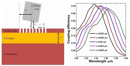
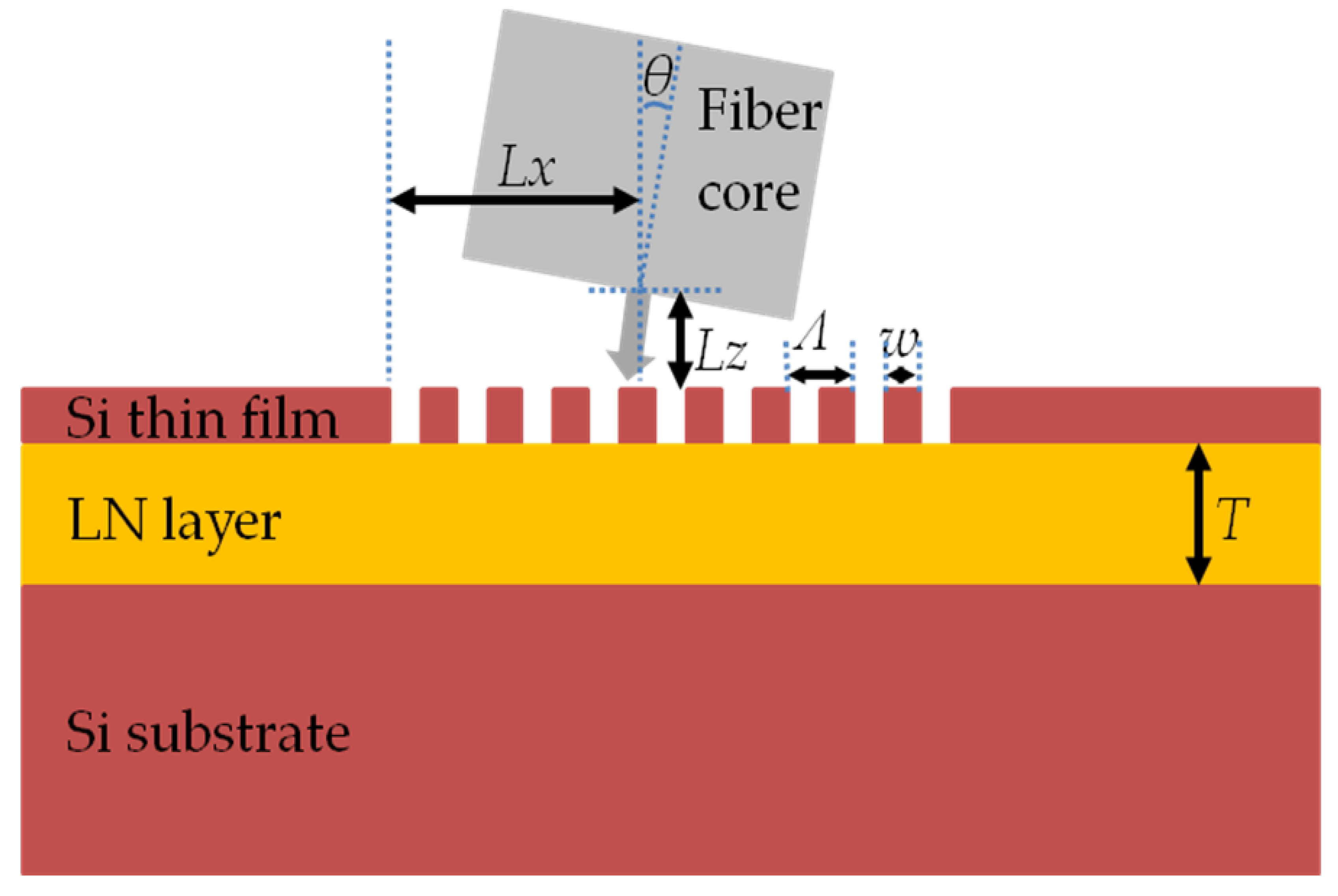
2. Device Design and Methods

The Si thin film on LN that was studied moving from the highest to the lowest layer involved a 0.22 μm-thick Si thin film [19,20], a z-cut LN film, and a Si substrate. The schematic cross-section of which, including the grating coupler is shown in Figure 1. We simulated coupling process between the optical fiber and the grating coupler for the fiber fundamental transverse electric mode (TE0) as a source. In this simulation, the thickness of the Si thin film and the etch depth were all chosen to be 0.22 μm; the parameters T, Lx, Ly, Lz, θ, Λ, and DC were varied to maximize the light from the single-mode fiber coupling into the waveguide.
The Bragg phase matching condition was the basic equation of grating couplers. The coupling modes were resonantly excited when the conditions were met. For an infinitely long grating, the equation was given by [21]:
k sinθ = β + q2π/Λ,
where k = 2π/λ is the wavenumber, θ is the incident angle, q is the diffraction order (here q = −1), Λ is the grating period, β = 2πneff is the real part of the propagation constant and neff is the effective index of the guided mode in the grating coupler. The above equation was used to obtain the range of grating periods (Λ).
In order to avoid a high second order reflection at the grating-waveguide interface, θ was chosen to be 8° [21]. The effective refractive index should fulfill the inequality nLNneffnSi, where nLN/nSi was the refractive index of LN (2.138)/Si (3.478). By substituting the inequality into Equation (1), an estimated range of Λ with respect to the fiber angle would be obtained: λ/(3.478 − sinθ) ≤ Λλ/(2.138 − sinθ). The Λ could be in the estimated range of 0.465 μm ≤ Λ ≤ 0.775 μm.
The grating coupling mechanism was shown as follows: light was coupled in the waveguide plane, from the single-mode fiber, due to the diffraction effect of the grating coupled to the periodic grating structure; when the input field mode was adjusted to match the fiber mode, light coupled effectively into the waveguide plane from the single-mode fiber. Coupling efficiency was defined as the ratio of the power converted to the waveguide plane to the source power. The parameters for the grating coupler were optimized to reduce the mode mismatch between the waveguide optical devices and the single-mode fibers. We performed simulations and optimizations using a 3D-FDTD method and a perfectly matched layer (PML) boundary conditions [22].

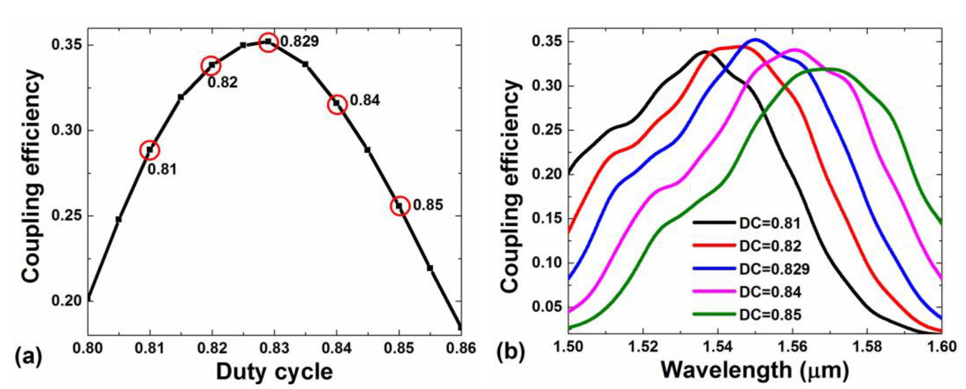
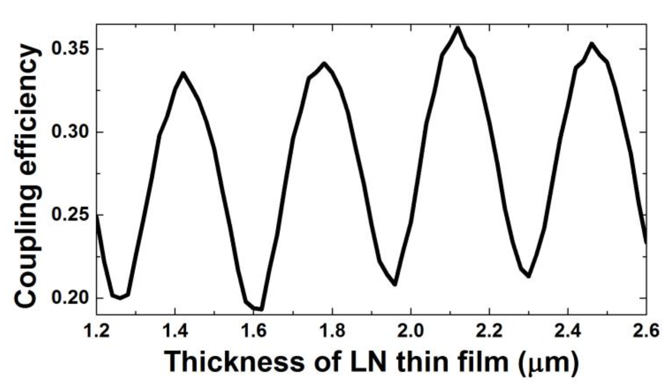
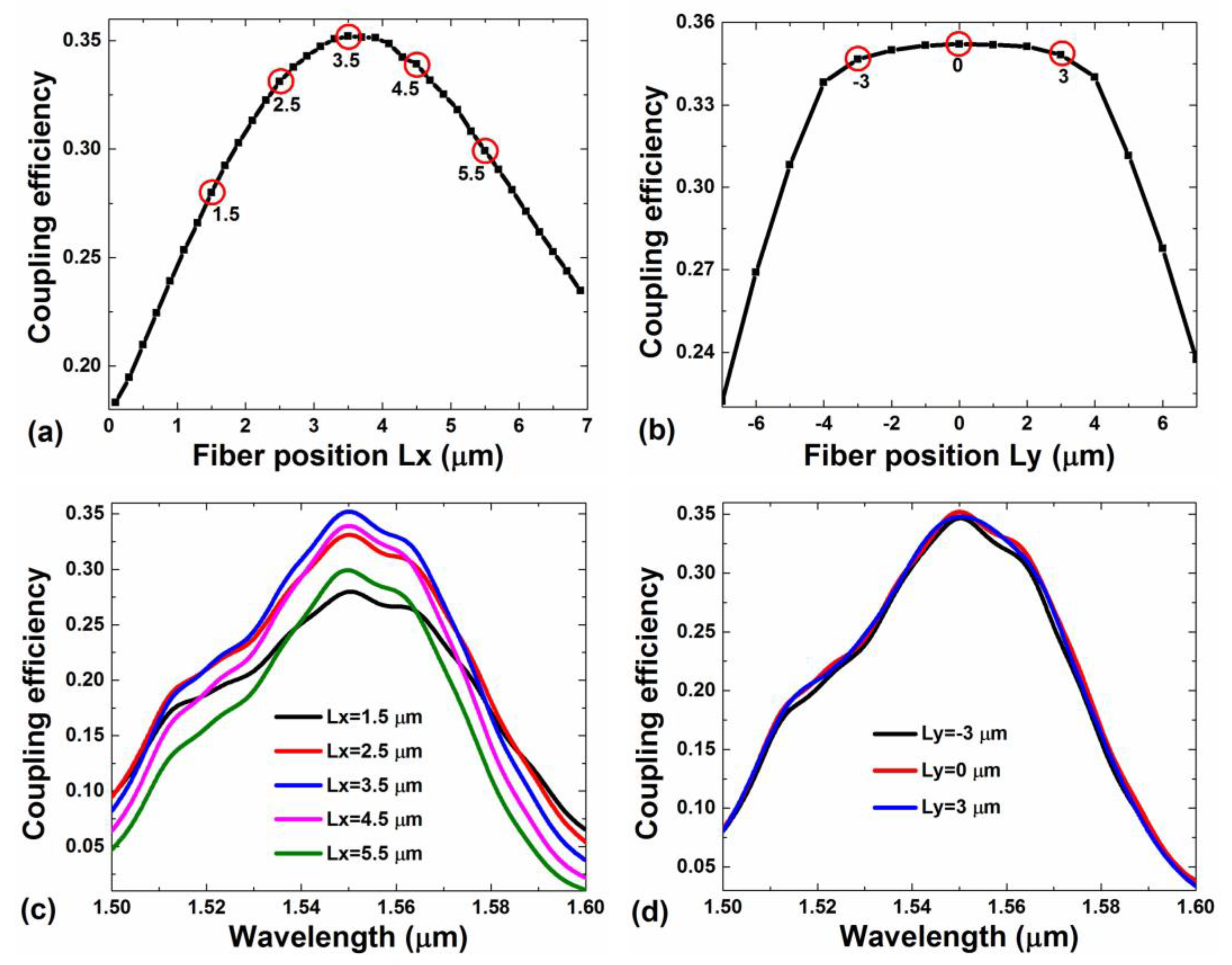
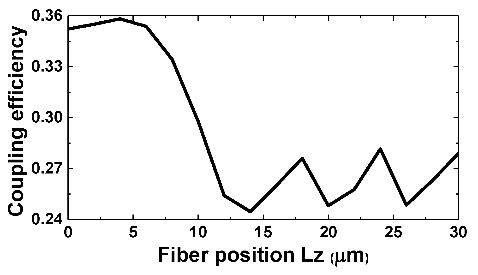
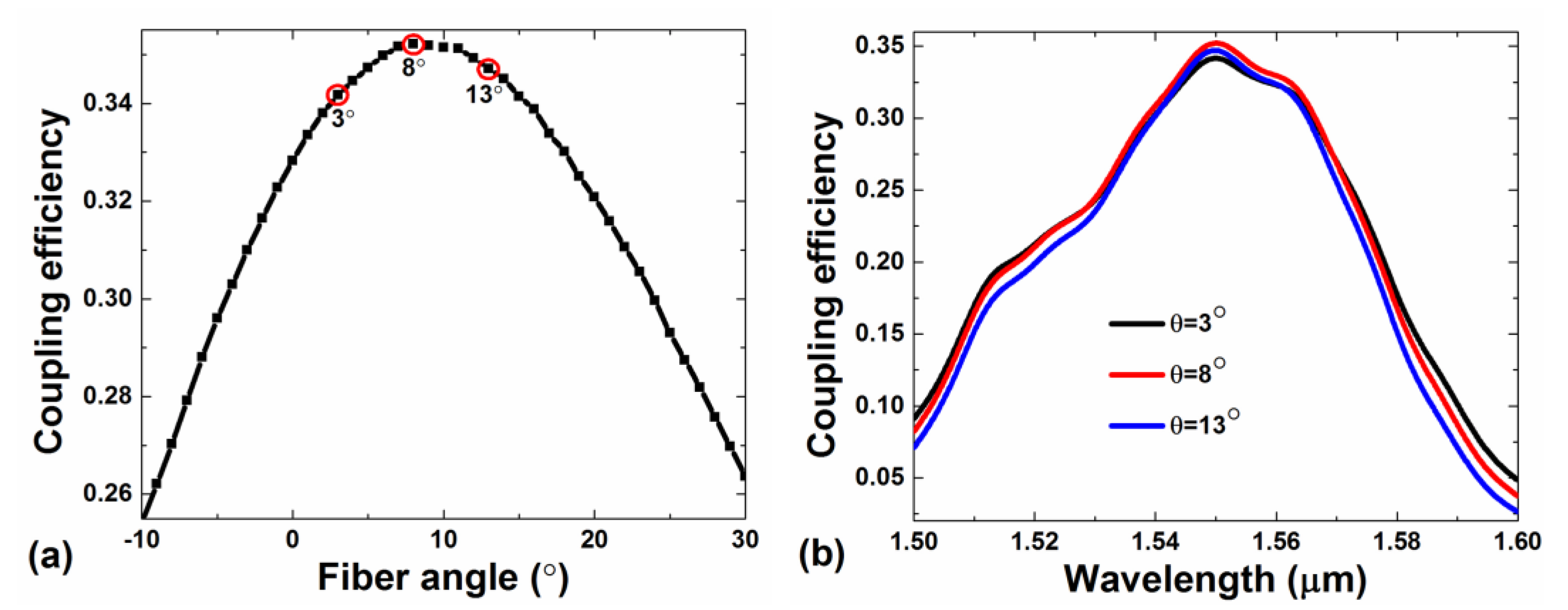
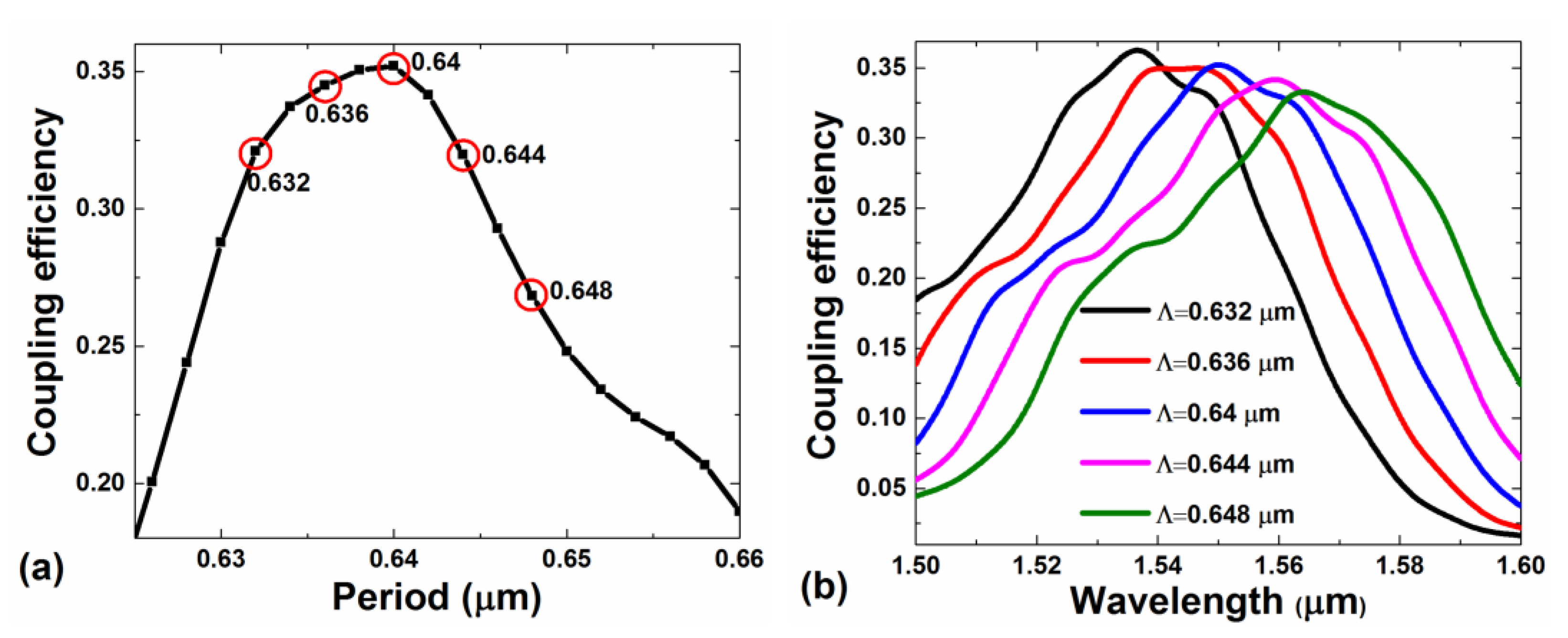
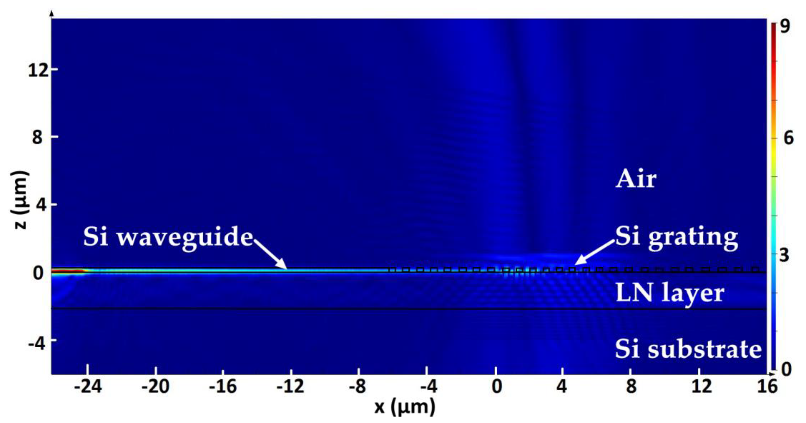
3. Results and Discussion

To determine an enhanced coupling efficiency, the parameters for the design of the grating coupler need to be carefully analyzed. At a wavelength of light of 1.55 μm, a Si thin film thickness of 0.22 μm, and an etch depth of 0.22 μm, the parameters of the grating coupler for TE polarization were simulated and optimized. The results of which are shown in Table 1. In this work, the control variable method was used to study the influence of each parameter on the performance of the grating coupler. During the simulation, other parameters were fixed to their optimized value and only the studied parameters were modified.
Figure 2 shows the relationship between the coupling efficiency and thickness of the LN cladding layer for a TE polarization. With varying cladding layer thickness of the LN, the curve of coupling efficiency oscillated between the minimum and the maximum, as described in [23] and [24]. A possible reason for this was explained as follows. As a beam of light from the fiber was diffracted by the grating coupler, part of the light beam was scattered towards the LN cladding layer. At the LN/Si substrate interface, a part of the power was transmitted into the Si substrate and a part of it was reflected. The reflected part propagated upward again through the LN cladding layer toward grating. The LN cladding layer thickness should be chosen such that the reflected light and the incident light met the phase matching condition. The T at high coupling efficiency was determined via the parameters of Lx, Ly, Lz, θ, Λ, DC, λ, etc. In the following simulation, the T was selected to be 2.1 μm.
To study the tolerance of Lx and Ly, the simulations for the coupling efficiency as a function of wavelength for varying Lx and Ly were performed. Figure 3a,b show this coupling efficiency as a function of Lx and Ly, respectively. When the Lx was set at 3.5 μm and Ly was at 0 μm, the coupling efficiency was at a maximum. With a 2 μm deviation in Lx, the coupling efficiency descended a little. When the deviation of Ly was smaller than 4 μm, the coupling efficiency was almost unchanged; when larger than 4 μm, the coupling efficiency sharply descended, at an increased rate as the Ly deviation increased. Figure 3c,d corresponding to the red circles in Figure 3a,b show the coupling efficiency as a function of wavelength for different Lx and Ly, respectively. For an increasing wavelength, the coupling efficiency increased at first and but then decreased after reaching the peak at a wavelength of 1.55 μm.
Figure 4 shows this coupling efficiency as a function of Lz. When Lz was smaller than 8 μm, the curve of coupling efficiency had little fluctuation. When Lz was larger than 8 μm, the coupling efficiency descended because light from fiber to grating scattered.
Figure 5a illustrates the coupling efficiency as a function of fiber angle. To reduce back reflections, the incident angle was optimized at 8° in Figure 5a. With an increasing deviation from this fiber angle, the coupling efficiency descended slowly. Figure 5b shows coupling efficiency as a function of wavelength for different fiber angles, corresponds to the red circles in Figure 5a. At λ = 1.55 μm, for incident angle θ = 3°, 8°, and 13°, the coupling efficiencies were 34.17%, 35.21%, and 34.71%, respectively.
Coupling efficiency as a function of period is shown in Figure 6a. A grating period of 0.64 μm provided the peak coupling efficiency; the coupling efficiency decreased whenever the grating period increased or decreased from this position. When the grating period deviated by 0.004 and 0.008 μm, the coupling efficiency decreased a minuscule amount at a wavelength of 1.55 μm. Figure 6b shows coupling efficiency as a function of wavelength for different periods, which corresponds to the red circles in Figure 6a. The peak coupling efficiency was red shifted with an increasing period.
Coupling efficiency as a function of duty cycle is illustrated in Figure 7a. A grating duty cycle of 0.829 provided a peak coupling efficiency. For 0.019 and 0.021 deviation of the duty cycle at a wavelength of 1.55 μm, the change in coupling efficiency was tiny. Figure 7b shows the coupling efficiency as a function of wavelength for different duty cycle, corresponds to the red circles in Figure 7a. The peak coupling efficiency was red shifted with an increasing duty cycle.
The electric field distribution is shown in Figure 8. The in-coupled light formed an angle (8°) relative to the surface that was perpendicular to the Si substrate. Grating couplers that operated at around 1.55 μm could achieve near-vertical coupling with the waveguide plane also and avoid a high amount of reflection. The light was mainly divided into three parts: one scattered upwards, one coupled into the waveguide, and the other lost into the substrate.

4. Conclusions

In conclusion, the performance of a grating coupler, with vertical light coupling, from a single-mode fiber to a waveguide in a 0.22 μm-thick Si thin film on LN was systematically studied by using a 3D-FDTD simulation technique. The parameters T, Lx, Ly, θ, Λ, and DC were analyzed and found to be optimized at 2.1 μm, 3.5 μm, 0 μm, 8°, 0.64 μm, and 0.829, respectively. A maximum of 35.2% was found for the coupling efficiency. The tolerances of the grating coupler parameters were discussed with respect to the coupling efficiency. A Si thin film on LN is being researched and fabricated at the research centre of Nanoln. Our simulation results on the grating couplers for such an optical device will provide useful guidance to laboratory work such as this.

Author Contributions

B.X. conceived the original idea; H.H. carried out the simulations, analyzed the data, and wrote the paper; B.X. and H.H. contributed the useful and deep discussions and modified the manuscript. All authors have read and agreed to the published version of the manuscript.

Funding

This research was funded by the Shenzhen Science and Technology Planning (NO. JCYJ20190813103207106), the Project of Youth Innovative Talents in Higher Education Institutions of Guangdong (NO. 2018KQNCX399), the Foundation of Zibo Vocational Institute (NO. 2018zzzr03), and the School City Integration Development Plan of Zibo (NO. 2019ZBXC127).

Conflicts of Interest

The authors declare no conflict of interest.

References

  1. Witzens, J.; Baehr-Jones, T.; Hochberg, M. Silicon photonics: On-chip OPOs. Nat. Photonics 2010, 4, 10–12. [Google Scholar] [CrossRef]
  2. Weis, R.S.; Gaylord, T.K. Lithium niobate: Summary of physical properties and crystal structure. Appl. Phys. A 1985, 37, 191–203. [Google Scholar] [CrossRef]
  3. Lawrence, M. Lithium niobate integrated optics. Rep. Prog. Phys. 1993, 56, 363–429. [Google Scholar] [CrossRef]
  4. Syms, R.R.A. Advances in channel waveguide lithium niobate integrated optics. Opt. Quant. Electron. 1988, 20, 189–213. [Google Scholar] [CrossRef]
  5. Rao, A.; Fathpour, S. Compact lithium niobate electrooptic modulators. IEEE J. Sel. Top. Quantum Electron. 2018, 24, 340014. [Google Scholar] [CrossRef]
  6. Rao, A.; Fathpour, S. Heterogeneous thin-film lithium niobate integrated photonics for electrooptics and nonlinear optics. IEEE J. Sel. Top. Quantum Electron. 2018, 24, 8200912. [Google Scholar] [CrossRef]
  7. Chiles, J.; Fathpour, S. Mid-infrared integrated waveguide modulators based on silicon-on-lithium-niobate photonics. Optica 2014, 1, 350–355. [Google Scholar] [CrossRef]
  8. Cao, L.; Aboketaf, A.; Wang, Z.; Preble, S. Hybrid amorphous silicon (a-Si:H)–LiNbO3 electro-optic modulator. Opt. Commun. 2014, 330, 40–44. [Google Scholar] [CrossRef]
  9. Witmer, J.D.; Hill, J.T.; Safavi-Naeini, A.H. Design of nanobeam photonic crystal resonators for a silicon-on-lithium-niobate platform. Opt. Express 2016, 24, 5876. [Google Scholar] [CrossRef] [Green Version]
  10. Witmer, J.D.; Valery, J.A.; Arrangoiz-Arriola, P.; Sarabalis, C.J.; Hill, J.T.; Safavi-Naeini, A.H. High-Q photonic resonators and electro-optic coupling using silicon-on-lithium-niobate. Sci. Rep. 2016, 7, 46313. [Google Scholar] [CrossRef] [Green Version]
  11. Han, H.; Xiang, B. Simulation and analysis of electro-optic tunable microring resonators in silicon thin film on lithium niobate. Sci. Rep. 2019, 9, 6302. [Google Scholar] [CrossRef] [PubMed]
  12. Schmid, B.; Petrov, A.; Eich, M. Optimized grating coupler with fully etched slots. Opt. Express 2009, 17, 11066–11076. [Google Scholar] [PubMed]
  13. Laere, F.V.; Roelkens, G.; Ayre, M.; Schrauwen, J.; Taillaert, D.; Thourhout, D.V.; Krauss, T.F.; Baets, R. Compact and highly efficient grating couplers between optical fiber and nanophotonic waveguides. J. Lightw. Technol. 2007, 25, 151–156. [Google Scholar] [CrossRef] [Green Version]
  14. Roelkens, G.; Vermeulen, D.; Thourhout, D.V.; Baets, R.; Brision, S.; Lyan, P.; Gautier, P.; Fédéli, J.M. High efficiency diffractive grating couplers for interfacing a single mode optical fiber with a nanophotonic silicon-on-insulator waveguide circuit. Appl. Phys. Lett. 2008, 92, 131101. [Google Scholar] [CrossRef] [Green Version]
  15. Chen, Z.; Wang, Y.; Jiang, Y.; Kong, R.; Hu, H. Grating coupler on single-crystal lithium niobate thin film. Opt. Mater. 2017, 72, 136–139. [Google Scholar] [CrossRef]
  16. Cai, L.; Piazza, G. Low-loss chirped grating for vertical light coupling in lithium niobate on insulator. J. Opt. 2019, 21, 065801. [Google Scholar] [CrossRef]
  17. Nisar, M.S.; Zhao, X.; Pan, A.; Yuan, S.; Xia, J. Grating coupler for an on-chip lithium niobate ridge waveguide. IEEE Photonics J. 2017, 9, 1–8. [Google Scholar] [CrossRef]
  18. Tavlove, A.; Hagness, S.C. Computational Electrodynamics: The Finite-Difference Time-Domain Method, 3rd ed.; Artech House: Norwood, MA, USA, 2005. [Google Scholar]
  19. Matthew, S.; Shi, R.; Novack, A.; Cher, R.T.P.; Lim, A.E.-J.; Lo, P.G.-Q.; Baehr-Jones, T.; Hochberg, M. A compact bi-wavelength polarization splitting grating coupler fabricated in a 220 nm SOI platform. Opt. Express 2013, 21, 31019–31028. [Google Scholar]
  20. Wang, Y.; Gao, S.; Wang, K.; Li, H.; Skafidas, E. Ultra-broadband, compact, and high-reflectivity circular Bragg grating mirror based on 220 nm silicon-on-insulator platform. Opt. Express 2017, 25, 6653–6663. [Google Scholar] [CrossRef]
  21. Vivien, L.; Pascal, D.; Lardenois, S.; Marris-Morini, D.; Cassan, E.; Grillot, F.; Laval, S.; Fédéli, J.-M.; Melhaoui, L.M. Light injection in SOI microwaveguides using high-efficiency grating couplers. J. Lightw. Technol. 2006, 24, 3810–3814. [Google Scholar] [CrossRef]
  22. Berenger, J.P. A perfectly matched layer for absorption of electromagnetic wave. J. Comput. Phys. 1994, 114, 185–200. [Google Scholar] [CrossRef]
  23. Suhara, T.; Nishihara, H. Integrated optics components and devices using periodic structures. IEEE J. Quantum Electron. 1986, 22, 845–867. [Google Scholar] [CrossRef] [Green Version]
  24. Emmons, R.M.; Hall, D.G. Buried-oxide silicon-on-insulator structures. II. Waveguide grating couplers. IEEE J. Quantum Electron. 1992, 28, 164–175. [Google Scholar] [CrossRef]
Figure 1. Schematic cross-section of a grating coupler in Si thin film on LN.
Crystals 10 00850 g001
Figure 2. Coupling efficiency at different thicknesses of the LN cladding layer for TE polarization.
Crystals 10 00850 g002
Figure 3. Coupling efficiency as a function of Lx (a) and Ly (b) and: coupling efficiency as a function of wavelength for different Lx (c) and Ly (d).
Crystals 10 00850 g003
Figure 4. Coupling efficiency as a function of Lz.
Crystals 10 00850 g004
Figure 5. (a) Coupling efficiency as a function of fiber angle, which is relative to the surface that is perpendicular to the Si substrate. (b) Coupling efficiency as a function of wavelength for different fiber angles. (T = 2.1 μm Lx = 3.5 μm, Ly = 0 μm, Λ = 0.64 μm, and DC = 0.829).
Crystals 10 00850 g005
Figure 6. (a) Coupling efficiency as a function of period. (b) Coupling efficiency as a function of wavelength for different period.
Crystals 10 00850 g006
Figure 7. (a) Coupling efficiency as a function of duty cycle. (b) Coupling efficiency as a function of wavelength for different duty cycle.
Crystals 10 00850 g007
Figure 8. Electric field distribution of the optical wave in the simulation region, in which the optimal values of T = 2.1 μm Lx = 3.5 μm, Ly = 0 μm, θ = 8°, Λ = 0.64 μm, DC = 0.829, and λ = 1.55 μm were employed.
Crystals 10 00850 g008
Table 1. Optimized parameters for the grating coupler for TE polarization (λ = 1.55 μm).
T (μm)Lx (μm)Ly (μm)θ (°)Λ (μm)DC
2.13.5080.640.829

