Article

Ideal Photonic Weyl Nodes Stabilized by Screw Rotation Symmetry in Space Group 19

1
Department of Physics, Paderborn University, Warburger Straße 100, 33098 Paderborn, Germany
2
Department of Physics, Imperial College London, London SW7 2AZ, UK
3
Department of Mathematics, Imperial College London, London SW7 2AZ, UK
*
Authors to whom correspondence should be addressed.
Crystals 2020, 10(7), 605; https://doi.org/10.3390/cryst10070605
Submission received: 20 April 2020 / Revised: 3 July 2020 / Accepted: 6 July 2020 / Published: 12 July 2020
(This article belongs to the Special Issue Advances in Topological Materials)

Abstract

:
Topological photonics have developed in recent years since the seminal discoveries of topological insulators in condensed matter physics for electrons. Among the numerous studies, photonic Weyl nodes have been studied very recently due to their intriguing surface Fermi arcs, Chiral zero modes and scattering properties. In this article, we propose a new design of an ideal photonic Weyl node metacrystal, meaning no excessive states are present at the Weyl nodes’ frequency. The Weyl node is stabilized by the screw rotation symmetry of space group 19. Group theory analysis is utilized to reveal how the Weyl nodes are spawned from line nodes in a higher symmetry metacrystal of space group 61. The minimum four Weyl nodes’ complex for time reversal invariant systems is found, which is a realistic photonic Weyl node metacrystal design compatible with standard printed circuit board techniques and is a complement to the few existing ideal photonic Weyl node designs and could be further utilized in studies of Weyl physics, for instance, Chiral zero modes and scatterings.

1. Introduction

Weyl nodes (WN) are linear band crossings existing in odd dimensions [1,2,3]. Three dimensional WN have been extensively exploited in recent years for their intriguing physics. As a drain/source of Berry curvatures, WN hold a quantized topological index, Chern number, of ± 1 . Due to the stability of the topological index, WN are extremely tolerant to disorders and can be gapped only by the coalesce and annihilation between WN with opposite Chern numbers. WN are also renowned for their Chiral Anomaly Magnetoresistance [4,5,6], Fermi arc surface states [7,8,9,10,11,12,13,14,15] and nonlinear Hall effects [16,17,18]. More recently, topological nodes beyond WN [19], for instance, Dirac points [20,21,22,23,24,25,26], spin-1, spin-2/3 WN and double WN [27,28,29,30] have also gained significant progress in research.
In photonics, WN have been exploited in photonic crystals [31,32,33,34], metamaterials [35,36,37], magnetized plasma [38,39] and in synthetic spaces [40,41]. Despite substantial studies, there have been only a few ideal WN designs. Ideal WN are salient because no excessive modes are present at the WN frequency, which is beneficial for revealing the properties of WN without disturbance coming from excessive bands [42]. In this article, we proposed a printed circuit board (PCB) technique compatible ideal WN metacrystal functioning in the millimeter wavelength regime (~36 GHz). Group theory analysis shows that the WN are stabilized by screw rotation symmetry in space group (SG) 19, and are spawned from ideal line nodes (LN) in SG 61. Fermi arcs connecting WN with opposite Chern numbers are also found.

2. Results

The metacrystals we propose comprise two double-layer PCB boards in one primitive cell. The primitive cell’s dimension is 3 × 3 × 3   mm 3 . Each PCB board layer’s thickness is 1   mm , hence, thickness of the dielectric layer between the PCB boards is 0.5 mm and has a relative permittivity of 2.2, which is within the common PCB board material Teflon’s parameter range. The PCB board’s relative permittivity is 2.2 as well. All the metallic layers have the standard 37 μ m thickness and are assumed to work as perfect electric conductors within the frequency range of interest. The metacrystal is shown in Figure 1a. Each PCB layer consists of double-layer metallic wire-like structures and the layers are electrically connected by metal-coated 0.2 mm radius through holes. The metallic pads connecting the through holes to the wires have radii of 0.4 mm. Note that in the figures, the primitive cell in the x–y direction is denoted by the red dashed lines. For clarity, the two layers are not drawn together, though it should be remembered that in the real structure, the two layers are gapped by a merely 0.5 mm thickness dielectric board. The designed structure belongs to SG 61 (Pbca). It will be shown later in the article that this metacrystal could be reduced to SG 19 (P212121) by introducing a deformation, as shown in Figure 2a, of which the inversion symmetry and glide symmetries are broken, and are later essential for the creation of the WN.

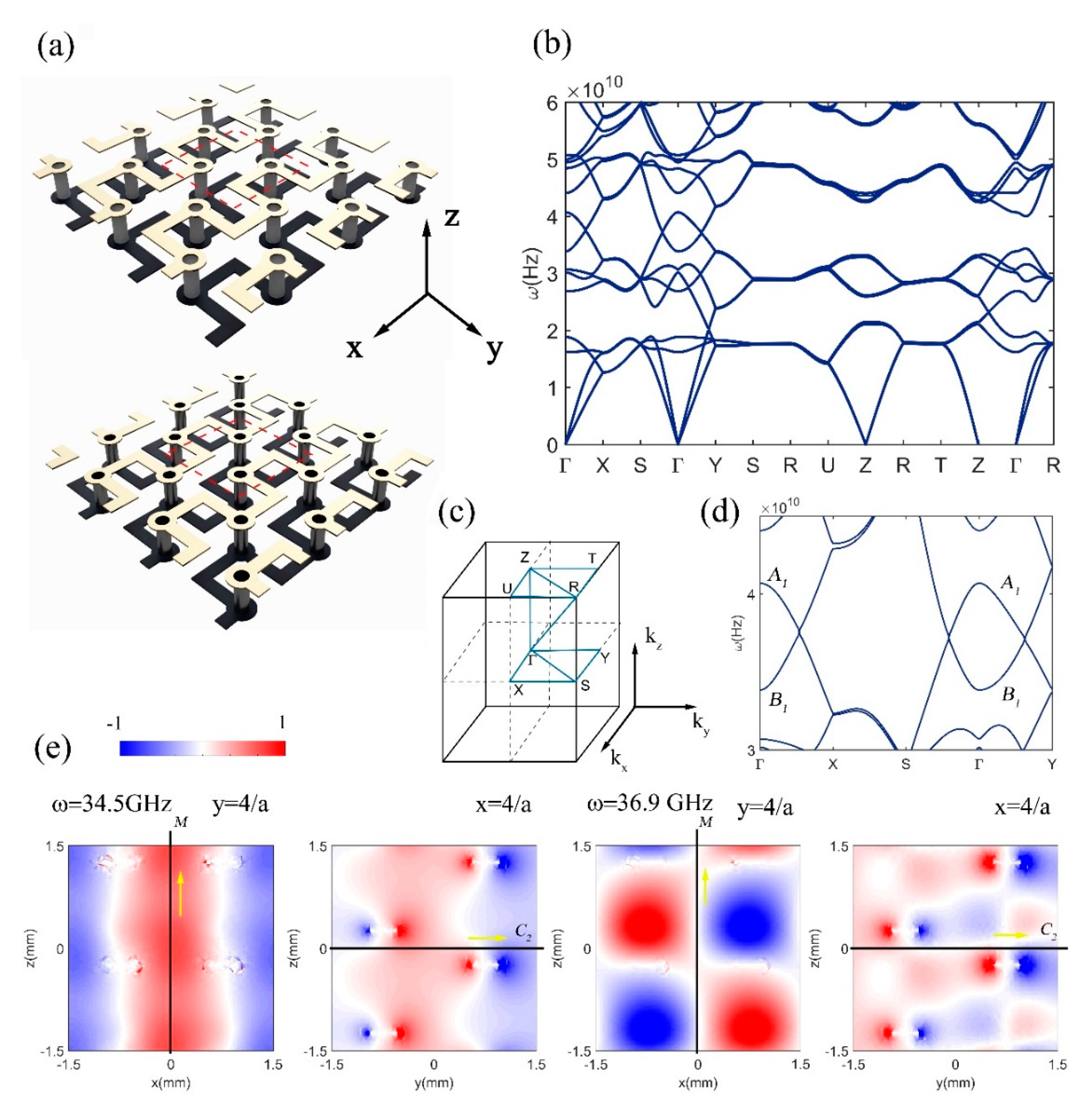
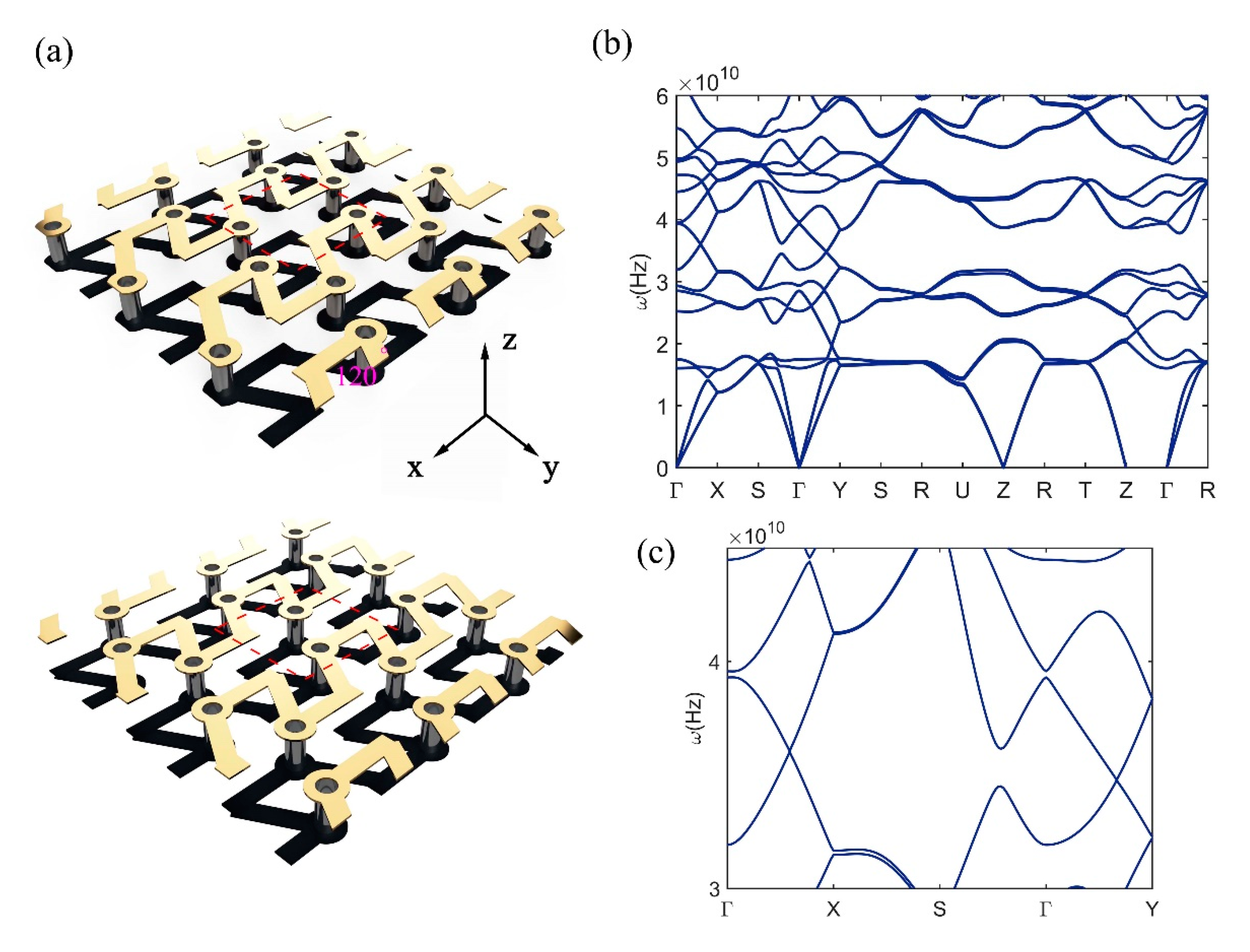
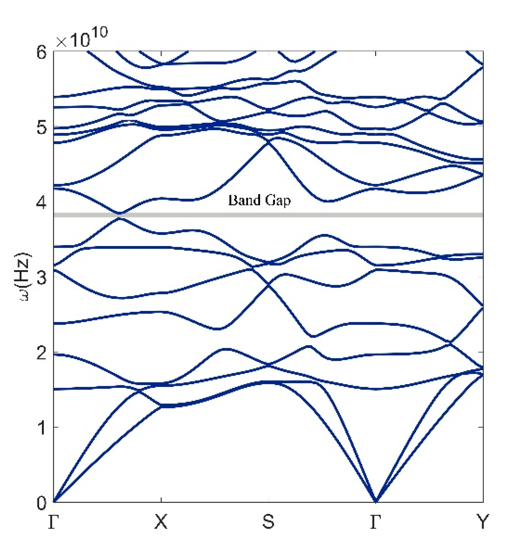
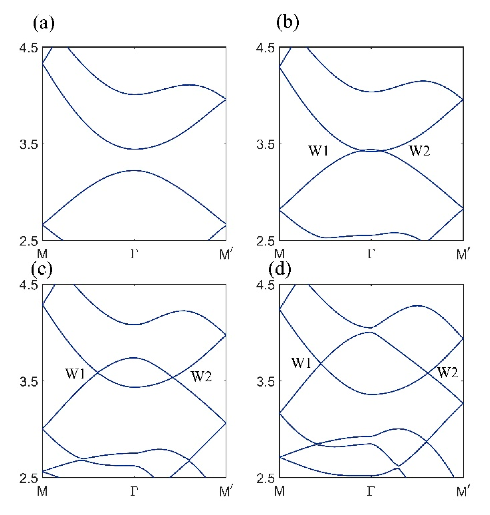
2.1. Line Node from SG 61

Without the deformation, the metacrystal structure belongs to SG 61, whose group representatives are translational symmetry T, three glide symmetries G x , y , z , three screw rotation symmetries S 2 , x , y , z , and inversion symmetry P. The nonsymmorphic group operations are expressed explicitly as:
G x ( x , y , z ) ( x , y , z + 1 2 )
G y ( x , y , z ) ( x + 1 2 , y , z )
G z ( x , y , z ) ( x , y + 1 2 , z )
S 2 x ( x , y , z ) ( x + 1 2 , y , z + 1 2 )
S 2 y ( x , y , z ) ( x , y + 1 2 , z )
S 2 z ( x , y , z ) ( x + 1 2 , y , z + 1 2 )
Nonsymmorphic group operations have been extensively used to protect degeneracies at the boundaries of the Brillouin zone beyond the capabilities of point group [43,44]. A band diagram of the metacrystal is given in Figure 1b, whose sweeping path is given in Figure 1c, and presents band crossings along the high symmetry lines Γ X S Γ and Γ Y that is line node (LN) degeneracy. Noticeably, the band diagram is pseudo-gapped for the LN, meaning no other excessive bands can be found around the LN frequency at other sites in the Brillouin zone. Furthermore, on the edge of the Brillouin zone (RS, RU and RT high symmetry lines), Dirac nodal lines are found, featuring four-fold degeneracy on the whole edges [45].

2.2. Group Theory Analysis

Since the LN is due to an accidental degeneracy that resides on the high symmetry line/plane, the two bands consisting of LN degeneracy are expected to belong to different irreducible group representations. On the high symmetry lines Γ X and Γ Y , the little group reduced to G Γ X = { E ,   S 2 y ,   G x ,   G z , T } and G Γ Y = { E ,   S 2 x ,   G y ,   G z , T }, respectively. Despite the existence of the half unit cell translations within the nonsymmorphic operations, the coset groups G Γ X / T ,   G Γ Y / T of the little groups are found to be isomorphic to simple point group C 2 v , whose character and compatability tables are given below in Table 1 and Table 2. Note that on the Γ X and Γ Y high symmetry lines, the σ v mirror operation are σ y and σ x while σ v is σ z .
Field distributions of the electrical component e x = E x e i k r on the momentums half way on Γ X and Γ Y are given in Figure 1e. Note that after multiplying the phase factor e i k r , e x is the periodic function in the primitive cell. The left two and the right two images belong to the same frequency, respectively. In the figures, the mirror plane and the rotation axis are illustrated by the solid black lines, and the half unit cell translations related to the nonsymmorphic group operations are illustrated by the yellow arrow. In the left two figures in Figure 1e, it can be inspected that the state is an even state under the glide operation, and an odd state under the screw rotation operation from their (0 1 0) and (1 0 0) direction’s fields. The group representation is, thus, B 1 according to Table 1. Whereas, for the other state consisting the LN, it is odd under the glide operation and even under the screw rotation operation, meaning the group representation is A 1 .

2.3. Weyl Point from SG 19

What the group theory analysis can show is that after introducing certain structure deformation, whether the band crossing is kept or gapped can be predicted. Introducing the deformation shown in Figure 2a will essentially reduce the original SG 61 to SG 19, since the only remaining symmetries are the three screw rotations. Therefore, on the Γ X and Γ Y high symmetry lines, the little groups are isomorphic to point group C 2 (Table 2). In the compatibility relation in Table 2, A 1 and B 1 can be reduced to different irreducible representations A and B , meaning the band crossings are kept, while gapped when k is away from the high symmetry lines.
Instead, if the original metacrystal is reduced to SG 29 by keeping S x , y and G z , the isomorphic point group is C v in the compatibility relation in Table 2. The irreducible representations are A for both the bands, meaning the LN is immediately gapped. This is consistent with the fact that Weyl nodes cannot be found on mirror planes since mirror operations can flip the chirality of the Weyl nodes. The band structure of the SG 29 metacrystal is given in Figure 3, showing a full band gap around 36 GHz.

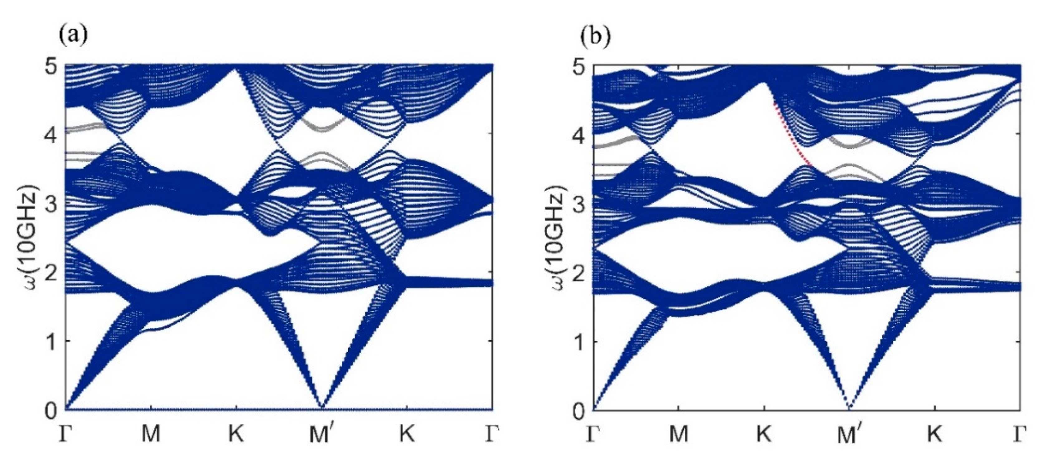
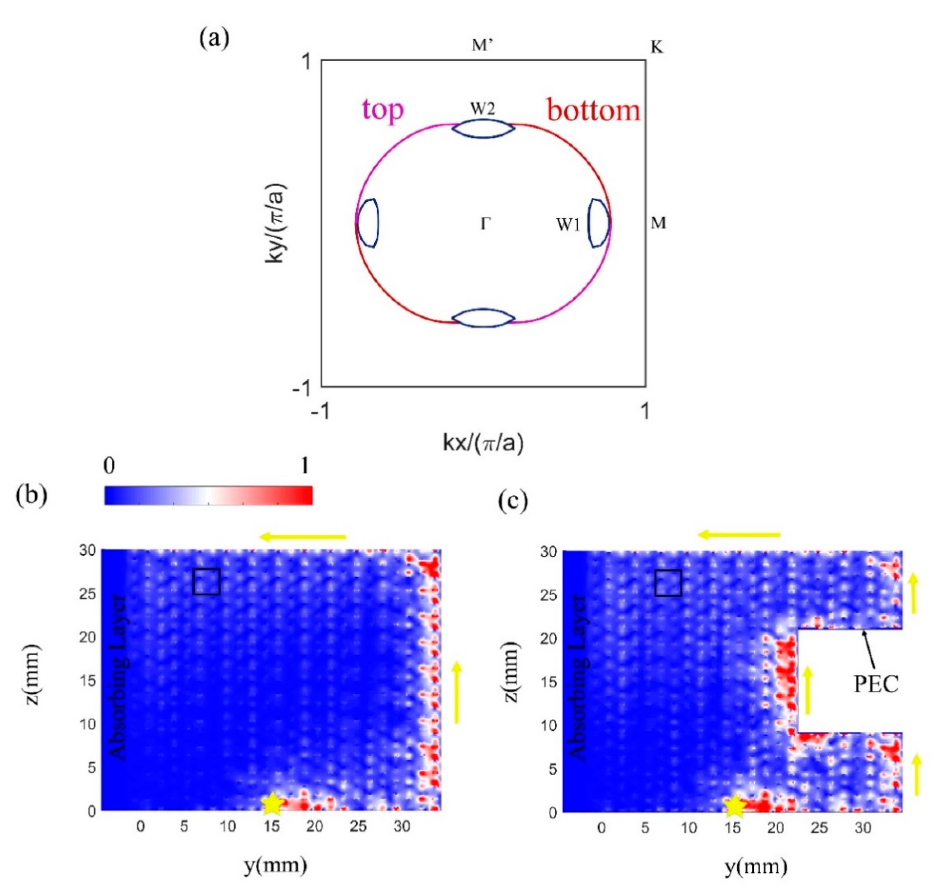
2.4. Surface States of the LN and the WN

It has been well understood that LN and WN hold surface states. LN hold the ‘drumhead’ surface states and are normally flat bands that could enhance interactions and are promising for high temperature superconductivity. The WN, on the other hand, hold the so-called Fermi arcs that have been exploited in their intriguing transport properties and unconventional quantum Hall effects [14].
To explore the surface states of the metacrystal, we created super cell configurations that are periodic in the x and y direction and are confined with perfect electrical conductors (PEC) with 10 unit cells in the z-direction. The results are illustrated in Figure 4 and the configuration of the projected surface Brillouin is give in Figure 5. For the unperturbed LN metacrystal, surface states that are reminiscences of the drumhead surface states are found, while for the WN metacrystal, Fermi arcs are found around the momentums where LN are found (red dots in Figure 4b).
At a fixed frequency (36.5 GHz in Figure 5), Fermi arcs are found to connect WN with opposite Chern numbers (WN1 and WN2 located on the kx and ky axis, respectively), which are the results of the integral of Berry curvatures on a closed surface that include a WN [1]. The Fermi arcs are illustrated by the magenta and red lines that are residing on the top and the bottom surfaces, respectively. Figure 5b shows the real space field distribution of the topological surface state excited by a line current source that fixes the k x at 0.2 π / a . The unidirectionality of the surface state propagation is consistent to the calculated equi-frequency contour in Figure 5a. Figure 5c shows the same surface state excitation simulation with an extra square-shaped defect. Again, the unidirectionality demonstrates the topological robustness of the fermi arc surfaces.

3. Discussion

Our design has shown how to obtain WN in SG 19 from LN in SG 61. The pure PCB layered design could also benefit the tunings of the WN. In Figure 6, we show the band diagrams of the WN metacrystal with various z-direction periods. Note that the PCB layers’ thicknesses are conserved at 1 mm and only the interlayer dielectric boards’ thickness is changed. Intriguingly, locations of the WN in the Brillouin zone can be effectively tuned by the periodicity. Note that when the thickness is reduced to below 4.8 mm, the WN coalesce and annihilate. The highly sensitive locations of the WN to the periodicity could be used to generate giant effective magnetic fields in the WN metacrystal by introducing a gradually changing thickness. Since photons do not respond to actual magnetic fields, effective magnetic fields are crucial for mimicking the physical effects of real magnetic fields, for example, Landau quantization and chiral zero modes [46,47].

Author Contributions

Conceptualization, W.G. and Y.-T.W.; software, W.G.; validation, W.G. and Y.-T.W.; formal analysis, W.G. and Y.-T.W.; writing—original draft preparation, W.G.; writing—review and editing, W.G. and Y.-T.W.; supervision, W.G. and Y.-T.W. All authors have read and agreed to the published version of the manuscript.

Funding

This project has received funding from the European Research Council (ERC) under the European Union’s Horizon 2020 research and innovation programme (grant agreement No 724306); Engineering and Physical Science Research Council (EP/T002654/1); Leverhulme Trust (Topologically protected flexural waves in thin elastic plates).

Conflicts of Interest

The authors declare no conflict of interest.

References

  1. Wan, X.; Turner, A.M.; Vishwanath, A.; Savrasov, S.Y. Topological semimetal and Fermi-arc surface states in the electronic structure of pyrochlore iridates. Phys. Rev. B 2011, 83, 205101. [Google Scholar] [CrossRef] [Green Version]
  2. Burkov, A.A.; Balents, L. Weyl semimetal in a topological insulator multilayer. Phys. Rev. Lett. 2011, 107, 127205. [Google Scholar] [CrossRef] [PubMed] [Green Version]
  3. Armitage, N.P.; Mele, E.J.; Vishwanath, A. Weyl and Dirac semimetals in three-dimensional solids. Rev. Mod. Phys. 2018, 90, 015001. [Google Scholar] [CrossRef] [Green Version]
  4. Huang, X.; Zhao, L.; Long, Y.; Wang, P.; Chen, D.; Yang, Z.; Liang, H.; Xue, M.; Weng, H.; Fang, Z.; et al. Observation of the chiral-anomaly-induced negative magnetoresistance: In 3D Weyl semimetal TaAs. Phys. Rev. X 2015, 5, 031023. [Google Scholar] [CrossRef] [Green Version]
  5. Li, Q.; Kharzeev, D.E.; Zhang, C.; Huang, Y.; Pletikosić, I.; Fedorov, A.V.; Zhong, R.D.; Schneeloch, J.A.; Gu, G.D.; Valla, T. Chiral magnetic effect in ZrTe5. Nat. Phys. 2016, 12, 550–554. [Google Scholar] [CrossRef] [Green Version]
  6. Xiong, J.; Kushwaha, S.K.; Liang, T.; Krizan, J.W.; Hirschberger, M.; Wang, W.; Cava, R.J.; Ong, N.P. Evidence for the chiral anomaly in the Dirac semimetal Na3Bi. Science 2015, 350, 413–416. [Google Scholar] [CrossRef] [Green Version]
  7. Fang, C.; Lu, L.; Liu, J.; Fu, L. Topological semimetals with helicoid surface states. Nat. Phys. 2016, 12, 936–941. [Google Scholar] [CrossRef]
  8. Xu, S.-Y.; Belopolski, I.; Sanchez, D.S.; Guo, C.; Chang, G.; Zhang, C.; Bian, G.; Yuan, Z.; Lu, H.; Feng, Y.; et al. Experimental discovery of a topological Weyl semimetal state in TaP. Sci. Adv. 2015, 1, e1501092. [Google Scholar] [CrossRef] [Green Version]
  9. Lv, B.Q.; Xu, N.; Weng, H.M.; Ma, J.Z.; Richard, P.; Huang, X.C.; Zhao, L.X.; Chen, G.F.; Matt, C.E.; Bisti, F.; et al. Observation of Weyl nodes in TaAs. Nat. Phys. 2015, 11, 724–727. [Google Scholar] [CrossRef]
  10. Weng, H.; Fang, C.; Fang, Z.; Andrei Bernevig, B.; Dai, X. Weyl semimetal phase in noncentrosymmetric transition-metal monophosphides. Phys. Rev. X 2015, 5, 011029. [Google Scholar] [CrossRef]
  11. Yang, L.X.; Liu, Z.K.; Sun, Y.; Peng, H.; Yang, H.F.; Zhang, T.; Zhou, B.; Zhang, Y.; Guo, Y.F.; Rahn, M.; et al. Weyl semimetal phase in the non-centrosymmetric compound TaAs. Nat. Phys. 2015, 11, 728–732. [Google Scholar] [CrossRef] [Green Version]
  12. Hasan, M.Z.; Xu, S.-Y.; Belopolski, I.; Huang, S.-M. Discovery of Weyl fermion semimetals and topological Fermi arc states. Annu. Rev. Condens. Matter Phys. 2017, 8, 289–309. [Google Scholar]
  13. Sanchez, D.S.; Belopolski, I.; Cochran, T.A.; Xu, X.; Yin, J.X.; Chang, G.; Xie, W.; Manna, K.; Süß, V.; Huang, C.Y.; et al. Topological chiral crystals with helicoid-arc quantum states. Nature 2019, 567, 500–505. [Google Scholar] [CrossRef]
  14. Wang, C.M.; Sun, H.P.; Lu, H.Z.; Xie, X.C. 3D Quantum Hall Effect of Fermi Arc in Topological Semimetals. Phys. Rev. Lett. 2017, 119, 136806. [Google Scholar] [CrossRef] [PubMed] [Green Version]
  15. Deng, K.; Wan, G.; Deng, P.; Zhang, K.; Ding, S.; Wang, E.; Yan, M.; Huang, H.; Zhang, H.; Xu, Z.; et al. Experimental observation of topological Fermi arcs in type-II Weyl semimetal MoTe2. Nat. Phys. 2016, 12, 1105–1110. [Google Scholar] [CrossRef]
  16. Burkov, A.A. Anomalous hall effect in weyl metals. Phys. Rev. Lett. 2014, 113, 187202. [Google Scholar] [CrossRef] [Green Version]
  17. Sodemann, I.; Fu, L. Quantum Nonlinear Hall Effect Induced by Berry Curvature Dipole in Time-Reversal Invariant Materials. Phys. Rev. Lett. 2015, 115, 216806. [Google Scholar] [CrossRef] [Green Version]
  18. Ma, Q.; Xu, S.Y.; Shen, H.; MacNeill, D.; Fatemi, V.; Chang, T.R.; Mier Valdivia, A.M.; Wu, S.; Du, Z.; Hsu, C.H.; et al. Observation of the nonlinear Hall effect under time-reversal-symmetric conditions. Nature 2019, 565, 337–342. [Google Scholar] [CrossRef] [Green Version]
  19. Bradlyn, B.; Cano, J.; Wang, Z.; Vergniory, M.G.; Felser, C.; Cava, R.J.; Bernevig, B.A. Beyond Dirac and Weyl fermions: Unconventional quasiparticles in conventional crystals. Science 2016, 353, aaf5037. [Google Scholar] [CrossRef] [Green Version]
  20. Yang, B.J.; Nagaosa, N. Classification of stable three-dimensional Dirac semimetals with nontrivial topology. Nat. Commun. 2014, 5, 1–10. [Google Scholar] [CrossRef] [Green Version]
  21. Hu, J.; Tang, Z.; Liu, J.; Liu, X.; Zhu, Y.; Graf, D.; Myhro, K.; Tran, S.; Lau, C.N.; Wei, J.; et al. Evidence of Topological Nodal-Line Fermions in ZrSiSe and ZrSiTe. Phys. Rev. Lett. 2016, 117, 016602. [Google Scholar] [CrossRef] [Green Version]
  22. Gibson, Q.D.; Schoop, L.M.; Muechler, L.; Xie, L.S.; Hirschberger, M.; Ong, N.P.; Car, R.; Cava, R.J. Three-dimensional Dirac semimetals: Design principles and predictions of new materials. Phys. Rev. B 2015, 91, 205128. [Google Scholar] [CrossRef] [Green Version]
  23. Young, S.M.; Zaheer, S.; Teo JC, Y.; Kane, C.L.; Mele, E.J.; Rappe, A.M. Dirac semimetal in three dimensions. Phys. Rev. Lett. 2012, 108, 140405. [Google Scholar] [CrossRef] [PubMed]
  24. Neupane, M.; Xu, S.Y.; Sankar, R.; Alidoust, N.; Bian, G.; Liu, C.; Belopolski, I.; Chang, T.R.; Jeng, H.T.; Lin, H.; et al. Observation of a three-dimensional topological dirac semimetal phase in high-mobility cd3 as2. Nat. Commun. 2014, 5, 1–8. [Google Scholar] [CrossRef] [PubMed] [Green Version]
  25. Wang, Z.; Weng, H.; Wu, Q.; Dai, X.; Fang, Z. Three-dimensional Dirac semimetal and quantum transport in Cd 3As2. Phys. Rev. B 2013, 88, 125427. [Google Scholar] [CrossRef] [Green Version]
  26. Borisenko, S.; Gibson, Q.; Evtushinsky, D.; Zabolotnyy, V.; Büchner, B.; Cava, R.J. Experimental realization of a three-dimensional dirac semimetal. Phys. Rev. Lett. 2014, 113, 027603. [Google Scholar] [CrossRef] [Green Version]
  27. Chang, G.; Xu, S.Y.; Wieder, B.J.; Sanchez, D.S.; Huang, S.M.; Belopolski, I.; Chang, T.R.; Zhang, S.; Bansil, A.; Lin, H.; et al. Unconventional Chiral Fermions and Large Topological Fermi Arcs in RhSi. Phys. Rev. Lett. 2017, 119, 206401. [Google Scholar] [CrossRef] [Green Version]
  28. Wang, R.; Xia, B.W.; Chen, Z.J.; Zheng, B.B.; Zhao, Y.J.; Xu, H. Symmetry-Protected Topological Triangular Weyl Complex. Phys. Rev. Lett. 2020, 124, 105303. [Google Scholar] [CrossRef] [Green Version]
  29. Tang, P.; Zhou, Q.; Zhang, S.C. Multiple Types of Topological Fermions in Transition Metal Silicides. Phys. Rev. Lett. 2017, 119, 206402. [Google Scholar] [CrossRef] [Green Version]
  30. Zhang, T.; Song, Z.; Alexandradinata, A.; Weng, H.; Fang, C.; Lu, L.; Fang, Z. Double-Weyl Phonons in Transition-Metal Monosilicides. Phys. Rev. Lett. 2018, 120, 016401. [Google Scholar] [CrossRef] [Green Version]
  31. Lu, L.; Wang, Z.; Ye, D.; Ran, L.; Fu, L.; Joannopoulos, J.D.; Soljačić, M. Experimental observation of Weyl points. Science 2015, 349, 622–624. [Google Scholar] [CrossRef] [PubMed] [Green Version]
  32. Lu, L.; Fu, L.; Joannopoulos, J.D.; Soljacic, M. Weyl points and line nodes in gyroid photonic crystals. Nat. Photonics 2013, 7, 294. [Google Scholar] [CrossRef] [Green Version]
  33. Chang, M.L.; Xiao, M.; Chen, W.J.; Chan, C.T. Multiple Weyl points and the sign change of their topological charges in woodpile photonic crystals. Phys. Rev. B. 2017, 95, 125136. [Google Scholar] [CrossRef] [Green Version]
  34. Chen, W.J.; Xiao, M.; Chan, C.T. Photonic crystals possessing multiple Weyl points and the experimental observation of robust surface states. Nat. Commun. 2016, 7, 1–10. [Google Scholar] [CrossRef] [PubMed]
  35. Yang, B.; Guo, Q.; Tremain, B.; Liu, R.; Barr, L.E.; Yan, Q.; Gao, W.; Liu, H.; Xiang, Y.; Chen, J.; et al. Ideal Weyl points and helicoid surface states in artificial photonic crystal structures. Science 2018, 359, 1013–1016. [Google Scholar] [CrossRef] [Green Version]
  36. Yang, B.; Guo, Q.; Tremain, B.; Barr, L.E.; Gao, W.; Liu, H.; Béri, B.; Xiang, Y.; Fan Di Hibbins, A.P.; Zhang, S. Direct observation of topological surface-state arcs in photonic metamaterials. Nat. Commun. 2017, 8, 1–7. [Google Scholar] [CrossRef] [Green Version]
  37. Xiao, M.; Lin, Q.; Fan, S. Hyperbolic Weyl Point in Reciprocal Chiral Metamaterials. Phys. Rev. Lett. 2016, 117, 057401. [Google Scholar] [CrossRef] [Green Version]
  38. Gao, W.; Yang, B.; Lawrence, M.; Fang, F.; Béri, B.; Zhang, S. Photonic Weyl degeneracies in magnetized plasma. Nat. Commun. 2016, 7, 1–8. [Google Scholar] [CrossRef] [Green Version]
  39. Wang, D.; Yang, B.; Gao, W.; Jia, H.; Yang, Q.; Chen, X.; Wei, M.; Liu, C.; Navarro-Cía, M.; Han, J.; et al. Photonic Weyl points due to broken time-reversal symmetry in magnetized semiconductor. Nat. Phys. 2019, 15, 1150–1155. [Google Scholar] [CrossRef]
  40. Lin, Q.; Xiao, M.; Yuan, L.; Fan, S. Photonic Weyl point in a two-dimensional resonator lattice with a synthetic frequency dimension. Nat. Commun. 2016, 7, 1–7. [Google Scholar] [CrossRef] [Green Version]
  41. Wang, Q.; Xiao, M.; Liu, H.; Zhu, S.; Chan, C.T. Optical interface states protected by synthetic weyl points. Phys. Rev. X 2017, 7, 031032. [Google Scholar] [CrossRef]
  42. Ruan, J.; Jian, S.K.; Yao, H.; Zhang, H.; Zhang, S.C.; Xing, D. Symmetry-protected ideal Weyl semimetal in HgTe-class materials. Nat. Commun. 2016, 7, 1–6. [Google Scholar] [CrossRef] [PubMed]
  43. Wang, S.S.; Liu, Y.; Yu, Z.M.; Sheng, X.L.; Yang, S.A. Hourglass Dirac chain metal in rhenium dioxide. Nat. Commun. 2017, 8, 1–7. [Google Scholar] [CrossRef] [PubMed] [Green Version]
  44. Young, S.M.; Kane, C.L. Dirac Semimetals in Two Dimensions. Phys. Rev. Lett. 2015, 115, 126803. [Google Scholar] [CrossRef] [Green Version]
  45. Li, S.; Liu, Y.; Wang, S.S.; Yu, Z.M.; Guan, S.; Sheng, X.L.; Yao, Y.; Yang, S.A. Nonsymmorphic-symmetry-protected hourglass Dirac loop, nodal line, and Dirac point in bulk and monolayer X3SiTe6 (X = Ta, Nb). Phys. Rev. B 2018, 97, 045131. [Google Scholar] [CrossRef] [Green Version]
  46. Fang, K.; Yu, Z.; Fan, S. Realizing effective magnetic field for photons by controlling the phase of dynamic modulation. Nat. Photonics. 2012, 6, 782–787. [Google Scholar] [CrossRef]
  47. Jia, H.; Zhang, R.; Gao, W.; Guo, Q.; Yang, B.; Hu, J.; Bi, Y.; Xiang, Y.; Liu, C.; Zhang, S. Observation of chiral zero mode in inhomogeneous three-dimensional Weyl metamaterials. Science 2019, 363, 148–151. [Google Scholar] [CrossRef] [Green Version]
Figure 1. (a) First and second layer structure of the line node metacrystal. (b) Band diagram of the line node structure. (c) Detailed band diagram of the line node. (d) Brillouin zone and the path for band diagram. (e) E x field components of the line nodes eigen modes found at k y = π 2 a   ,   k x = 0 ,   k z = 0 and the frequency ω at 34.5 and 36.9 GHz, respectively.
Crystals 10 00605 g001
Figure 2. (a) First and second layer of the perturbed metacrystal structure. (b) Band diagram of the perturbed metacrystal. (c) Detailed band diagram of the metacrystal around the Weyl node frequency. The Weyl nodes are found on the Γ X and Γ Y high symmetry lines, and the band crossings at other momentums are gapped.
Crystals 10 00605 g002
Figure 3. Band structure of the SG 29 metacrystal.
Crystals 10 00605 g003
Figure 4. (a) Surface states (gray) and projected bulk band structure of the line node metacrystal in SG 61. (b) Surface states (gray/red) and projected bulk band structure of the line node metacrystal in SG 61; the topological Fermi arcs connecting the Weyl nodes are in red.
Crystals 10 00605 g004
Figure 5. (a) Equi-frequency contour of the projected Weyl nodes and the Fermi arcs. Red and Magenta lines are on the top and bottom surface, respectively. (b,c) Excitation of topological fermi arc surface states with and without a square-shaped defect. Source is an x direction line current fixing the k x at 0.2 π / a , marked by the yellow pentagram. The metacrystals are bounded by the perfect electric conductor (PEC) boundary condition. The unit cell is outlined by the solid black line box.
Crystals 10 00605 g005
Figure 6. Band diagrams of the Weyl node for various unit cell z-direction periods. (a) The Weyl nodes coalesce and annihilate at 4.6 mm. (b) Weyl nodes are in the proximity of Γ point in the Brillouin zone at 4.8 mm. (c,d) Weyl node at 5 and 5.5 mm period.
Crystals 10 00605 g006
Table 1. Character table of group C 2 v .
C 2 v E C 2 σ v σ v
A 1 1111
A 2 11−1−1
B 1 1−11−1
B 2 1−1−11
Table 2. Compatibility table of group C 2 v .
C 2 v C 2 C v C v
A 1 A A A
A 2 A A A
B 1 B A A
B 2 B A A

