Article

Initial Growth and Crystallization Onset of Plasma Enhanced-Atomic Layer Deposited ZnO

1
Institute of Solid State Physics, NAWI Graz, Graz University of Technology, Petersgasse 16, 8010 Graz, Austria
2
Institute of Pharmaceutical Sciences, Department of Pharmaceutical Technology, University of Graz, 8010 Graz, Austria
*
Author to whom correspondence should be addressed.
The authors A. P. and J. P. share the first authorship.
Crystals 2020, 10(4), 291; https://doi.org/10.3390/cryst10040291
Submission received: 24 March 2020 / Revised: 7 April 2020 / Accepted: 8 April 2020 / Published: 10 April 2020
(This article belongs to the Special Issue Functional Oxide Based Thin-Film Materials (Volume II))

Abstract

:
Direct plasma enhanced-atomic layer deposition (PE-ALD) is adopted for the growth of ZnO on c-Si with native oxide at room temperature. The initial stages of growth both in terms of thickness evolution and crystallization onset are followed ex-situ by a combination of spectroscopic ellipsometry and X-ray based techniques (diffraction, reflectivity, and fluorescence). Differently from the growth mode usually reported for thermal ALD ZnO (i.e., substrate-inhibited island growth), the effect of plasma surface activation resulted in a substrate-enhanced island growth. A transient region of accelerated island formation was found within the first 2 nm of deposition, resulting in the growth of amorphous ZnO as witnessed with grazing incidence X-ray diffraction. After the islands coalesced and a continuous layer formed, the first crystallites were found to grow, starting the layer-by-layer growth mode. High-temperature ALD ZnO layers were also investigated in terms of crystallization onset, showing that layers are amorphous up to a thickness of 3 nm, irrespective of the deposition temperature and growth orientation.

1. Introduction

Zinc oxide (ZnO) is a II-VI semiconductor, well-studied because of its unique qualities. As thin films, it has been researched for an increasing number of optical and electronic devices, and the tunability of its physical-chemical properties is still investigated in various scientific fields [1,2,3,4]. To name a few, it possesses a wide direct bandgap (~3.37 eV) and large excitonic binding energy (~60 meV), which is useful for near-UV optoelectronics and lasing applications [5,6]. Furthermore, it is applied as a transparent conductive oxide due to the possibility to tune its electrical properties via doping, e.g., aluminum doping [7,8].
Several vapor phase methods are adopted for the deposition of ZnO thin films, such as sputtering [9], pulsed laser deposition [10], and atomic layer deposition (ALD). ALD, either thermal or enhanced by plasma (PE-ALD), has often been adopted as the method of choice to deliver high quality (ultra-)thin ZnO films [4,11,12,13,14,15,16]. Polycrystalline thin films were obtained down to room temperature [4,17,18]. PE-ALD is known to deliver ZnO of higher quality compared to thermal ALD, with a fewer number of defects (e.g., oxygen vacancies and Zn interstitials) and a higher mass density, both at room and elevated temperatures [4,11,19,20]. The highly reactive species formed in the plasma phase are considered the key aspect for the improved material quality, contributing to a more efficient removal of the organic ligands in the ALD Zn-organometallic precursor, and generally an improved crystallogenic packing [21,22].
Recently in the literature, great attention has been given to the initial stages of growth of ZnO by thermal ALD [23,24,25,26,27,28,29,30]. Understanding the first stages of growth is of particular importance when ultrathin and continuous ZnO films are required, e.g., as an electron buffer layer for inverted solar cells [4], or as a passivation layer in transistors [31,32]. Depending on the temperature and substrate material adopted, the growth was found to be from island-like to layer-by-layer or epitaxial, highlighting the great influence of these parameters in the growth stages. Following the growth mode schemes presented by Puruunen and Vandervorst [33], ZnO grown by ALD generally showed a substrate-inhibited growth.
Together with the initial growth, the onset of crystallization represents another critical aspect when the first stages of the deposition of materials are investigated. The first crystalline units could develop as early as the first atomic layer or in a later stage of deposition and the details can depend on the growth orientation, interaction with the substrate and/or the adopted method (e.g., if thermal or plasma enhanced-ALD) [22]. Compared to the initial growth stages, the onset of crystallinity has not received the same attention. In a series of investigations on thermal ALD ZnO, Renevier, Ciatto et al. reported on the growth of ZnO when deposited on different substrates (a-SiO2 [26,27,28], c-Al2O3 [26,27,28], In0.53Ga0.47As [29,30]). The in-situ methodology adopted (mainly X-ray based methods, such as X-ray fluorescence and X-ray absorption near-edge structure spectroscopy) identified the onset of crystallization to start from the very first cycle when deposited on c-Al2O3, adopting a 2D-like growth and developing in-plane crystallinity; a different growth behavior was instead observed when deposited on a-SiO2 and In0.53Ga0.47As, on which the crystallinity starts after the development of an initial amorphous layer.
In this contribution, the initial growth and onset of crystallization of ZnO is investigated by adopting a direct plasma-enhanced ALD (PE-ALD) approach, thus highlighting the role of plasma surface activation. The initial stages of growth of inorganic materials have been seldom investigated for PE-ALD, [34,35,36] and the specific nucleation of crystallites adopting plasma as co-reactant has not been reported for ZnO. Following the studies on room [18] and high temperature deposition of ZnO by direct PE-ALD, the evolution of the material properties is investigated with a combination of several ex-situ analysis techniques.

2. Experimental

A custom-built direct plasma ALD reactor was used to deposit ZnO thin films on single side polished c-Si (100) substrates (Siegert Wafer, Aachen, Germany) with native oxide. Details on the system can be found in previous publications [18,37,38,39]. The pressure in the reactor was controlled via a manual gate valve, set to a fixed opening to reach a pressure of around 85 mTorr during plasma exposure. Pure oxygen was used during the plasma step (step A, plasma power 60 W, duration 6 s for O2 exposure) and Ar was adopted in the purging step. The flow rates for O2 and Ar were set at 20 sccm during the plasma and the purging step, respectively. Diethyl zinc (DEZ, Sigma-Aldrich, Darmstadt, Germany, CAS 557-20-0) was used as the metalorganic precursor (step B, duration 150 ms). The purging times were set at 12 s and 15 s for step A and B, respectively. The cycles always started and ended with a plasma step, as follows: (A-B)n-A, with n the number of cycles. The last plasma step was adopted to ensure the removal of the organic ligands of DEZ also on the surface of the layer. Sets of samples were deposited at constant temperatures in the range from 25 to 250 °C [39]. Thickness variation of the films was achieved by varying the number of cycles.
Spectroscopic ellipsometry (SE) (J.A. Woollam M-2000V, Lincoln, NE, USA) was used to determine the thickness and optical properties of the films after deposition. The measurements were carried out at three different angles (65°, 70°, and 75°) in a wavelength range from 370 to 1000 nm. The analysis of the spectra was performed with the software CompleteEASE® (J.A. Woollam, Lincoln, NE, USA). The thickness was determined by applying a three-layer model consisting of a semi-infinite silicon substrate, a native silicon oxide layer with a fixed thickness of 1.3 to 2 nm (measured before each deposition), and a Cauchy layer, as follows
n λ = A + B λ 2 + C λ 4
where n is the wavelength-dependent refractive index, λ is the wavelength and A, B, and C are fit parameters. The fitting was limited to the transparent region of ZnO, i.e., 450–1000 nm.
To verify the robustness of the model adopted, the analysis was extended to a wavelength range close to the bandgap of ZnO (generally reported at 375 nm). An oscillator model was also adopted, extending the wavelength range to 370 to 1000 nm. The oscillator model consisted of Gaussian oscillators to account for the high- and near infrared-energy contributions and a PSEMI-M0 model to account for the near-bandgap absorption. The PSEMI-M0 model is an oscillator with a sharp onset and Kramers–Kronig consistent properties consisting of four connected polynomial spline functions [40]. The two models were found to deliver comparable results for the thickness investigated, and thus, the Cauchy model was preferred due to the lower number of variables adopted.
As a complementary technique to ellipsometry, X-ray reflectivity (XRR) measurements were performed to determine the film thickness and density as well as the surface and interface roughness. A PANalytical Empyrean diffractometer (Malvern Panalytical, Kassel, Germany) utilizing monochromatized copper radiation with a wavelength λ = 1.5418 Å was used. The beam was narrowed by a 1/32° divergence slit and a 10 mm beam mask. Its PIXcel3D-detector was operated in receiving slit mode, facilitating the P 0.1 antiscatter slit. Two different fitting procedures were applied to explain the experimental data: a model-dependent and a model-independent approach. For the first, fitting of the measured data was performed with the software X’Pert Reflectivity (Panalytical, The Netherlands) applying a three-layer model consisting of a semi-infinite Si substrate, a native SiO2 layer, and a ZnO layer. The fit parameters in the model were the ZnO layer thickness, density, and surface roughness as well as the interface roughness with the native SiO2 layer on the c-Si. The approach here used a segmented algorithm to fit the model onto the experimental data. The second fitting method is a stochastic model-independent electron density profiles variation using the software Stochfit [41]. A scattering length density (SLD) of 19.5 was chosen for the subphase (SiO2) and the initial value for the film SLD was 40. For sake of simplicity, the initial value for the film thickness was the one obtained by the other fit using the X’Pert Reflectivity software and the number of boxes was 1.5 times this value.
Grazing incidence X-ray diffraction (GIXD) was performed on the thin films of ZnO to investigate the in-plane orientation of the crystallites with respect to the silicon oxide surface. The measurements were conducted at the synchrotron Elettra (Trieste, Italy) using the XRD1-beamline [42]. The wavelength was set at 1.4 Å and an incident angle α of 1.2 to 2° was chosen to minimize footprint artifacts. Diffracted intensities were collected on a Pilatus 2M detector and all data have been recalculated to reciprocal space maps using the in-house developed software package GIDVis [43].
X-ray fluorescence (XRF) spectroscopy was performed with an PANalytical Epsilon 1 (Malvern Panalytical, Kassel, Germany) to obtain the relative Zn amount after different deposition steps. X-rays were generated in an Ag anode X-ray tube using a voltage and current of 50 kV and 100 µA, respectively. A 100 µm Ag-filter was used in the measurements, and the intensity of the Zn-Kα peak at 8.63 keV was evaluated.
Atomic force microscopy (AFM) was performed in non-contact mode on a Nanosurf Easyscan 2 (Liestal, Switzerland) equipped with a C3000 controller. The tapping mode measurements were performed using a TAP-300 cantilever (BudgetSensors, Bulgaria). The correction of artifacts, plotting, and data evaluation were done with the freely available software package Gwyddion [44]. The samples were rinsed with water and 96% EtOH and dried for 5 minutes on a hot plate at 60 °C under constant nitrogen stream to obtain high quality images.

3. Results and Discussion

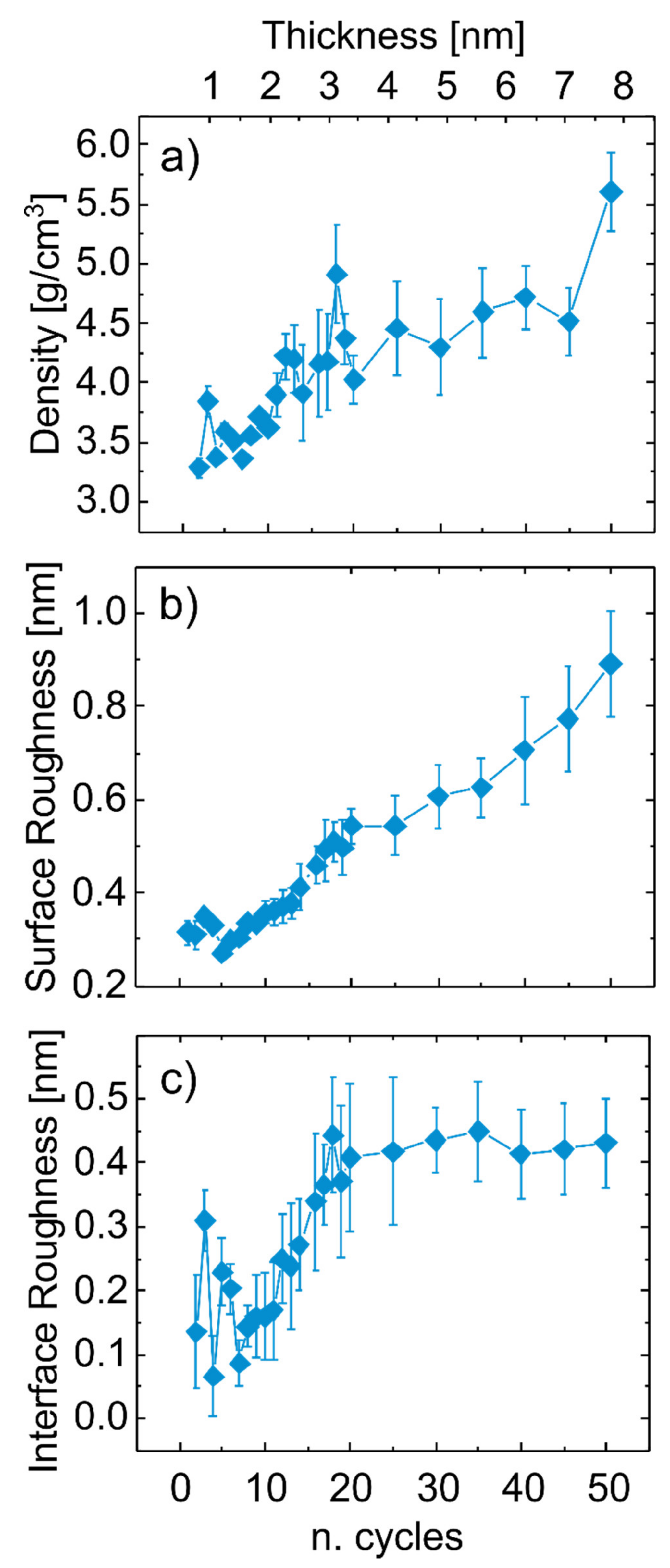
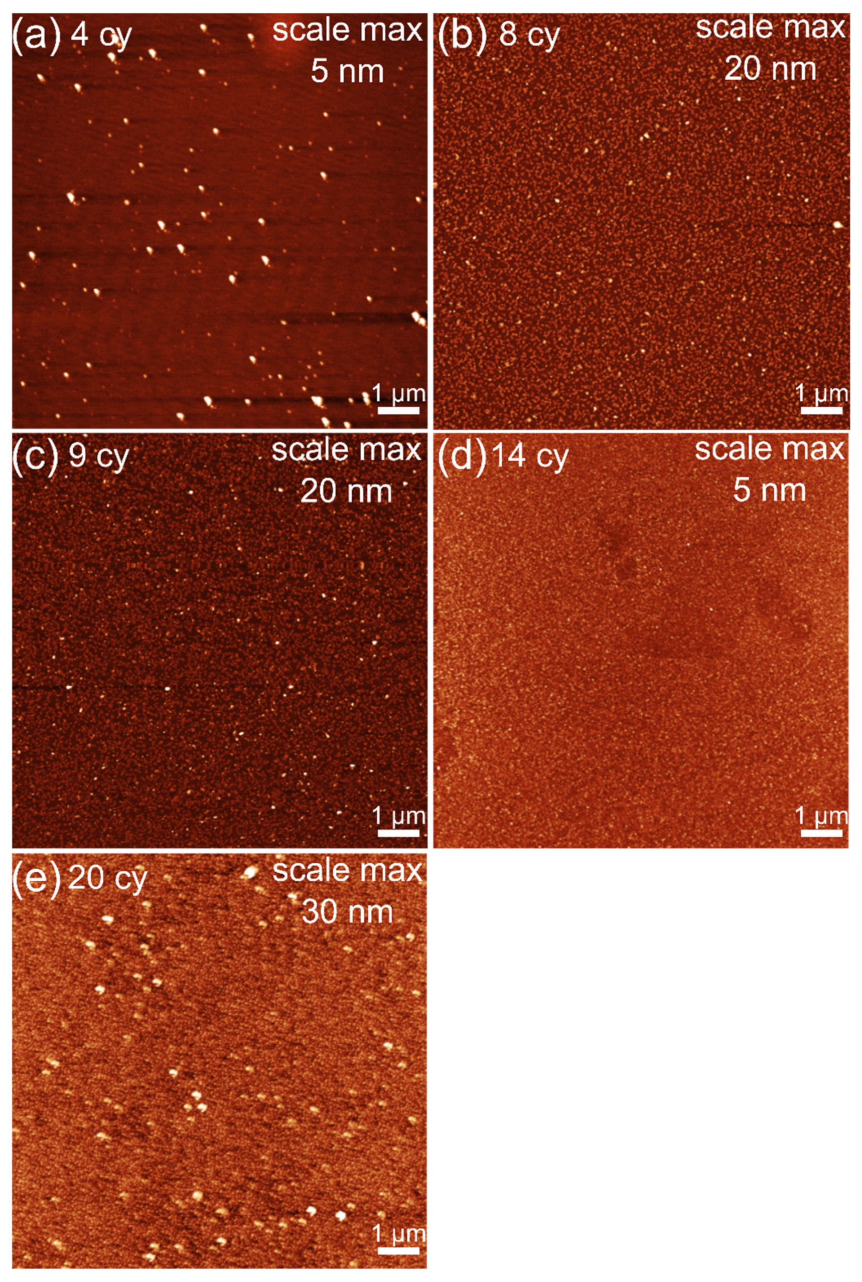
3.1. Thickness and Morphology

ZnO thin films were prepared at room temperature by PE-ALD, as previously reported [18], and the thickness was varied by varying the number of cycles from 1 to 50 resulting in a maximum thickness of about 8 nm. X-ray reflectivity (XRR) measurements of the respective samples were carried out to follow the evolution of the thickness of the growing ZnO (Figure 1).
The XRR curves in Figure 1a show a high intensity for low angles, which is the region of total reflection. At the critical angle (around 2θ = 0.44–0.47°), the intensity rapidly drops showing the capability of the X-ray beam to penetrate into the layer. Typically, the angle is related to the electron density of the top layer, but as ZnO is thin and the native SiO2 layer has a comparable thickness value, useful information on the density cannot be directly extracted. After the critical angle, the intensity decays further for higher angles according to Fresnel’s law. By increasing the thickness of the top ZnO starting from one cycle, Kiessig fringes appear in the curves due to thickness-dependent interference effects visible in a clear minimum between 3 and 4.5°. The period of these fringes decreases with increasing number of cycles; thus, it is inversely correlated to the thickness. Using a model-dependent fitting, film properties such as the thickness, density, and surface and interface roughness can be derived from the XRR curves. The modelled thickness as a function of the number of cycles is shown in Figure 1b. For the first few cycles (up to 10 cycles), the thickness increases rapidly. After this transient growth region, the rate slightly decreases and shows a linear behavior throughout the investigated range (50 cycles). Differentiating the thickness vs. number of cycles curve, the growth per cycle (GPC) can be obtained (Figure 1c). The GPC is about 0.85 nm for the first cycle, and afterwards decreases with the numbers of cycles. After 10 cycles the GPC was found constant with a value of around 0.16 nm and does not appear to change up to 50 cycles.
Puurunen et al. [33] proposed four different models to describe the variation of the GPC in the initial stages of the growth. These are 1) linear growth (constant GPC for all number of cycles), 2) substrate-enhanced growth (higher GPC in the beginning followed by a decrease to a constant value), 3) substrate-inhibited growth type 1 (lower GPC in the beginning followed by an increase to a constant value, and 4) substrate-inhibited growth type 2 (first increase to a maximum and then decrease to constant value). Following this classification, the GPC trend shown in Figure 1c can be identified as substrate-enhanced growth. The first cycle shows the highest difference to the steady-state value and the GPC for 2 to 8 cycles rapidly drops to 0.16 nm. In the literature, for the initial growth of thermal ALD of ZnO, the GPC behavior is often reported with a “substrate-inhibited”-like behavior on different substrates such as a-SiO2 [23], In0.53Ga0.47As [29], and Al2O3 [25]. In these studies, the first cycles of the ZnO growth were characterized by island formation, with a limited thickness development, as measured by in-situ XRR and XRF. In our contribution, the effect of the oxygen plasma in direct contact with the substrate is believed to increase the number of reactive sites available for the DEZ molecules, enhancing the growth, similarly to the increase in hydrophilic properties of the Si wafers adopted in the semiconductor industry prior to wafer bonding [45]. A similar behavior was reported for the growth of AlN when comparing thermal and plasma enhanced-ALD [46].
With the purpose of better understanding the ZnO growth, additional material properties are shown in Figure 2, i.e., mass density, surface and interface roughness, derived from the fitting of the XRR data.
For the transient regime, the mass density fluctuates around a value of 3.5 ± 0.2 g cm−3, the roughness around a value of 0.32 ± 0.02 nm and the interface roughness around 0.19 ± 0.06 nm. For more than 10 cycles, the mass density increases rapidly for a few cycles and slows down afterwards, with the values being between 4.2 ± 0.3 and 4.5 ± 0. 3 g cm−3. These values increase for thicker films, up to a mass density of 5.6 g cm−3, as measured on a 30-nm-thick ZnO [39]. The surface roughness shows a fairly linear increase after 10 cycles and the interface roughness also increases at first until it reaches a constant value of around 0.4 nm at 20 cycles. The interface roughness values point out the completion of the interface between the ZnO layer and the a-SiO2 above 10 cycles, suggesting the formation of a continuous layer in correspondence with a constant GPC, as shown in Figure 2c.
A model-independent method was also used to fit the data in Figure 1 to verify the robustness of the prior adopted three-layer model and exclude a mutual dependence of the model variables. The normalized electron density profiles of several films obtained are shown in Figure 3. Below six cycles, the fitting procedure did not converge to feasible results, indicating a highly structured surface and corroborating the hypothesis of a non-continuous layer in the first cycles of growth. After six cycles feasible results converged from the model independent fitting and some of the data are summarized in Figure 3. For −1 < z < 0 nm, the electron density values represent the c-Si substrate and are normalized to 1. The onset of the electron density increases at z = 0 nm, reflecting the electron density of the native oxide layer, which is about 1 nm for all samples. The electron density then rapidly increases and finally reaches plateau values which can be generalized in two groups; up until 10 cycles, the normalized electron density of the films is around 1.7, whereas for films above 10 cycles the normalized electron density saturates at around 2.0. The values of the reported electron density correspond to mass density values (assuming a stoichiometric ZnO film) of 3.1 and 3.7 g cm−3, respectively. The trend of the density (i.e., two plateaus for the transient and steady-state region) agrees well with the fitting using the model-dependent software. However, an offset of around 0.5 g cm−3 is apparent, which could be due to stoichiometric assumptions. In fact, thicker ZnO layers deposited at room temperature showed a lower mass density as bulk ZnO, as mentioned above. The roughness is represented by the slope of the electron density toward the surface to air, which is located at the right hand side of the curves or larger z values. The slope does not show large variations until 17 cycles, where it mildens, corresponding to an increase in surface roughness.
Both model-dependent (Figure 2) and model-independent (Figure 3) results identify the two distinct regions of growth. In order to further confirm the so-far observed trend, additional experimental techniques were employed. The thickness measured by SE and the Zn amount measured by XRF as a function of the number of cycles is shown in Figure 4.
The thickness by SE shows the same trend as the one obtained with XRR measurement, i.e., an initial region with a slightly enhanced growth followed by a transition to a steady-state growth. The roughness could not be implemented in the SE model without giving unphysical or non-significant values. For the amount of Zn measured by XRF, no significant deviation from a constant slope can be observed as function of the number of cycles. The slight difference in rate between the obtained thickness (by XRR and SE) and the zinc amount (by XRF) in the transient region might occur due to morphological considerations. This means that while the same zinc amount is deposited per cycle, as expected being in a self-limiting regime [18], the measured thickness might not be the same due to changes in the structure and mass density.
In order to complete the morphological picture of the ZnO layers and shed light on the initial growth modes, AFM height images of films prepared with different number of cycles at room temperature are shown in Figure 5.
The AFM images reveal scattered island deposited in the first cycles of deposition, similar to the work of Baji et al. for ZnO deposited at 150 °C by thermal ALD [24]. For four cycles (Figure 5a), scattered islands are found on the surface and the coverage is below 2%. Line scans reveal larger islands with diameters of around 100 nm and heights of around 6 nm and smaller islands with a diameter of around 50 to 60 nm and height of around 1 nm. Increasing the number of cycles to 8 and 9 cycles (Figure 5b,c) leads to an increase in coverage to around 25% and the island height increases to a maximum of 3 to 4 nm, whereas the diameter stays around 50 nm. A coalescence of the islands resulting in a closed and smooth layer is observed at 14 cycles (Figure 5d), whereas the size of the coalescing islands is still around 50 nm. The stage at which a continuous layer is achieved (according to the AFM images around 14 cycles) is also in agreement with other investigated material properties. A large change in the mass density was shown for films grown after a similar number of cycles (see Figure 2 and Figure 3). Furthermore, the GPC settles to a constant value at this stage (Figure 1), which indicates the initialization of the ALD-typical layer-by-layer growth. By further increasing the number of cycles to 20 cycles (Figure 5e), the roughness increases compared to the 14 cycles sample and there are areas with increased height. This increased height suggests the development of crystallites. Baji et al. [24] investigated the initial stages of growth of ZnO by thermal ALD on different substrates. The growth on Si (with native oxide) showed a similar trend for the morphology to our results, that is, scattered islands at 5 and 10 cycles, and a full coverage above 15 cycles. In a nutshell, the AFM results suggest an island growth for the initial stages whereas the number of islands with diameters of around 50 nm increases with increasing number of cycles (4 to 9 cycles). After forming a closed layer by coalescence (around 14 cycles), an increase in height and roughness is observed (20 cycles), suggesting the formation of crystallites.
In summary, the combination of XRR, XRF, SE, and AFM revealed an enhanced island-growth mode for direct plasma ALD on Si substrates. Scattered islands are formed in the first cycles, with a higher mass density compared to thermal ALD of ZnO, resulting in a higher apparent thickness of the growing layer. The plasma is believed to increase the number of available nucleation sites, which grow in number and height after every cycle. A higher mobility of the species on the surface is to be excluded, considering that the deposition is run at room temperature. On the contrary, the islands are forming and quickly growing in the first ALD cycles, supporting the hypothesis of an active role of the direct plasma in the formation of additional reactive sites. In the literature, Napari et al. [47] reported on a comparison between the growth of ZnO obtained by remote and direct plasma sources in PE-ALD at room temperature. They also reported a generally higher GPC for the direct plasma growth compared to the remote one, due to the higher flux density of plasma species actively contributing to the material growth. A continuous layer is formed between cycle 10 and 14, with a thickness of 2 nm. Mass density, surface and interface roughness are increasing steeply starting from this stage, while the GPC starts to have a constant value.

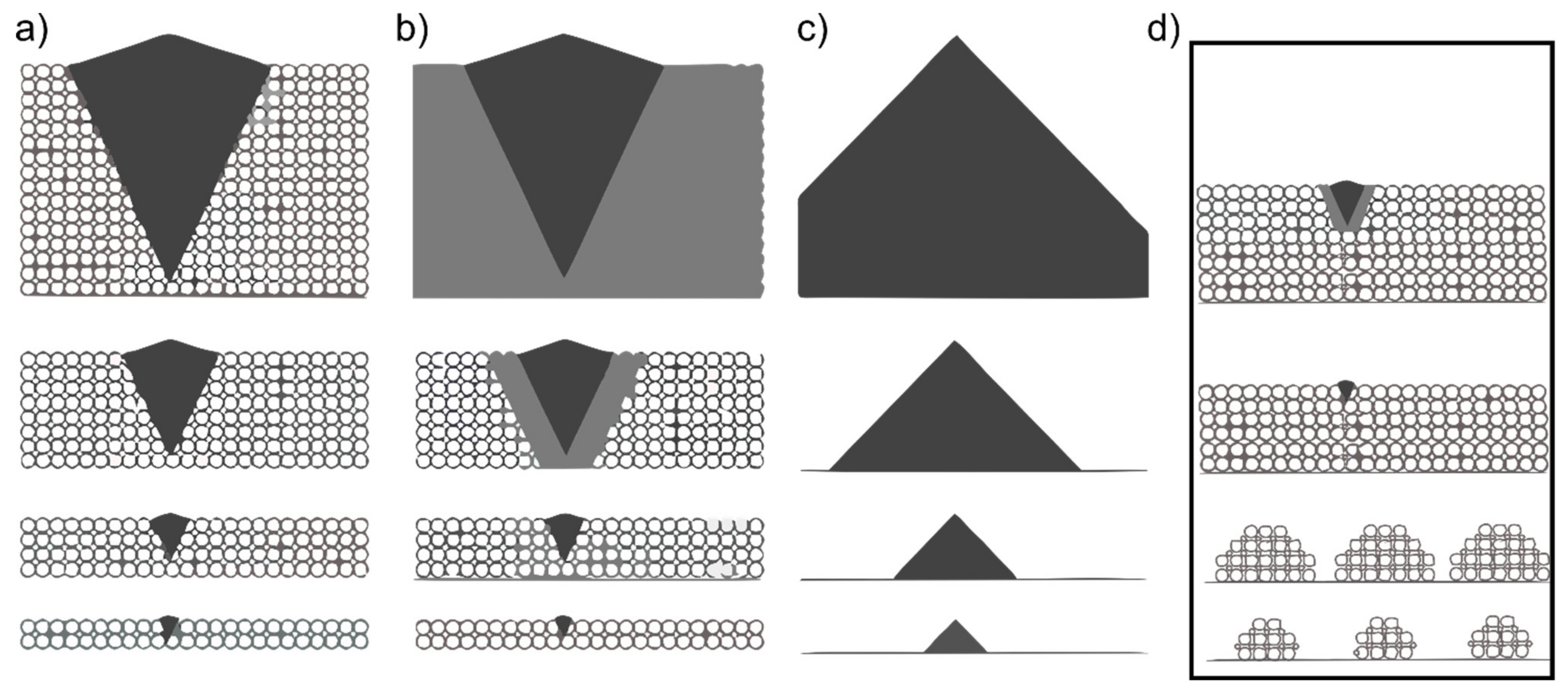
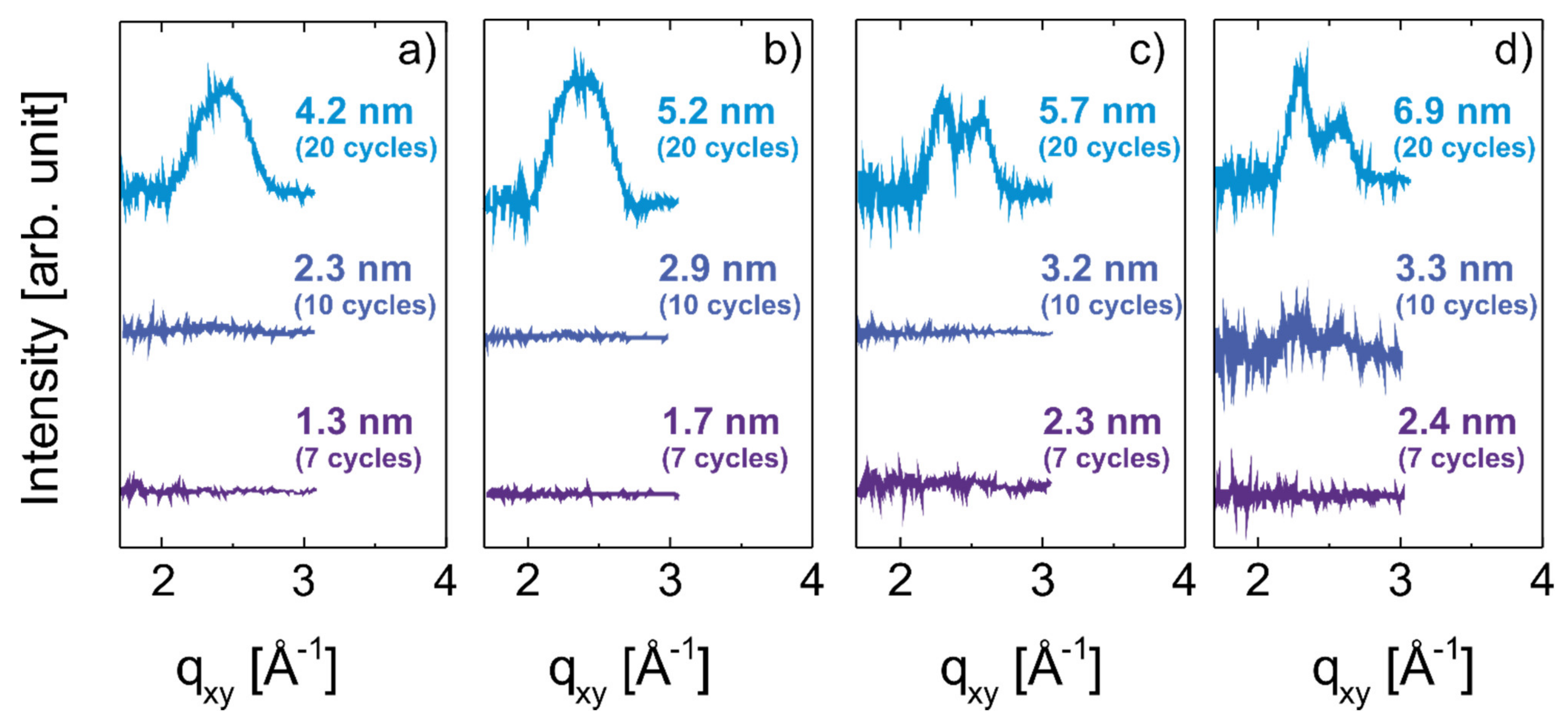
3.2. Development of Crystallites

The onset of the crystalline ZnO was also investigated, as polycrystalline ZnO layers with a 100 texture had been obtained for thicker layers grown at room temperature with PE-ALD [18]. To investigate the beginning of the crystallization, GIXD was performed on the films with different thickness. Such a measurement allows the gathering of structural information down to monolayers extension from the substrate. An example for a reciprocal space map of a ZnO film is shown in Figure 6a.
For polycrystalline samples, the so called Scherrer rings will appear in the space map, indicating the in-plane and near out-of-plane (excluding specular) orientation of the crystallites. To see at which cycle number crystalline features appear in the film, a linear integration was performed around the in-plane direction (qz = 0 Å−1) (indicated in Figure 6a). The intensity as a function of qxy for samples of different thickness prepared at room temperature is shown in Figure 6b. For thicknesses up to 10 cycles, peaks cannot be observed. This either indicates an amorphous layer in the first stages of growth or the lateral (in-plane) size of the crystallites is too small so that not enough diffracted intensity can be generated to be detected. Starting from 20 cycles, a rather broad peak appears at around 2.5 Å−1. The deconvolution of such a peak allows for the distinction of a contribution at 2.41 Å−1, and 2.54 Å−1, attributed to the (002) and (101) orientation, respectively, when compared to the reference ZnO powder (26170-ICSD). [48] No signal from the (100) orientation at 2.23 Å−1 is present. This is in agreement with the (100) preferential orientation in the specular direction previously reported at room temperature [18,38,39]. When integrating the signal for the in-plane orientation, a peak arises originating from the (002) planes perpendicular to the substrate surface. In the literature, the ZnO crystallization is generally reported as island crystallites growing and coalescing before giving a layer-by-layer growth [22]. In a series of works on the initial growth of thermal ALD of ZnO, Ciatto et al. [26,27,28] focused on the crystal formation in the early stages of the ZnO growth. By means of in-situ X-ray based techniques, a 2D structure was identified in the first cycles of growth, with an in-plane crystallinity developing as early as from the second cycle when deposited on a-Si. A (001) fiber texture developed, together with grains, showing no preferential texture. However, in this study, no grain growth was witnessed in the first 10 cycles, that is, until a continuous layer is formed. Instead, in our work the onset of the crystallization starts after the completion of a continuous layer. The first 2.5 to 3 nm of growth (corresponding to the first 20 cycles) are amorphous, indicating that the enhanced island growth has no long-range ordering. The onset of crystallization corresponds to the beginning of the layer-by-layer growth. Furthermore, mass density, surface and interface roughness have an abrupt change in trend after the onset, as mentioned above. The crystallites grow with the number of cycles, and for a thickness of 45 nm we earlier reported crystallite sizes close to 30 nm [18]. Thus, the crystallization is thought to start once a closed amorphous layer is formed. In the extensive review on the crystallization of inorganic materials by ALD, Puurunen et al. [22] identified three possible modes for the crystallization onset, schematically reported in Figure 7a–c.
The initial growth of ZnO via direct-plasma enhanced ALD presented here shows an intermediate behavior between the crystalline island growth (Figure 7c) and the formation of an amorphous region, followed by formation in the amorphous material of the crystallite (Figure 7b). The formation of additional reactive sites on the substrate surface due to the direct plasma develops an initial amorphous growth of the ZnO clusters, followed first by a coalescence of the amorphous islands and formation of the initial crystal nuclei. Generally, for ALD the plasma was found to accelerate the onset of the crystallization [22]. However, earlier studies focusing on the (self-)texture development of ZnO adopting (plasma-based) sputtering or chemical vapor deposition methods highlighted the possibility of the formation of an amorphous region prior to the crystallization onset [49,50]. Moreover, an amorphous initial layer was also reported for thermal ALD of ZnO deposited on a-SiO2 [23] and recently on In0.53Ga0.47As [29]. In a recent in-situ study on the effect of annealing on PE-ALD ZnO, we demonstrated the presence of an amorphous fraction of material in the room-temperature-deposited ZnO [38], supporting the hypothesis of its initial amorphous growth.

3.3. Crystallization at High Temperature

The ALD initial growth and crystallization studies reported so far investigated processes run at high temperature, i.e., starting from 100 °C. With the aim of verifying if the room temperature processes adopted in this study have an influence on the onset of crystallization, considering the lower surface mobility, higher sticking coefficient and lower energy of the species at this temperature, the same GIXD analysis was performed for samples with increasing thickness prepared at different substrate temperatures. The intensity plots for substrate temperatures from 50 to 200 °C are shown in Figure 8a–d.
Similar to the room temperature sample, a peak appears above 3 nm, irrespective of the substrate temperature. (Figure 8a–c). Starting from 150 °C, peaks corresponding to the (100) and (101) in-plane orientation are distinguishable and show similar intensity. For the sample prepared at 200 °C (Figure 8d), peaks can be observed already at 3.3 nm. Compared to the 150 °C sample, the (100) in-plane orientation shows an enhanced intensity. This temperature dependence of the preferential orientation is known and has already been shown in the literature for thicker films [51,52]. Considering that the growth per cycle increases with increasing temperature (i.e., the same number of cycles at higher temperature results in a thicker film than for a lower temperature), the development of crystallinity seems to happen at a thickness above 3 nm, irrespective of the crystalline orientation and deposition temperature. This result excludes the contribution of these parameters in the formation of an initial amorphous layer and corroborates the hypothesis of the role of the direct plasma in enhancing the initial growth at the expenses of the long-range order.

4. Conclusions

The initial growth of polycrystalline ZnO deposited at room temperature by direct PE-ALD on Si with native oxide is investigated. Different ex-situ characterization methods (XRR, SE, XRF, and AFM) allowed the identification of an additional growth mechanism for inorganic materials deposited by ALD. An accelerated island growth was found to occur in the first stages of layer formation, with a behavior in between the classical substrate-accelerated and island growth previously identified for inorganic ALD layers. In the initial 14 to 20 cycles, corresponding to 2.5 to 3 nm of material, an elevated number of islands of ZnO are forming. Increasing the number of cycles, the islands were found to coalesce and a classical layer-by-layer mechanism was identified. Furthermore, by adopting synchrotron radiation GIXD, the onset of crystallization was studied. Differently from the classical ALD island growth model, amorphous islands are grown in the first stages. The first crystallites are formed after the islands coalesce, that is, starting from roughly 3 nm. The direct plasma adopted as co-reactant is believed to accelerate the island formation and prevent an initial crystallization by increasing the number of reactive sites present on the substrate surface. The onset of crystallization was additionally studied at high temperature to better identify the origin of the late crystallite formation. Irrespective of temperature and crystal orientation, an amorphous layer with a minimum thickness of 3.2 nm was witnessed.
This investigation extends the knowledge on the initial growth of inorganic materials adopting ALD and highlights the need for further efforts in studying the role of plasma in deviating from the classical growth-models.

Author Contributions

Conceptualization, methodology, implementation and writing: A.P. and J.P.; AFM methodology and data curation, O.W.; XRR data curation: R.R.; writing—review and editing, A.P., J.P., A.M.C., O.W., R.R.; supervision, A.M.C., R.R.; funding acquisition, A.M.C. All authors have read and agreed to the published version of the manuscript.

Funding

This research was funded by European Research Council (ERC) under the European Union’s Horizon 2020 research and innovation program (grant agreement 715403).

Acknowledgments

The authors thank Elettra Sincrotrone Trieste for the allocation of synchrotron radiation beamtime and L. Barba and M. Polentarutti for aiding with the beamline XRD1. Open Access Funding by the Graz University of Technology is also gratefully acknowledged.

Conflicts of Interest

The authors declare no conflict of interest. The funders had no role in the design of the study; in the collection, analyses, or interpretation of data; in the writing of the manuscript, or in the decision to publish the results.

References

  1. Yu, X.; Marks, T.J.; Facchetti, A. Metal oxides for optoelectronic applications. Nat. Mater. 2016, 15, 383–396. [Google Scholar] [CrossRef] [PubMed]
  2. Klingshirn, C.; Fallert, J.; Zhou, H.; Sartor, J.; Thiele, C.; Maier-Flaig, F.; Schneider, D.; Kalt, H. 65 years of ZnO research–old and very recent results. Phys. Status Solidi 2010, 247, 1424–1447. [Google Scholar] [CrossRef]
  3. Arya, S.K.; Saha, S.; Ramirez-Vick, J.E.; Gupta, V.; Bhansali, S.; Singh, S.P. Recent advances in ZnO nanostructures and thin films for biosensor applications: Review. Anal. Chim. Acta 2012, 737, 1–21. [Google Scholar] [CrossRef] [PubMed]
  4. Tynell, T.; Karppinen, M. Atomic layer deposition of ZnO: A review. Semicond. Sci. Technol. 2014, 29, 043001. [Google Scholar] [CrossRef]
  5. Cachoncinlle, C.; Hebert, C.; Perrière, J.; Nistor, M.; Petit, A.; Millon, E. Random lasing of ZnO thin films grown by pulsed-laser deposition. Appl. Surf. Sci. 2015, 336, 103–107. [Google Scholar] [CrossRef]
  6. Özgür, Ü.; Alivov, Y.I.; Liu, C.; Teke, A.; Reshchikov, M.A.; Doğan, S.; Avrutin, V.; Cho, S.-J.; Morkoç, H. A comprehensive review of ZnO materials and devices. J. Appl. Phys. 2005, 98, 041301. [Google Scholar] [CrossRef] [Green Version]
  7. Wu, Y.; Hermkens, P.M.; Van de Loo, B.W.H.; Knoops, H.C.M.; Potts, S.E.; Verheijen, M.A.; Roozeboom, F.; Kessels, W.M.M. Electrical transport and Al doping efficiency in nanoscale ZnO films prepared by atomic layer deposition. J. Appl. Phys. 2013, 114, 024308. [Google Scholar] [CrossRef]
  8. Lee, D.-J.; Kim, H.-M.; Kwon, J.-Y.; Choi, H.; Kim, S.-H.; Kim, K.-B. Structural and Electrical Properties of Atomic Layer Deposited Al-Doped ZnO Films. Adv. Funct. Mater. 2011, 21, 448–455. [Google Scholar] [CrossRef]
  9. Horwat, D.; Mickan, M.; Chamorro, W. New strategies for the synthesis of ZnO and Al-doped ZnO films by reactive magnetron sputtering at room temperature. Phys. Status Solidi 2016, 13, 951–957. [Google Scholar] [CrossRef]
  10. Wisz, G.; Virt, I.; Sagan, P.; Potera, P.; Yavorskyi, R. Structural, Optical and Electrical Properties of Zinc Oxide Layers Produced by Pulsed Laser Deposition Method. Nanoscale Res. Lett. 2017, 12, 253. [Google Scholar] [CrossRef] [Green Version]
  11. Kim, D.; Kang, H.; Kim, J.M.; Kim, H. The properties of plasma-enhanced atomic layer deposition (ALD) ZnO thin films and comparison with thermal ALD. Appl. Surf. Sci. 2011, 257, 3776–3779. [Google Scholar] [CrossRef]
  12. Baitimirova, M.; Viter, R.; Andzane, J.; Van der Lee, A.; Voiry, D.; Iatsunskyi, I.; Coy, E.; Mikoliunaite, L.; Tumenas, S.; Załęski, K.; et al. Tuning of Structural and Optical Properties of Graphene/ZnO Nanolaminates. J. Phys. Chem. C 2016, 120, 23716–23725. [Google Scholar] [CrossRef]
  13. Graniel, O.; Weber, M.; Balme, S.; Miele, P.; Bechelany, M. Atomic layer deposition for biosensing applications. Biosens. Bioelectron. 2018, 122, 147–159. [Google Scholar] [CrossRef] [PubMed]
  14. Abou Chaaya, A.; Viter, R.; Bechelany, M.; Alute, Z.; Erts, D.; Zalesskaya, A.; Kovalevskis, K.; Rouessac, V.; Smyntyna, V.; Miele, P. Evolution of microstructure and related optical properties of ZnO grown by atomic layer deposition. Beilstein J. Nanotechnol. 2013, 4, 690–698. [Google Scholar] [CrossRef] [PubMed] [Green Version]
  15. Oruc, F.B.; Aygun, L.E.; Donmez, I.; Biyikli, N.; Okyay, A.K.; Yu, H.Y. Low temperature atomic layer deposited ZnO photo thin film transistors. J. Vac. Sci. Technol. A Vacuum Surf. Film 2015, 33, 01A105. [Google Scholar] [CrossRef]
  16. Tereshchenko, A.; Bechelany, M.; Viter, R.; Khranovskyy, V.; Smyntyna, V.; Starodub, N.; Yakimova, R. Optical biosensors based on ZnO nanostructures: Advantages and perspectives. A review. Sens. Actuators B Chem. 2016, 229, 664–677. [Google Scholar] [CrossRef]
  17. Rowlette, P.C.; Allen, C.G.; Bromley, O.B.; Dubetz, A.E.; Wolden, C.A. Plasma-enhanced atomic layer deposition of semiconductor grade ZnO using dimethyl zinc. Chem. Vap. Depos. 2009, 15, 15–20. [Google Scholar] [CrossRef]
  18. Pilz, J.; Perrotta, A.; Christian, P.; Tazreiter, M.; Resel, R.; Leising, G.; Griesser, T.; Coclite, A.M. Tuning of material properties of ZnO thin films grown by plasma-enhanced atomic layer deposition at room temperature. J. Vac. Sci. Technol. A Vacuum Surf. Film 2018, 36, 01A109. [Google Scholar] [CrossRef] [Green Version]
  19. Thomas, M.A.; Cui, J.B. Highly tunable electrical properties in undoped ZnO grown by plasma enhanced thermal-atomic layer deposition. ACS Appl. Mater. Interfaces 2012, 4, 3122–3128. [Google Scholar] [CrossRef]
  20. Thomas, M.A.; Cui, J. The Effects of an O2 Plasma on the Optical Properties of Atomic Layer Deposited ZnO. ECS Trans. 2012, 45, 87–95. [Google Scholar] [CrossRef]
  21. Profijt, H.B.; Potts, S.E.; Van de Sanden, M.C.M.; Kessels, W.M.M. Plasma-Assisted Atomic Layer Deposition: Basics, Opportunities, and Challenges. J. Vac. Sci. Technol. A Vacuum Surf. Film 2011, 29, 050801. [Google Scholar] [CrossRef] [Green Version]
  22. Miikkulainen, V.; Leskelä, M.; Ritala, M.; Puurunen, R.L. Crystallinity of inorganic films grown by atomic layer deposition: Overview and general trends. J. Appl. Phys. 2013, 113, 021301. [Google Scholar] [CrossRef]
  23. Fong, D.D.; Eastman, J.A.; Kim, S.K.; Fister, T.T.; Highland, M.J.; Baldo, P.M.; Fuoss, P.H. In situ synchrotron x-ray characterization of ZnO atomic layer deposition. Appl. Phys. Lett. 2010, 97, 191904. [Google Scholar] [CrossRef]
  24. Baji, Z.; Lábadi, Z.; Horváth, Z.E.; Molnár, G.; Volk, J.; Bársony, I.; Barna, P. Nucleation and Growth Modes of ALD ZnO. Cryst. Growth Des. 2012, 12, 5615–5620. [Google Scholar] [CrossRef]
  25. Klug, J.A.; Weimer, M.S.; Emery, J.D.; Yanguas-Gil, A.; Seifert, S.; Schlepütz, C.M.; Martinson, A.B.F.; Elam, J.W.; Hock, A.S.; Proslier, T. A modular reactor design for in situ synchrotron x-ray investigation of atomic layer deposition processes. Rev. Sci. Instrum. 2015, 86, 113901. [Google Scholar] [CrossRef] [PubMed] [Green Version]
  26. Boichot, R.; Tian, L.; Richard, M.-I.; Crisci, A.; Chaker, A.; Cantelli, V.; Coindeau, S.; Lay, S.; Ouled, T.; Guichet, C.; et al. Evolution of Crystal Structure During the Initial Stages of ZnO Atomic Layer Deposition. Chem. Mater. 2016, 28, 592–600. [Google Scholar] [CrossRef]
  27. Chu, M.H.; Tian, L.; Chaker, A.; Cantelli, V.; Ouled, T.; Boichot, R.; Crisci, A.; Lay, S.; Richard, M.-I.; Thomas, O.; et al. An Atomistic View of the Incipient Growth of Zinc Oxide Nanolayers. Cryst. Growth Des. 2016, 16, 5339–5348. [Google Scholar] [CrossRef]
  28. Chu, M.-H.; Tian, L.; Chaker, A.; Skopin, E.; Cantelli, V.; Ouled, T.; Boichot, R.L.; Crisci, A.; Lay, S.; Richard, M.-I.; et al. Evaluation of Alternative Atomistic Models for the Incipient Growth of ZnO by Atomic Layer Deposition. J. Electron. Mater. 2017, 46, 3512–3517. [Google Scholar] [CrossRef]
  29. Skopin, E.V.; Rapenne, L.; Roussel, H.; Deschanvres, J.-L.; Blanquet, E.; Ciatto, G.; Fong, D.D.; Richard, M.-I.; Renevier, H. The initial stages of ZnO atomic layer deposition on atomically flat In0.53Ga0.47As substrates. Nanoscale 2018, 10, 11585–11596. [Google Scholar] [CrossRef]
  30. Skopin, E.V.; Deschanvres, J.-L.; Renevier, H. In Situ Ellipsometry Study of the Early Stage of ZnO Atomic Layer Deposition on In0.53Ga0.47As. Phys. Status Solidi 2020, 86, 1900831. [Google Scholar] [CrossRef]
  31. Liao, M.-H.; Chang, L.C. Experimental demonstration for the implant-free In0.53Ga0.47As quantum-well metal-insulator-semiconductor field-effect transistors with ultra-low source/drain resistance. Appl. Phys. Lett. 2013, 103, 072102. [Google Scholar] [CrossRef]
  32. Hyun Kim, S.; Yeong Joo, S.; Soo Jin, H.; Kim, W.-B.; Joo Park, T. Ultrathin ZnS and ZnO Interfacial Passivation Layers for Atomic-Layer-Deposited HfO2 Films on InP Substrates. ACS Appl. Mater. Interfaces 2016, 8, 20880–20884. [Google Scholar]
  33. Puurunen, R.L.; Vandervorst, W. Island growth as a growth mode in atomic layer deposition: A phenomenological model. J. Appl. Phys. 2004, 96, 7686–7695. [Google Scholar] [CrossRef]
  34. Langereis, E.; Heil, S.B.S.; Van de Sanden, M.C.M.; Kessels, W.M.M. In situ spectroscopic ellipsometry study on the growth of ultrathin TiN films by plasma-assisted atomic layer deposition. J. Appl. Phys. 2006, 100, 023534. [Google Scholar] [CrossRef] [Green Version]
  35. Langereis, E.; Heil, S.B.S.; Knoops, H.C.M.; Keuning, W.; Van de Sanden, M.C.M.; Kessels, W.M.M. In situ spectroscopic ellipsometry as a versatile tool for studying atomic layer deposition. J. Phys. D Appl. Phys. 2009, 42, 073001. [Google Scholar] [CrossRef] [Green Version]
  36. Dendooven, J.; Solano, E.; Minjauw, M.M.; Van de Kerckhove, K.; Coati, A.; Fonda, E.; Portale, G.; Garreau, Y.; Detavernier, C. Mobile setup for synchrotron based in situ characterization during thermal and plasma-enhanced atomic layer deposition. Rev. Sci. Instrum. 2016, 87, 113905. [Google Scholar] [CrossRef] [Green Version]
  37. Perrotta, A.; Pilz, J.; Pachmajer, S.; Milella, A.; Coclite, A.M. On the transformation of “zincone”-like into porous ZnO thin films from sub-saturated plasma enhanced atomic layer deposition. Beilstein J. Nanotechnol. 2019, 10, 746–759. [Google Scholar] [CrossRef]
  38. Perrotta, A.; Pilz, J.; Milella, A.; Coclite, A.M. Opto-chemical control through thermal treatment of plasma enhanced atomic layer deposited ZnO: An in situ study. Appl. Surf. Sci. 2019, 483, 10–18. [Google Scholar] [CrossRef]
  39. Pilz, J.; Perrotta, A.; Leising, G.; Coclite, A.M. ZnO Thin Films Grown by Plasma-Enhanced Atomic Layer Deposition: Material Properties within and Outside the “ALD Window.”. Phys. Status Solidi 2019, 1900256. [Google Scholar] [CrossRef] [Green Version]
  40. Knoops, H.C.M.; Van de Loo, B.W.H.; Smit, S.; Ponomarev, M.V.; Weber, J.-W.; Sharma, K.; Kessels, W.M.M.; Creatore, M. Optical modeling of plasma-deposited ZnO films: Electron scattering at different length scales. J. Vac. Sci. Technol. A Vacuum Surf. Film 2015, 33, 021509. [Google Scholar] [CrossRef] [Green Version]
  41. Danauskas, S.M.; Li, D.; Meron, M.; Lin, B.; Lee, K.Y.C. Stochastic fitting of specular X-ray reflectivity data using StochFit. J. Appl. Crystallogr. 2008, 41, 1187–1193. [Google Scholar] [CrossRef]
  42. Lausi, A.; Polentarutti, M.; Onesti, S.; Plaisier, J.R.; Busetto, E.; Bais, G.; Barba, L.; Cassetta, A.; Campi, G.; Lamba, D.; et al. Status of the crystallography beamlines at Elettra. Eur. Phys. J. Plus 2015, 130, 43. [Google Scholar] [CrossRef]
  43. Schrode, B.; Pachmajer, S.; Dohr, M.; Röthel, C.; Domke, J.; Fritz, T.; Resel, R.; Werzer, O. IUCr GIDVis: A comprehensive software tool for geometry-independent grazing-incidence X-ray diffraction data analysis and pole-figure calculations. J. Appl. Crystallogr. 2019, 52, 683–689. [Google Scholar] [CrossRef] [Green Version]
  44. Nečas, D.; Klapetek, P. Gwyddion: An open-source software for SPM data analysis. Cent. Eur. J. Phys. 2012, 10, 181–188. [Google Scholar] [CrossRef]
  45. Kim, S.W.; Peng, L.; Miller, A.; Beyer, G.; Beyne, E.; Lee, C.S. Permanent wafer bonding in the low temperature by using various plasma enhanced chemical vapour deposition dielectrics. In Proceedings of the 2015 International 3D Systems Integration Conference, 3DIC 2015, Sendai, Japan, 31 August–2 September 2015; Institute of Electrical and Electronics Engineers Inc.: Tokyo, Japan, 2015; pp. TS7.2.1–TS7.2.4. [Google Scholar]
  46. Van Bui, H.; Wiggers, F.B.; Gupta, A.; Nguyen, M.D.; Aarnink, A.A.I.; De Jong, M.P.; Kovalgin, A.Y. Initial growth, refractive index, and crystallinity of thermal and plasma-enhanced atomic layer deposition AlN films. J. Vac. Sci. Technol. A Vacuum Surf. Film 2015, 33, 01A111. [Google Scholar] [CrossRef]
  47. Napari, M.; Lahtinen, M.; Veselov, A.; Julin, J.; Østreng, E.; Sajavaara, T. Room-temperature plasma-enhanced atomic layer deposition of ZnO: Film growth dependence on the PEALD reactor configuration. Surf. Coat. Technol. 2017, 326, 281–290. [Google Scholar] [CrossRef] [Green Version]
  48. Abrahams, S.C.; Bernstein, J.L. Remeasurement of the structure of hexagonal ZnO. Acta Crystallogr. Sect. B Struct. Crystallogr. Cryst. Chem. 1969, 25, 1233–1236. [Google Scholar] [CrossRef]
  49. Koch, M.H.; Hartmann, A.J.; Lamb, R.N.; Neuber, M.; Grunze, M. Self-Texture in the Initial Stages of ZnO Film Growth. J. Phys. Chem. B 1997, 101, 8231–8236. [Google Scholar] [CrossRef]
  50. Kajikawa, Y. Texture development of non-epitaxial polycrystalline ZnO films. J. Cryst. Growth 2006, 289, 387–394. [Google Scholar] [CrossRef]
  51. Park, S.-H.K.; Hwang, C.-S.; Kwack, H.-S.; Lee, J.-H.; Chu, H.Y. Characteristics of ZnO Thin Films by Means of Plasma-Enhanced Atomic Layer Deposition. Electrochem. Solid-State Lett. 2006, 9, G299–G301. [Google Scholar] [CrossRef]
  52. Zhang, J.; Yang, H.; Zhang, Q.; Dong, S.; Luo, J.K. Structural, optical, electrical and resistive switching properties of ZnO thin films deposited by thermal and plasma-enhanced atomic layer deposition. Appl. Surf. Sci. 2013, 282, 390–395. [Google Scholar] [CrossRef]
Figure 1. (a) XRR curves of the first (top) up to the 20th (bottom) PE-ALD ZnO cycle; the curves are stacked for clarity. The fitting curves are also reported with a red dashed line; (b) modelled ZnO layer thickness as determined from the XRR curves adopting a three-layer model vs. number of cycles; (c) growth per cycle (GPC) calculated from the XRR-derived thickness for all samples.
Crystals 10 00291 g001
Figure 2. XRR-derived parameters (a) density, (b) surface roughness, and (c) interface roughness as a function of the number of cycles, showing the different phases of growth. The respective thickness development scale is also reported.
Crystals 10 00291 g002
Figure 3. Normalized electron density profiles of a selection of XRR data as a function of the distance from the substrate. The electron density profiles were obtained with Stochfit.
Crystals 10 00291 g003
Figure 4. (a) Thickness vs. number of cycles as derived from SE; (b) Zn amount in cps from the XRF measurements.
Crystals 10 00291 g004
Figure 5. AFM height images of ZnO on Si substrates grown at room temperature with (a) 4, (b) 8, (c) 9, (d) 14, and (e) 20 PE-ALD cycles. Image size is 10 × 10 µm for all images and the color bar maximum (white) is indicated in the figures.
Crystals 10 00291 g005
Figure 6. (a) Example of an GIXD pattern from a 50 cycle ZnO layer. Rings indicate the position of three Scherrer rings related to the polycrystalline ZnO; the white box shows the integrated area which was used to obtain information on the in-plane crystal formation. The integral density data is presented in (b) as intensity as a function of q for various ZnO layers prepared at room temperature of different thickness.
Crystals 10 00291 g006
Figure 7. Schematics of different growth regimes of crystallites in ALD: (a) growth of crystallites from initial crystalline nuclei in an amorphous film; (b) growth of crystallites from initial crystalline nuclei in an amorphous film, inducing crystallization of the amorphous region next to the crystallite; (c) growth of the ALD layer directly from crystalline nuclei, in an island growth-like regime; (d) growth of the ALD layer in island growth-like regime starting from an amorphous material and developing crystallinity after the completion of a continuous layer. (a) to (c) were adapted from [22].
Crystals 10 00291 g007
Figure 8. GIXD intensity as a function of q for ZnO layers of different thickness (7, 10, and 20 cycles) and deposited at different temperatures: (a) 50 °C, (b) 100 °C, (c) 150 °C, and (d) 200 °C. Irrespective of deposition temperature and preferred orientation (100 or 002), the crystallinity develops at above 3 nm.
Crystals 10 00291 g008

