3D Numerical Analysis of the Asymmetric Three-Phase Line of Floating Zone for Silicon Crystal Growth


Abstract
1. Introduction
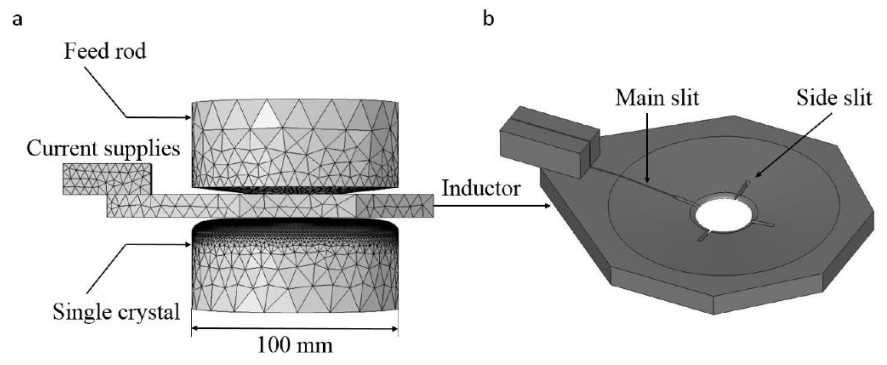
2. Numerical Models
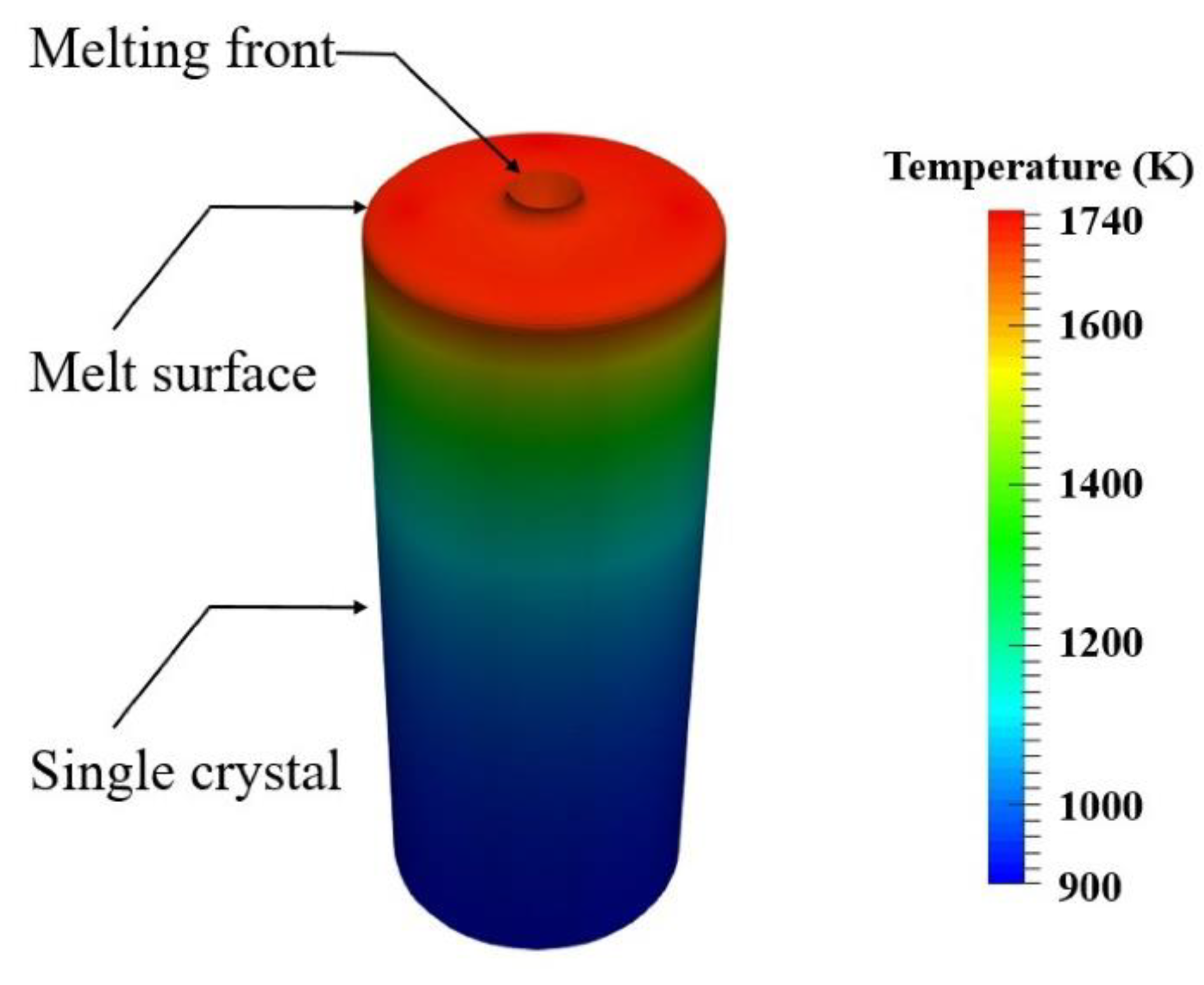
3. Results and Discussion
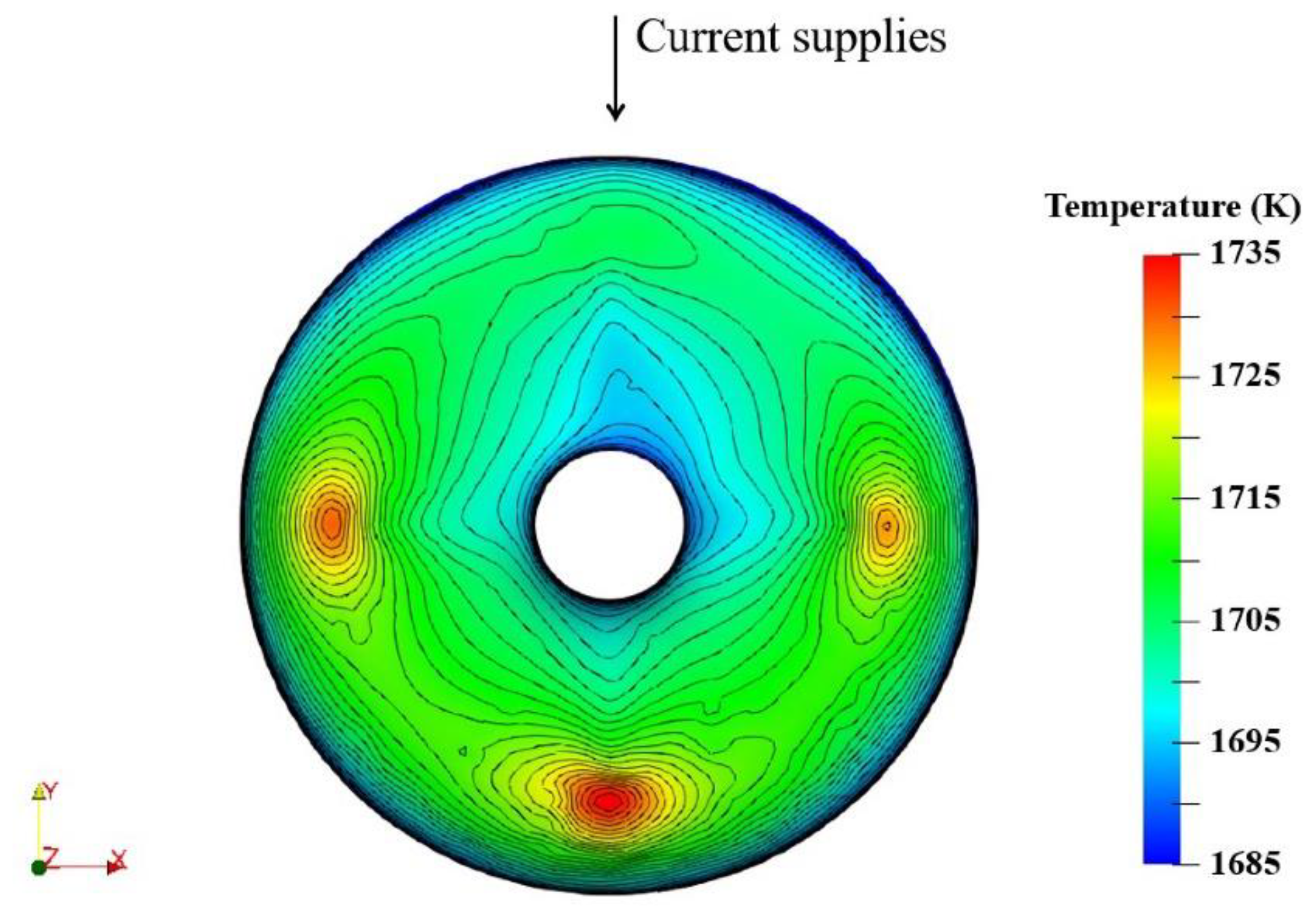
3.1. Current Density Analysis
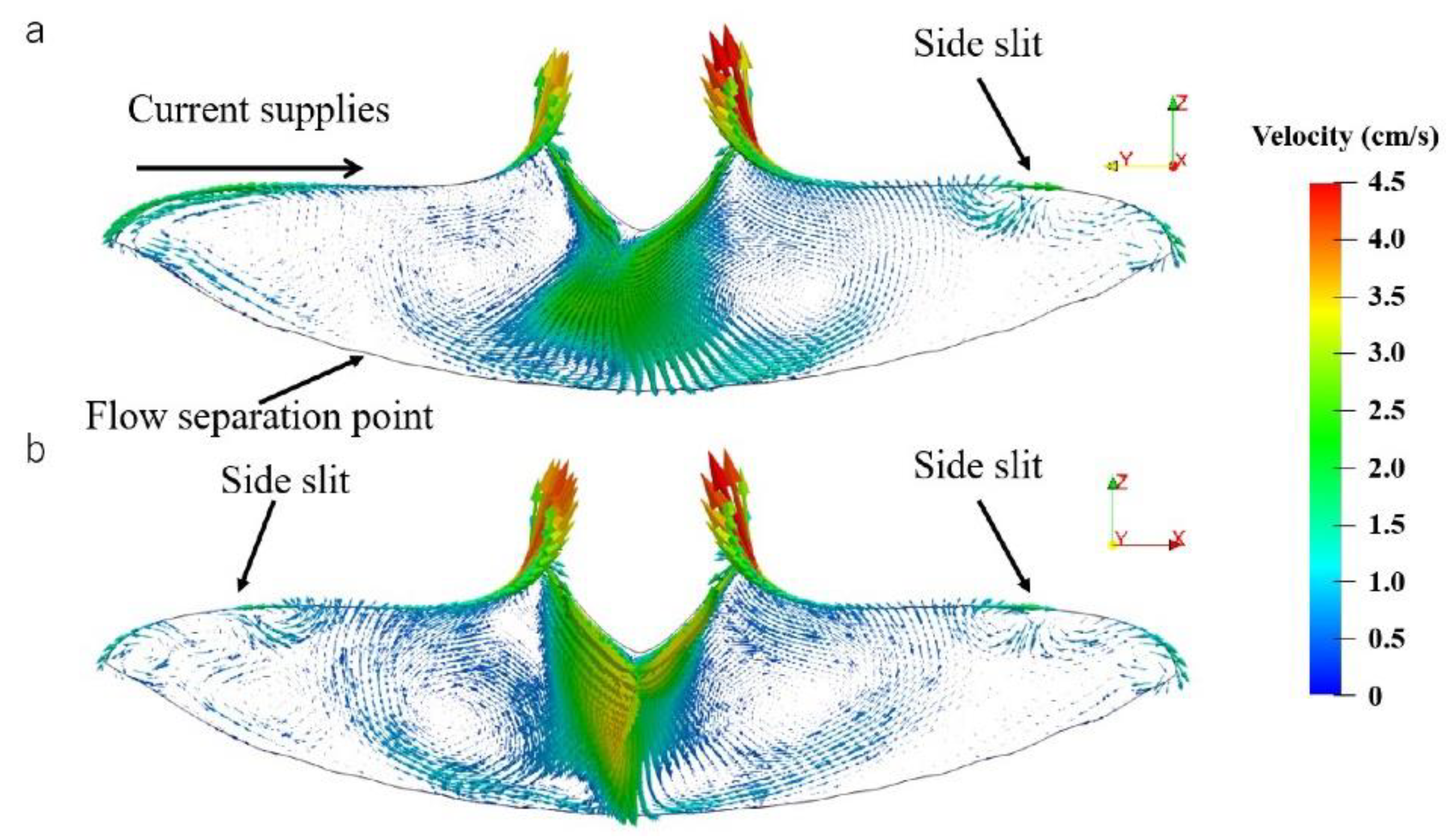
3.2. Melt Flow Analysis
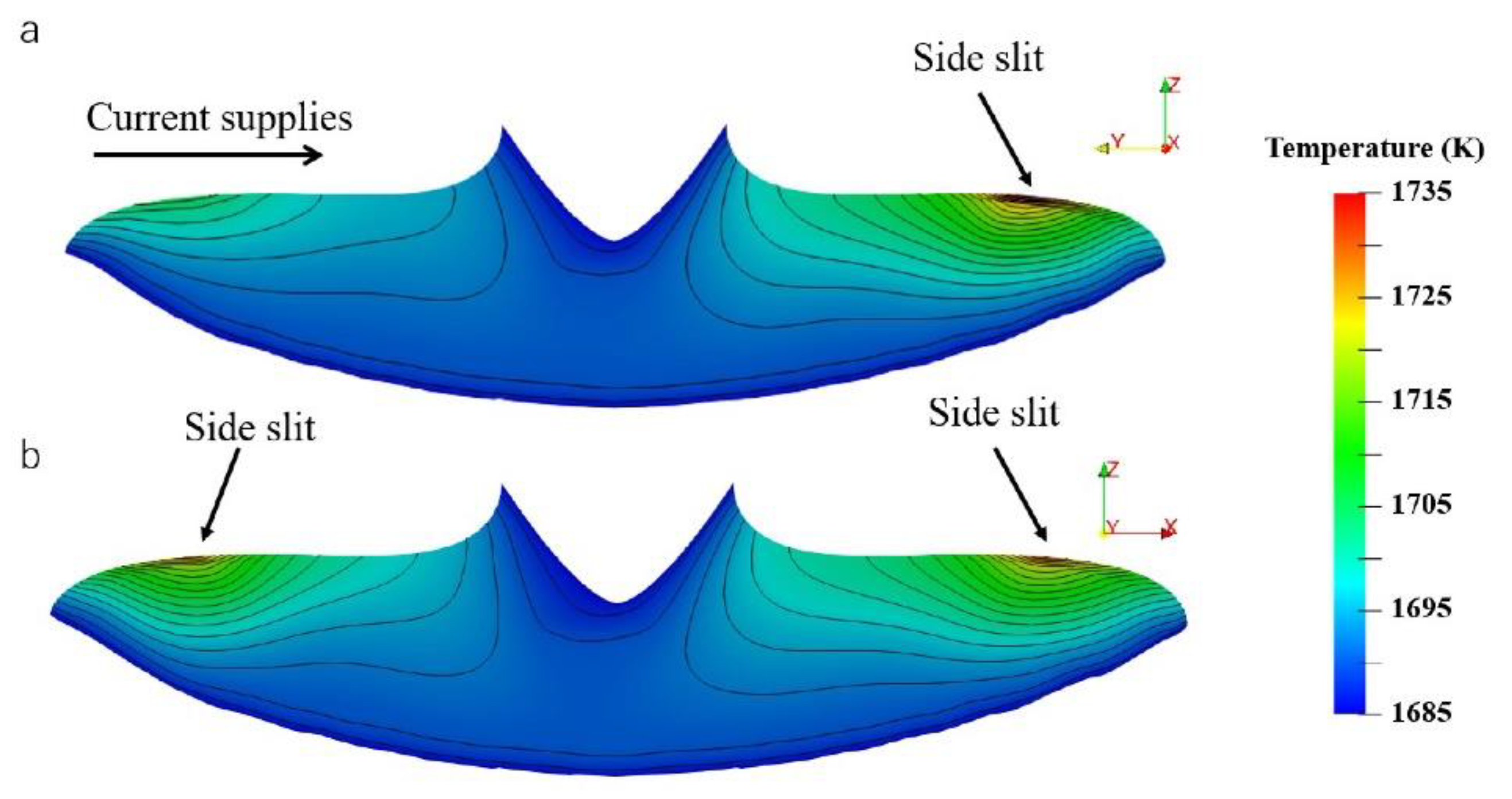
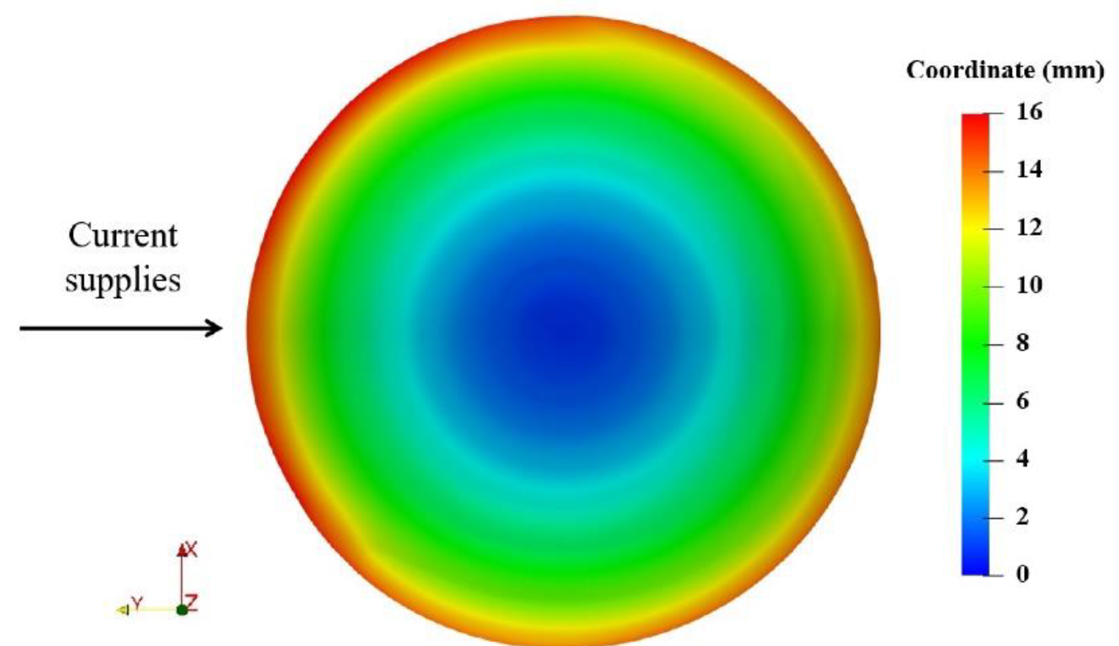
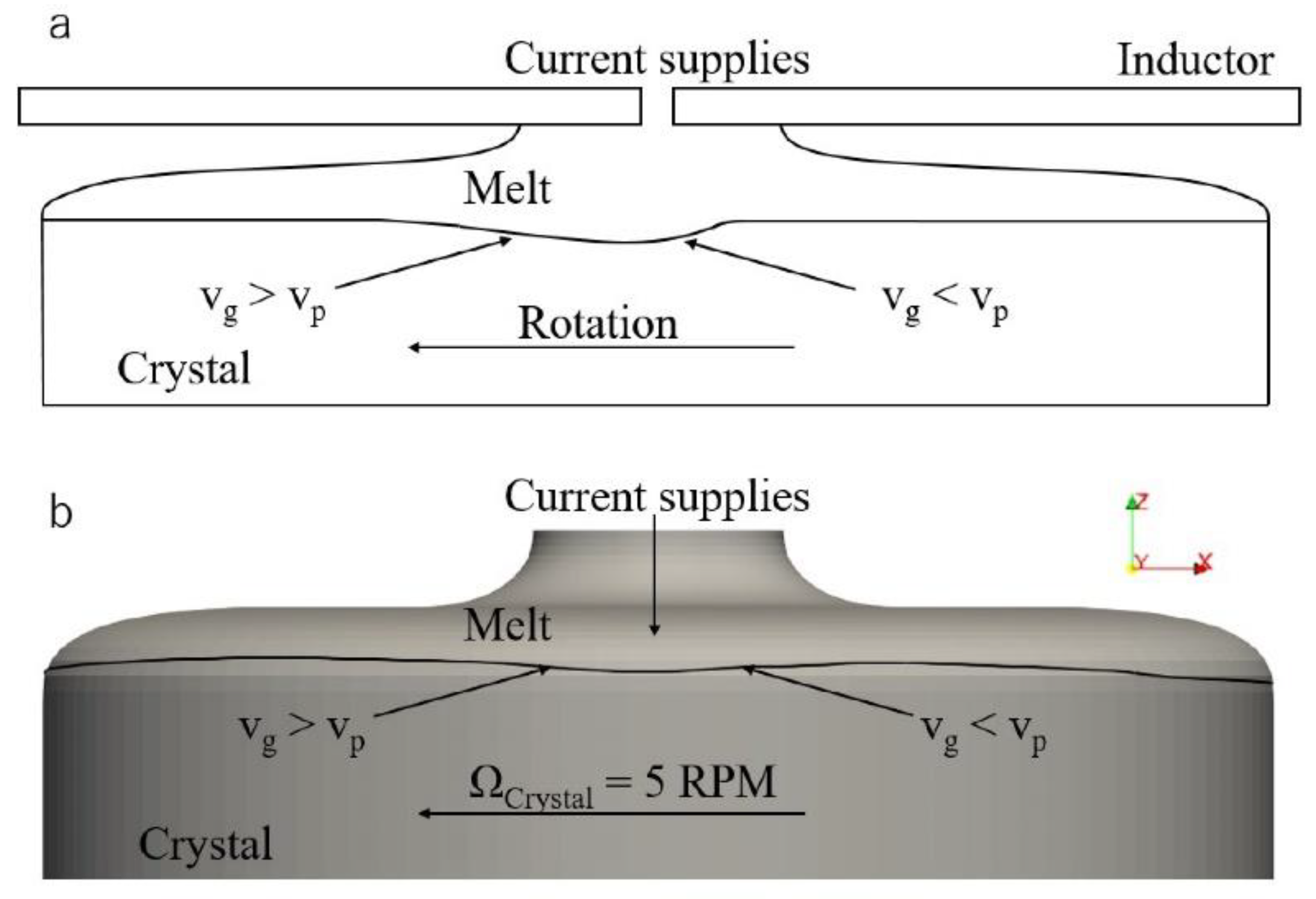
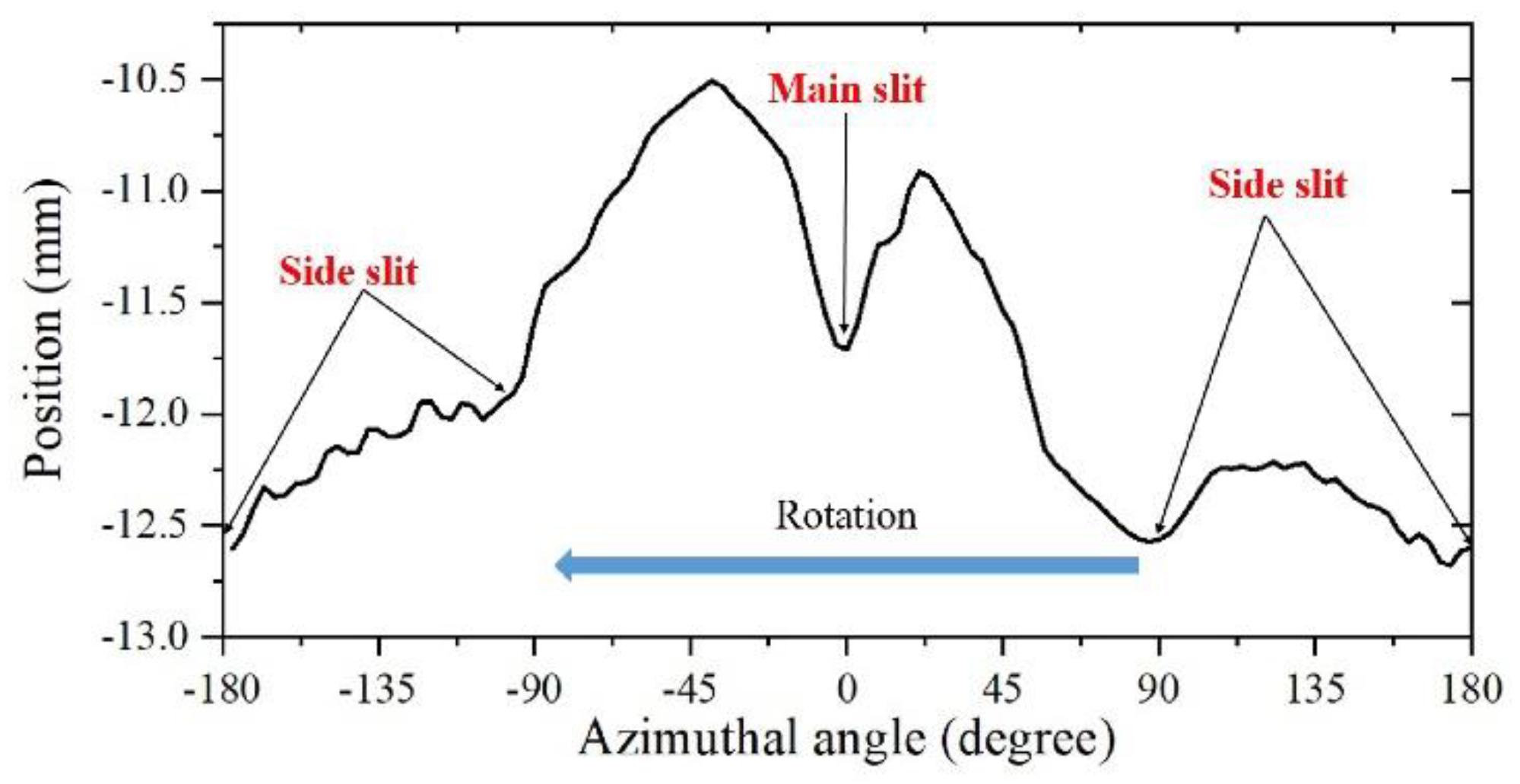
3.3. Three-Phase Line Analysis
4. Conclusions
Author Contributions
Funding
Conflicts of Interest
References
- Menzel, R. Growth Conditions for Large Diameter FZ Si Single Crystals. Ph.D. Thesis, Technical University of Berlin, Berlin, Germany, 2013. [Google Scholar]
- Mühlbauer, A.; Erdmann, W.; Keller, W. Electrodynamic convection in silicon floating zones. J. Cryst. Growth 1983, 64, 529–545. [Google Scholar] [CrossRef]
- Mühlbauer, A.; Muiznieks, A.; Virbulis, J.; Lüdge, A.; Riemann, H. Interface shape, heat transfer and fluid flow in the floating zone growth of large silicon crystals with the needle-eye technique. J. Cryst. Growth 1995, 151, 66–79. [Google Scholar] [CrossRef]
- Mühlbauer, A.; Muiznieks, A.; Raming, G.; Riemann, H.; Lüdge, A. Numerical modelling of the microscopic inhomogeneities during FZ silicon growth. J. Cryst. Growth 1999, 198, 107–113. [Google Scholar] [CrossRef]
- Wünscher, M.; Lüdge, A.; Riemann, H. Growth angle and melt meniscus of the RF-heated floating zone in silicon crystal growth. J. Cryst. Growth 2011, 314, 43–47. [Google Scholar] [CrossRef]
- Sabanskis, A.; Virbulis, J. Simulation of the influence of gas flow on melt convection and phase boundaries in FZ silicon single crystal growth. J. Cryst. Growth 2015, 417, 51–57. [Google Scholar] [CrossRef]
- Raming, G.; Muiznieks, A.; Mühlbauer, A. Numerical investigation of the influence of EM-fields on fluid motion and resistivity distribution during floating-zone growth of large silicon single crystals. J. Cryst. Growth 2001, 230, 108–117. [Google Scholar] [CrossRef]
- Ratnieks, G.; Muiznieks, A.; Mühlbauer, A.; Raming, G. Numerical 3D study of FZ growth: Dependence on growth parameters and melt instability. J. Cryst. Growth 2001, 230, 48–56. [Google Scholar] [CrossRef]
- Rudevics, A.; Muiznieks, A.; Ratnieks, G.; Riemann, H. 3D modeling of the molten zone shape created by an asymmetric HF EM field during the FZ crystal growth process. Magnetohydrodynamics 2005, 41, 123–146. [Google Scholar]
- Sabanskis, A.; Surovovs, K.; Virbulis, J. 3D modeling of doping from the atmosphere in floating zone silicon crystal growth. J. Cryst. Growth 2017, 457, 65–71. [Google Scholar] [CrossRef]
- Plāte, M.; Krauze, A.; Virbulis, J. Three-dimensional modelling of thermal stress in floating zone silicon crystal growth. In Proceedings of the IOP Conference Series: Materials Science and Engineering, Vanderbijlpark, South Africa, 23–26 October 2018; Volume 355, p. 012005. [Google Scholar]
- Plāte, M.; Krauze, A.; Virbulis, J. Mathematical modelling of the feed rod shape in floating zone silicon crystal growth. J. Cryst. Growth 2017, 457, 85–91. [Google Scholar] [CrossRef]
- Han, X.-F.; Liu, X.; Nakano, S.; Harada, H.; Miyamura, Y.; Kakimoto, K. 3D Global Heat Transfer Model on Floating Zone for Silicon Single Crystal Growth. Cryst. Res. Technol. 2018, 53, 1700246. [Google Scholar] [CrossRef]
- Kakimoto, K.; Liu, L. Analysis of local segregation of impurities at a silicon melt–crystal interface during crystal growth in transverse magnetic field-applied Czochralski method. J. Cryst. Growth 2009, 311, 2313–2316. [Google Scholar] [CrossRef]
- Ratnieks, G.; Muiznieks, A.; Buligins, L.; Raming, G.; Mühlbauer, A.; Lüdge, A.; Riemann, H. Influence of the three dimensionality of the HF electromagnetic field on resistivity variations in Si single crystals during FZ growth. J. Cryst. Growth 2000, 216, 204–219. [Google Scholar] [CrossRef]


| Properties | Value and Unit |
|---|---|
| High-frequency inductor current | 1000 A |
| Current frequency | 3 MHz |
| Skin depth of melt | 0.26 mm |
| Skin depth of crystal | 1.3 mm |
| Skin depth of high frequency inductor | 0.037 mm |
| Electrical conductivity of melt | 1.2 S/m |
| Electrical conductivity of crystal | 5 S/m |
| Electrical conductivity of high frequency inductor | 6 S/m |
| Properties | Value and Unit |
|---|---|
| Melt thermal conductivity | 67 W/(m∙K) |
| Crystal thermal conductivity | 98 − (9.43 ) T − (2.89 ) T2 W/(m∙K) |
| Heat capacity of silicon | 900 J/(kg∙K) |
| Melt density | 2420 kg/m3 |
| Crystal density | 2330 kg/m3 |
| Marangoni coefficient of melt | −1.0 N/ (m∙K) |
| Latent heat of silicon | 1.8 J/kg |
| Emissivity of melt | 0.27 |
| Emissivity of crystal | 0.46 |
| Crystal pulling rate | 3 mm/min |
| Crystal rotation speed | 5 RPM |
| Feed rod rotation speed | −20 RPM |
| Single crystal diameter | 100 mm |
© 2020 by the authors. Licensee MDPI, Basel, Switzerland. This article is an open access article distributed under the terms and conditions of the Creative Commons Attribution (CC BY) license (http://creativecommons.org/licenses/by/4.0/).
Share and Cite
Han, X.-F.; Liu, X.; Nakano, S.; Harada, H.; Miyamura, Y.; Kakimoto, K. 3D Numerical Analysis of the Asymmetric Three-Phase Line of Floating Zone for Silicon Crystal Growth. Crystals 2020, 10, 121. https://doi.org/10.3390/cryst10020121
Han X-F, Liu X, Nakano S, Harada H, Miyamura Y, Kakimoto K. 3D Numerical Analysis of the Asymmetric Three-Phase Line of Floating Zone for Silicon Crystal Growth. Crystals. 2020; 10(2):121. https://doi.org/10.3390/cryst10020121
Chicago/Turabian StyleHan, Xue-Feng, Xin Liu, Satoshi Nakano, Hirofumi Harada, Yoshiji Miyamura, and Koichi Kakimoto. 2020. "3D Numerical Analysis of the Asymmetric Three-Phase Line of Floating Zone for Silicon Crystal Growth" Crystals 10, no. 2: 121. https://doi.org/10.3390/cryst10020121
APA StyleHan, X.-F., Liu, X., Nakano, S., Harada, H., Miyamura, Y., & Kakimoto, K. (2020). 3D Numerical Analysis of the Asymmetric Three-Phase Line of Floating Zone for Silicon Crystal Growth. Crystals, 10(2), 121. https://doi.org/10.3390/cryst10020121