Article

The Impact of Interfacial Charge Trapping on the Reproducibility of Measurements of Silicon Carbide MOSFET Device Parameters

1
Institute for Microelectronics, TU Wien, 1040 Wien, Austria
2
Infineon Technologies AG, 85579 Neubiberg, Germany
3
CDL for Single-Defect Spectroscopy at the Institute for Microelectronics, TU Wien, 1040 Wien, Austria
4
Infineon Technologies Austria AG, 9500 Villach, Austria
*
Author to whom correspondence should be addressed.
Crystals 2020, 10(12), 1143; https://doi.org/10.3390/cryst10121143
Submission received: 6 November 2020 / Revised: 5 December 2020 / Accepted: 11 December 2020 / Published: 16 December 2020
(This article belongs to the Special Issue Robust Microelectronic Devices)

Abstract

:
Silicon carbide is an emerging material in the field of wide band gap semiconductor devices. Due to its high critical breakdown field and high thermal conductance, silicon carbide MOSFET devices are predestined for high-power applications. The concentration of defects with short capture and emission time constants is higher than in silicon technologies by orders of magnitude which introduces threshold voltage dynamics in the volt regime even on very short time scales. Measurements are heavily affected by timing of readouts and the applied gate voltage before and during the measurement. As a consequence, device parameter determination is not as reproducible as in the case of silicon technologies. Consequent challenges for engineers and researchers to measure device parameters have to be evaluated. In this study, we show how the threshold voltage of planar and trench silicon carbide MOSFET devices of several manufacturers react on short gate pulses of different lengths and voltages and how they influence the outcome of application-relevant pulsed current-voltage characteristics. Measurements are performed via a feedback loop allowing in-situ tracking of the threshold voltage with a measurement delay time of only 1 μ s . Device preconditioning, recently suggested to enable reproducible BTI measurements, is investigated in the context of device parameter determination by varying the voltage and the length of the preconditioning pulse.

Graphical Abstract

1. Introduction

Silicon carbide (SiC) is a promising wide band gap semiconductor material. Especially in power applications, 4H-SiC metal-oxide-semiconductor field-effect transistors (MOSFETs) exhibit advantages over comparable silicon (Si) technologies. Owing to its wide band gap of around 3.26 e V [1], the critical breakdown field of SiC power MOSFETs is around ten times higher than the one of Si devices [2]. Hence, SiC devices of the same voltage and on-state resistance class can be made considerably smaller than comparable Si-based devices, leading to reduced device capacitances and enabling higher switching frequencies at lower losses [3,4]. This dramatically reduces volume and weight of inductors, filter capacitors, cooling components and hence, total system costs. Operation at higher frequency, more flexible thermal capability, and robustness to hard commutation events make SiC MOSFETs particularly suited for high efficiency topologies and high density designs. The wide band gap nature of the semiconductor further allows device operation at very high operating temperatures [5], which makes SiC MOSFETs ideal candidates for harsh environments.
SiC power MOSFETs have already been manufactured by semiconductor companies for several years. Commercially available designs differ with regard to the crystal direction along the inversion channel. Vertical power MOSFETs, which employ a trench design, allow for a higher cell density on the wafer, show a higher channel mobility, but the manufacturing process is more complex. In contrast, their planar counterparts exhibit a lower channel mobility, as the crystal direction differs, the cell density is lower, but manufacturing is less complex [6,7]. Regarding device performance, SiC trench MOSFETs have the potential to show even lower switching and conduction losses than planar designs, leading to an increase in efficiency of applications [8].
Although the experience in manufacturing SiC devices has been growing continuously in recent years, device reliability is still one of the most important aspects under focus of research and development. Besides extrinsic defects in the gate oxide [9], bias temperature instability (BTI) is a topic that requires particular attention [10]. An applied gate voltage, that can be either positive or negative, leads to charge capture events in defects inside the SiO 2 gate insulator. These defects are either located deeper in the oxide, in the interfacial transition region, or directly at the interface between SiC and SiO 2 . Such trapping and detrapping events lead to a transient shift of the threshold voltage and can be described by first-order reactions [11]. A peculiarity of SiC MOSFETs compared to Si counterparts is the high concentration of defects with short capture and emission time constants of roughly 10 12 / c m 2 [12,13]. These defects transform the threshold voltage to a rather dynamic quantity under application conditions [14]. In contrast to Si devices, in which threshold voltage shifts appear only as a gradual long-term drift (classical BTI), the threshold voltage of SiC devices shows a very fast transient reaction to even very short gate pulses in the submicrosecond range.
Two of the most important parameters of power MOSFETs are the threshold voltage V th and the on-state resistance R DS , on . For Si based MOSFETs, it is common practice to measure these parameters with an accuracy and reproducibility of 10 m V and 1%, respectively. Most importantly, application- or reliability-engineers can easily check or reproduce the corresponding datasheet values. For SiC MOSFETs, measuring the threshold voltage and the on-state resistance is more complex. The short-term threshold voltage dynamics discussed above can be on the order of a few volts and arise even at very low gate voltages within very short times. These transient threshold voltage shifts have a negative influence on the reproducibility and comparability of measurements. New measurement procedures and their standardization, involving device preconditioning before readouts, are currently discussed [15,16,17].
At the moment, dedicated studies on the impact of the short-term dynamics of interfacial charge trapping on the reproducibility of device parameter measurements and investigations on differences between preconditioning pulses do not exist. In this study, we therefore characterize four different state-of-the-art commercially available SiC power MOSFETs from different vendors with regard to the charge trapping dynamics during current-voltage characteristics (IV-curve) measurements. It will be shown how these transient threshold voltage shifts quantitatively enter device parameters. Furthermore, we will examine the impact of preconditioning pulse length and bias variations on the reproducibility of threshold voltage readouts.

2. Materials and Methods

The employed commercially available SiC power MOSFETs are from four different vendors. For reasons of comparability, the MOSFETs have the same maximum voltage rating of 1200   V and comparable maximum gate-source voltage ratings. Furthermore, the typical on-state resistance is comparable and in the range of 160–500 m Ω at room temperature. The devices are arbitrarily labeled as A, B, C, and D, whereby A and B have a trench design and C and D are planar MOSFETs. Additional external gate resistors in series to the respective positive or negative voltage source enable defined transitions between two voltage levels of different polarity. The gate resistors are chosen to set the rise and fall times for a transition between 10   V and 20   V to 50   n s for all devices, which is typical for fast switching applications of 100   k Hz . Thereby, overshoots and undershoots are avoided. An overview of the different samples is found in Table 1.
All measurements are performed at room temperature with a homebuilt setup enabling excellent control over the performed measurement procedures and ultra-fast threshold voltage readouts [13,18], which are executed by forcing a drain-source current of 1   m A at a drain-source voltage of 1   V and by tracking the corresponding gate voltage via an operational amplifier based feedback loop. The setup allows measurement delay times down to 1   μ s .

3. Results

In this study, we define the threshold voltage as the gate voltage that is necessary to yield a certain drain-source current at a defined drain-source voltage. This allows its measurement by continuously forcing the chosen drain-source current via a feedback loop. As shown in Figure 1a, the resulting continuous application of the threshold voltage during a measurement leads to considerable shifts on the order of several hundred millivolts. The striking consequence is that charge trapping is present even at the comparably low threshold voltage that hence changes over time. Naturally, such effects also affect the drain-source current because a shift in the threshold voltage changes the gate voltage overdrive. This is especially visible in SiC MOSFETs when switching from negative to positive gate voltages (see Figure 1b). A similar effect can hardly be observed in Si devices (see inset Figure 1b).
As such drain-source current variations will of course arise during pulsed IV-curve measurements and thus influence the measured device parameters, we will investigate in the following the transient threshold voltage shift after short gate pulses and the drain-source current variations during pulsed IV-curves and finally correlate these two effects.

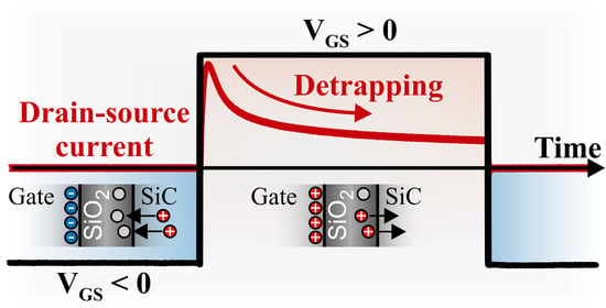
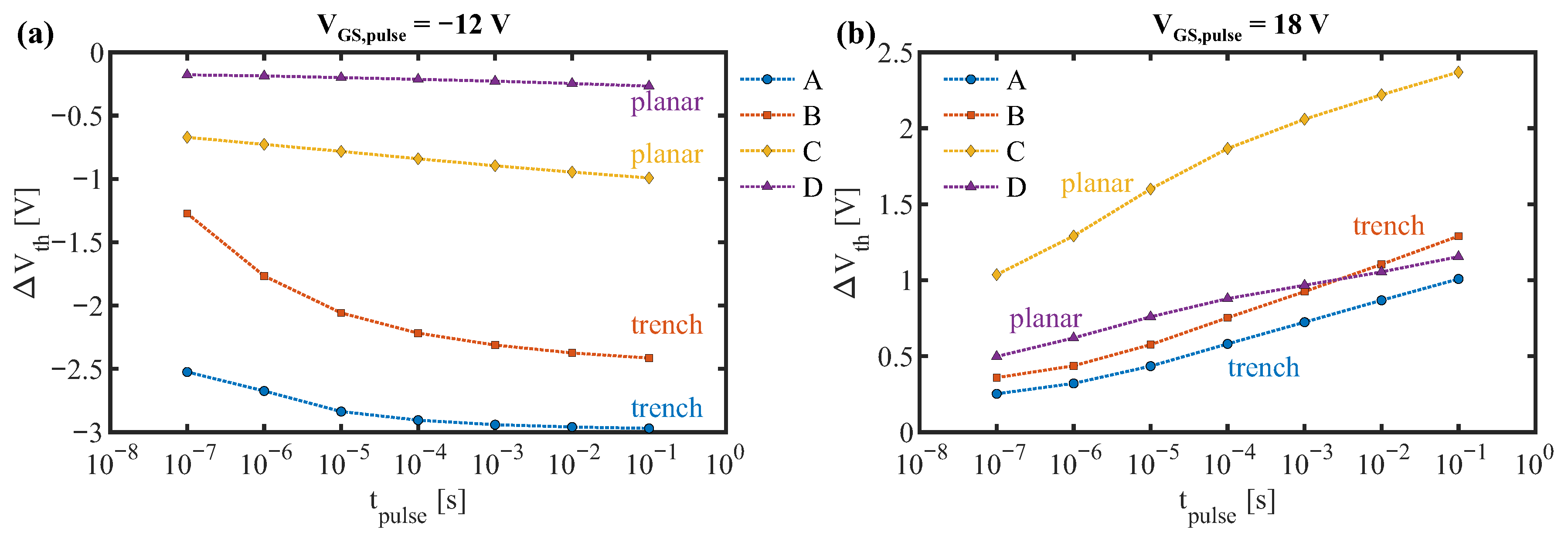
3.1. Threshold Voltage Dynamics after Short Gate Pulses

First, we determined the impact of short gate pulses of both positive and negative polarity on the threshold voltage. The measurement scheme is shown in the inset of Figure 2a. After a pulse of a certain length t pulse and voltage V GS , pulse had been applied to the gate, while keeping both drain and source contact grounded, the threshold voltage transients were measured for around 2   min via the feedback loop. Remember that during the recovery phase the threshold voltage is continuously applied to the gate. Finally, the shift of the threshold voltage is determined by comparing the value at a specific recovery time to the threshold voltage at the same recovery time in a measurement where no pulse had been applied before (see Figure 1a). Each measurement sequence, consisting of pulses of different lengths and voltages, is performed with the same device, whereby the single measurements are separated by additional recovery periods of 2   min with all terminals grounded. These additional recovery periods allow the device to return to its pristine state. Exemplary recovery traces from the described measurements are presented in Figure 2 for each device. All plots contain the threshold voltage shift recovery traces after positive and negative pulses of different lengths.
Based on these results, Figure 3 illustrates the dependence of the threshold voltage shift on the pulse length for the two shown pulse voltages, while keeping the recovery time constant at 1.8   μ s . Obviously, the longer the pulse length, the higher the absolute threshold voltage shift. However, note that for the negative voltage, the t pulse -dependence above 1   m s is rather weak. Regarding the design impact, the two planar devices show less transient threshold voltage shift after the negative pulse than the two trench devices. In contrast, the two trench devices vastly show less threshold voltage shift for the positive pulse, whereby the maximum transient shift is observed in the planar device C. Note that pulses of only 100   n s lead to a shift of the threshold voltage in the volt regime.
The same measurements, as presented in Figure 2, were performed for several other voltages yielding the pulse voltage dependence of the threshold voltage shift for the two pulse lengths 1   μ s and 100   m s respectively (see Figure 4). For positive pulse voltages, the behavior is similar for all devices. Regarding negative pulse voltages, the trench devices show a stronger pulse voltage dependence than the planar devices.
An obvious question is how long one has to wait after a pulse to come back to the original threshold voltage within a certain limit, which is shown in Figure 5. For a pulse length of 1   μ s and negative pulse voltages, the time can reach up to the order of 1–100 s at which there is still a remaining threshold voltage shift of 50   m V , even though the causing pulse length was several orders of magnitude shorter. For the highest positive pulse voltage, the time to reach the limit is lower. In comparison to longer pulses of 100   m s and a higher precision limit of 200   m V , the times are roughly on the same order. Interestingly, the tested trench devices reach the respective precision level for positive voltages faster than the planar devices.

3.2. Drain-Source Current Voltage Characteristics and On-State Resistance

In this section, we study the impact of interfacial charge trapping on IV-curves and device parameters. A short gate pulse of 70   μ s typically leads to a dissipated power P = V DS · I DS = 3 W resulting in a junction temperature increase of only 1   C . In order to avoid self-heating, all IV-curves are hence executed in a pulsed mode with sufficiently long off-state times. Commercial curve tracers pulse the drain-voltage while slowly sweeping the gate voltage. Although this technique works perfectly for Si-MOSFETs or IGBTs, it is devastating for SiC MOSFETs because in their case, this method would lead to a drastic increase in the threshold voltage during the sweep by more than 1   V (see Figure 4). The gate overdrive V GS V th would thus decrease. Hence, for SiC MOSFETs pulsing the drain bias has to be replaced by pulsing the gate. A long negative pulse at a base voltage has to be applied between the positive gate pulses in order to discharge all traps that had been charged during the preceding positive pulse and bring the electrically active defects in a defined charge state. Furthermore, pulsed IV-curves can be adapted to typical application conditions of SiC MOSFETs which are characterized by a pulsed gate-source voltage up to 100   k Hz . Thus, they provide application-relevant drain-source current measurement values.
Recalling Figure 1b, the measured drain-source current in pulsed IV-curves with a fixed drain-source voltage is influenced by four parameters: the base voltage V base , the length of the base pulse, the measurement delay t D , and the integration time t I . As the integration time can be interpreted as an average over different delay times, we do not consider its dependence here and choose a rather small integration time of 3.6   μ s compared to the pulse length of 70   μ s . The length of the base pulse is also kept constant at 1   m s because the threshold voltage shift after negative gate pulses is almost identical for all measured pulse lengths longer than 1   m s (see Figure 3a).
For a precise characterization of the drain-source current variations during pulsed IV-curves, we measured a series of them, whereby the base voltage V base was varied and the current was measured after different delay times. Figure 6 shows the difference in the IV-curve, the on-state resistance, and the transconductance for two different base voltages V base but at the same delay time. Obviously, a lower base voltage leads to an increased drain-source current. Deviations from a parallel shift of the IV-curve hint towards changes in the channel mobility. Though the influence of the base voltage is minimized for device D, as could be expected from low hole trapping at negative gate voltage (see Figure 4a), all devices are affected. This is in accordance with observations in previous literature [19]. The reduction in the on-state resistance reaches up to 20   m Ω (≈4%) for device A and even 34   m Ω (≈8%) for device C.
An illustration of the impact of the delay time on the drain-source current is shown in Figure 7, where two different delay times were used with the same base voltage. The observed change in the drain-source current is on the same order as the one that resulted from a change of the base voltage. Again, while the influence is minimized for device D, all devices show a significant change. Such a small difference in delay time of only 60   μ s already translates for device A into a shift of the maximum transconductance of a few hundred millivolt and a difference in the on-state resistance of up to 20   m Ω (≈5%) at a gate bias of 15   V . For device C, the difference even reaches 30   m Ω (≈8%).
For more insights, a detailed dependence of the change in the drain-source current on the base voltage is shown in Figure A2 for different delay times. We define the quantities Δ I DS t D and Δ I DS V base , as illustrated in Figure A2, to be the maximum observed change in the drain-source current due to a change in the delay time (relative to the lowest delay time) or the base voltage (relative to the lowest base voltage). The quantity Δ I DS V base of the tested devices ranges from 0.4% to 8.7%. With decreasing base voltage, the drain-source current increases monotonously for all devices except for device C. Here, the drain-source current shows a local minimum at 2   V . In this case, the evaluation relative to the minimum would lead to a variation in the drain-source current of over 10%. Due to its generally small current variations, device D is the only device showing noise in the change of the drain-source current. At a certain base voltage, that is different for each of the four tested devices, the change in the drain-source current saturates. The quantity Δ I DS t D is different for each device and ranges from 0.2% to 2.5%.
As observed in the measurements in Figure 2, the lower the pulse voltage and the longer the pulse, the larger is the absolute change of the threshold voltage and, thus, the larger is the change in the gate voltage overdrive leading to a higher drain-source current. As a result, the change in drain-source current correlates with the transient threshold voltage shift. In order to prove this correlation, drain-source current measurements with different delay times were plotted versus the observed change in the threshold voltage after a negative pulse that corresponds exactly to the off-state time and base voltage in the drain-source current measurement. The results are presented in the appendix in Figure A3. Pearson correlation coefficients indicate strong linear correlation near unity.

3.3. Device Preconditioning

Device preconditioning is often performed with either a negative accumulation pulse or a positive inversion pulse prior to drain-source current or threshold voltage measurements. Sometimes, both types of pulses are used consecutively. As discussed in the previous sections, any gate pulse, even the measurement itself, will cause an out-of-equilibrium state of the interfacial charge traps affecting the threshold voltage. For device reliability, stress tests where a threshold voltage shift is determined relative to a reference readout before applied device stress, it is sufficient to be able to create at each readout, including the reference readout, a defined out-of-equilibrium state. This is a very good approach as long as the timing and the voltages of the preconditioned measurement scheme are precisely kept constant and as long as the underlying degradation mechanism does not affect the transient threshold voltage shift [16,17]. However, an inaccurate recovery time between the end of the preconditioning pulse and the readout can have an impact on the precision and the reproducibility of the measurement. In cases where a defined recovery time cannot be provided, a close to equilibrium charge state of the involved traps has to be achieved before each measurement. In the following, we investigate this case with a negative accumulation pulse (see inset of Figure 8a). The idea is to remove trapped electrons with short time constants which can help to achieve reproducible measurements and to measure mainly application-relevant permanent drift components in long-term stress tests of positive gate bias. For this study, we chose a stress pulse of 1   s at 20   V . Such a stress pulse could typically arise during measurements of IV-curves or as an unintentional variation of the applied gate voltage before a threshold voltage readout in reliability tests. In order to reveal the impact of preconditioning pulses on the removal of the captured electrons, we executed measurements where preconditioning pulse voltage and length were varied. As the threshold voltage of device A is more sensitive to negative gate voltages than the one of the other devices, we limited the measurements to this device. Figure 8 shows the threshold voltage traces after stress and preconditioning. Each plot corresponds to one of four preconditioning voltages V prec , whereby the pulse length t prec was varied. The stress without preconditioning causes a transient shift of the threshold voltage of approximately 1   V . At a preconditioning voltage of 3   V , pulse lengths between 1 and 100 μ s reduce the transient shift already significantly. At a pulse length of 1   m s , an initially positive slope of the recovery trace indicates the emission of holes. However, for longer recovery times, the recovery is still dominated by the emission of electrons. The preconditioning pulse is already sufficient to change the sign of the threshold voltage shift, although the difference to the stress pulse is three orders of magnitude in time and the preconditioning voltage is relatively small. At a lower preconditioning voltage of 6   V , the threshold voltage shift is not only negative for all measured preconditioning pulse lengths, but the absolute value of the threshold voltage shift is even increased compared to the case of no preconditioning. Decreasing the preconditioning voltage even more results in gradually increasing absolute shifts of the threshold voltage, whereby the preconditioning pulse length looses its influence, as the different recovery traces merge.
This merging becomes particularly visible in Figure 9. It shows the dependence of the recovery time needed after preconditioning to return to a threshold voltage shift below 100   m V . To remove the influence on the threshold voltage of the applied positive pulse, a preconditioning pulse of 3   V for 1   m s appears to be a very good compromise. However, the impact on the needed recovery time of a small error in preconditioning time is considerably high at 1   m s , which would lead to poor reproducibility. For the lower preconditioning voltages, the required recovery time is almost the same, especially for longer preconditioning pulses. The necessary additional recovery time after preconditioning is around 440   m s . Without preconditioning, the required recovery time is approximately 20–30 s . Negative preconditioning can hence reduce the recovery time required to come back to the initial threshold voltage by around two orders of magnitude.

4. Discussion

Due to the extraordinarily wide distribution of capture time constants of defects in SiC devices, all presented measurements are heavily affected by charge trapping. Continuously measuring the threshold voltage via a feedback loop reveals the drastic time dependence of such measurements, during which the applied threshold voltage leads to electron capture events in the electrically active defects, resulting in return in a dynamic increase of the threshold voltage. Short-term charge trapping is inherent in all measurements, as it cannot be avoided due to measurement delays. The observed asymmetry between capture and emission times has already been investigated by means of capture and emission time maps [13], confirming the existence of defects with longer emission than capture time constants. The observation of hysteresis in swept IV-curves is a direct implication of this effect [12]. Furthermore, fast gate voltage up sweeps starting at different negative values are also affected (see Figure A1). As shown in Figure 1b, switching a SiC MOSFET from a negative to a positive gate bias results in a gradually decreasing drain-source current. This effect can be linked to charge trapping via the observed threshold voltage shift. During the time at negative gate bias, fast hole trapping, probably at the interface [12,20], leads to a negative shift of the threshold voltage (see Figure 2). This leads to an initially increased gate voltage overdrive and hence to a higher drain-source current. During the positive gate pulse, the trapped holes gradually get emitted which increases the threshold voltage again. As a result, the gate voltage overdrive and the drain-source current decrease. A strong linear correlation between the drain-source current and the threshold voltage shift undermines this mechanism (see Figure A3). Small deviations can be attributed to variations in the channel mobility and the influence of the difference in the positive gate voltage during threshold voltage measurement and drain-source current measurement.
This short-term response of the threshold voltage leads to difficulties regarding the reproducibility of device parameter measurements. At a high level of 15   V at the gate (see Figure A2), a modification of the base voltage can lead to a change in the drain-source current of almost 10%. Furthermore, an increase in delay time of only 60   μ s can reduce the drain-current by up to 2.5%. These variations propagate to other device parameters, such as transconductance and on-state resistance (see Figure 6 and Figure 7). Precise device parameter measurements have to take such variations into account and they have to be considered when comparing results from different measurement schemes or even different measurement setups. However, short-term threshold voltage shifts should not necessarily be considered as a detrimental property in most applications because these transient effects are fully reversible and therefore do not cause typical BTI-induced reliability issues.
Differences between tested devices can be explained by multiple factors. The crystal plane of the interface and manufacturing processes, such as post oxidation anneals, influence the atomic structure of the interface and hence the trapping dynamics of charge carriers.
In device characterization measurements or device reliability tests, it is often required to remove electrons with small emission time constants trapped during positive gate stress. The application of a negative preconditioning pulse prior to threshold voltage readouts does not only accelerate the emission of trapped electrons, but it also triggers the capture of holes. On short time scales, the impact of the negative preconditioning pulse quickly dominates the recovery behavior (see Figure 8). For our exemplary stress pulse, the emission of most electrons required up to 440   m s to get the absolute threshold voltage shift back below 100   m V resulting in an acceleration of recovery by around two orders of magnitude. Below 6   V , this was almost independent of the considered preconditioning pulse length and of the chosen preconditioning voltage. The reason for this advantageous behavior is that hole capture time constants of the electrically active defects become shorter than the used pulse lengths.

5. Conclusions

In summary, we have presented the short-term charge trapping dynamics in SiC MOSFETs of several manufacturers and linked them via the impact on the threshold voltage to the drain-source current variations during pulsed IV-curve measurements. Our results clearly show that device parameters, such as threshold voltage, drain-source current, and on-state resistance, strongly depend on the measurement scheme and precise timing on a microsecond scale. The value of such parameters is influenced by the measurement procedure itself and the short- and long-term history of the gate signal. Without precise timing, the error of a measured on-state resistance is around 10% and without the use of any preconditioning techniques, the error of the threshold voltage can reach several volts.
Furthermore, negative preconditioning is a very effective and tolerant approach for the accelerated removal of trapped electrons with small time constants. Fast recovery of holes trapped during the preconditioning pulse and the insensibility to the preconditioning parameters are major advantages of this method. It has to be emphasized that every measurement following preconditioning is however again strongly dependent on its measurement parameters.

Author Contributions

Conceptualization, T.G. and H.R.; methodology, H.R.; investigation, M.W.F., A.H., K.P. and C.S.; writing—original draft preparation, M.W.F.; writing—review and editing, M.W.F., A.H., K.P., C.S., T.A., H.R. and T.G.; visualization, M.W.F.; supervision, T.G. and W.G.; project administration, H.R. and T.A. All authors have read and agreed to the published version of the manuscript.

Funding

Open Access Funding by TU Wien Bibliothek.

Acknowledgments

The financial support by the Austrian Federal Ministry for Digital and Economic Affairs and the National Foundation for Research, Technology and Development is gratefully acknowledged. Furthermore, the authors acknowledge TU Wien Bibliothek for financial support through its Open Access Funding Programme.

Conflicts of Interest

The authors declare no conflict of interest.

Abbreviations

The following abbreviations are used in this manuscript:
SiCsilicon carbide
Sisilicon
MOSFETmetal-oxide-semiconductor field-effect transistor
BTIbias temperature instability

Appendix A. Sweeped IV-Curves at High Drain-Source Voltage

Figure A1. Fast gate voltage sweeps from different initial gate voltages up to 15   V within 5   μ s at a drain-source voltage of 800   V at 25   C and the corresponding smoothed data lines based on robust local regression smoothing (RLRS). While the IV-curves of the initial sweep voltages 0   V and 3   V coincide, the IV-curves corresponding to voltages of 5   V and 7   V are shifted towards lower gate voltages indicating a transient threshold voltage shift.
Crystals 10 01143 g0a1

Appendix B. Base Voltage Dependence of the Drain-Source Current

Figure A2. The normalized change of the drain-source current I DS for different delay times t D of (a) device A, (b) device B, (c) device C, and (d) device D. The quantities Δ I DS t D and Δ I DS V base describe the maximum induced change in the drain-source current, whereby the former describes the change due to increasing the delay time of 7   μ s and the latter expresses the change due to lowering the base voltage relatively to 0.25   V .
Crystals 10 01143 g0a2

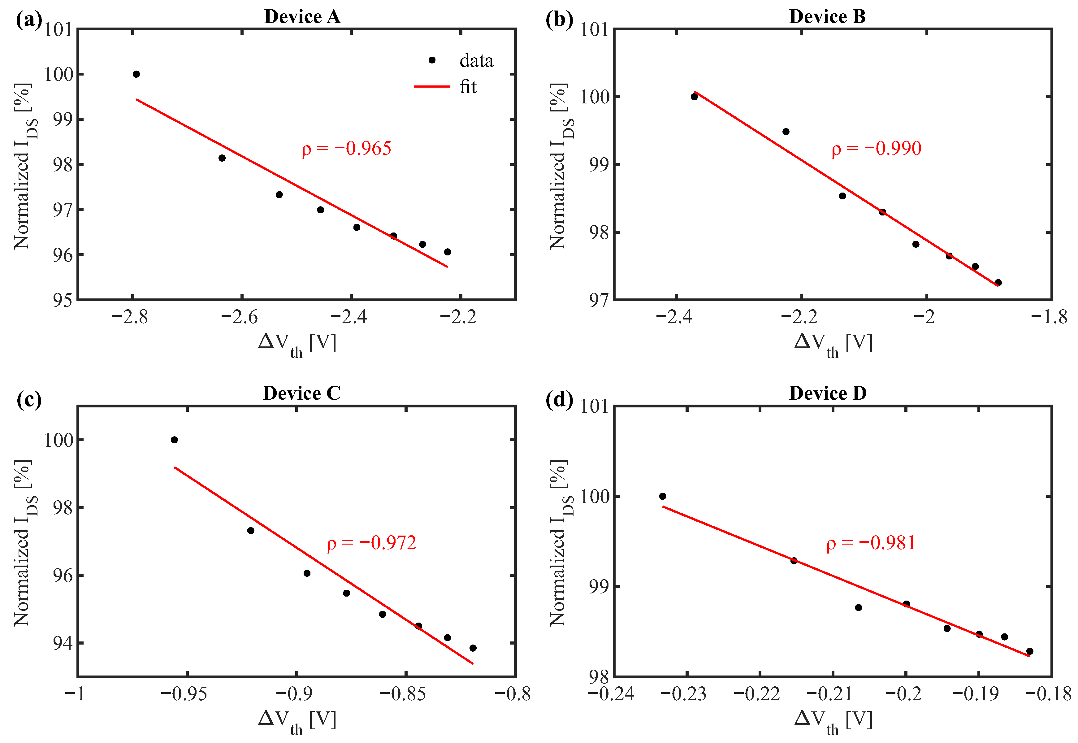
Appendix C. Correlation between Change in Drain-Source Current and the Threshold Voltage Shift

Figure A3. Correlation between the measured change in drain-source current normalized to the first readout and the threshold voltage shift during a 15   V pulse with a base voltage of 12   V . The red lines indicate linear fits. The shown quantity ρ is the Pearson correlation coefficient indicating strong linear correlation for all devices. The subfigures (a)–(d) correspond to the respective devices A–D. For the condition V DS V GS V th , the drain-source current follows I DS V GS V th , implying a linear relationship between the drain-source current and the threshold voltage shift. As the data satisfies both the condition and the linear relationship, it can be concluded that the observed change of the drain-source current indeed originates from the transient threshold voltage shift.
Crystals 10 01143 g0a3

References

  1. Afanas’ev, V.V.; Bassler, M.; Pensl, G.; Schulz, M.J.; Stein von Kamienski, E. Band offsets and electronic structure of SiC/SiO2 interfaces. J. Appl. Phys. 1996, 79, 3108–3114. [Google Scholar] [CrossRef]
  2. Palmour, J.W. Silicon carbide power device development for industrial markets. In Proceedings of the 2014 IEEE International Electron Devices Meeting, San Francisco, CA, USA, 15–17 December 2014; pp. 1.1.1–1.1.8. [Google Scholar] [CrossRef]
  3. Heer, D.; Domes, D.; Peters, D. Switching performance of a 1200 V SiC-Trench-MOSFET in a low-power module. In Proceedings of the PCIM Europe 2016, Nuremberg, Germany, 10–12 May 2016; pp. 53–59. [Google Scholar]
  4. Guo, S.; Zhang, L.; Lei, Y.; Li, X.; Xue, F.; Yu, W.; Huang, A.Q. 3.38 Mhz operation of 1.2kV SiC MOSFET with integrated ultra-fast gate drive. In Proceedings of the 3rd IEEE Workshop on Wide Bandgap Power Devices and Applications, Blacksburg, VA, USA, 2–4 November 2015; Volume 25, pp. 390–395. [Google Scholar] [CrossRef]
  5. Millan, J.; Godignon, P.; Perpina, X.; Perez-Tomas, A.; Rebollo, J. A Survey of Wide Bandgap Power Semiconductor Devices. IEEE Trans. Power Electron. 2014, 29, 2155–2163. [Google Scholar] [CrossRef]
  6. Peters, D.; Siemieniec, R.; Aichinger, T.; Basler, T.; Esteve, R.; Bergner, W.; Kueck, D. Performance and Ruggedness of 1200 V SiC-Trench-MOSFET. In Proceedings of the 2017 29th International Symposium on Power Semiconductor Devices and IC’s, Sapporo, Japan, 28 May–1 June 2017; pp. 239–242. [Google Scholar] [CrossRef]
  7. Yano, H.; Nakao, H.; Hatayama, T.; Uraoka, Y.; Fuyuki, T. Increased Channel Mobility in 4H-SiC UMOSFETs Using On-Axis Substrates. Mater. Sci. Forum 2007, 556–557, 807–810. [Google Scholar] [CrossRef]
  8. Anwar, S.; Wang, Z.J.; Chinthavali, M. Characterization and Comparison of Trench and Planar Silicon Carbide (SiC) MOSFET at Different Temperatures. In Proceedings of the 2018 IEEE Transportation Electrification Conference and Expo (ITEC), Long Beach, CA, USA, 13–15 June 2018; pp. 1039–1045. [Google Scholar] [CrossRef]
  9. Aichinger, T.; Schmidt, M. Gate-oxide reliability and failure-rate reduction of industrial SiC MOSFETs. In Proceedings of the 2020 IEEE International Reliability Physics Symposium (IRPS), Dallas, TX, USA, 28 April–30 May 2020; pp. 1–6. [Google Scholar] [CrossRef]
  10. Puschkarsky, K.; Grasser, T.; Aichinger, T.; Gustin, W.; Reisinger, H. Review on SiC MOSFETs High-Voltage Device Reliability Focusing on Threshold Voltage Instability. IEEE Trans. Electron. Devices 2019, 66, 4604–4616. [Google Scholar] [CrossRef]
  11. Schleich, C.; Berens, J.; Rzepa, G.; Pobegen, G.; Rescher, G.; Tyaginov, S.; Grasser, T.; Waltl, M. Physical Modeling of Bias Temperature Instabilities in SiC MOSFETs. In Proceedings of the 2019 IEEE International Electron Devices Meeting (IEDM), San Francisco, CA, USA, 7–11 December 2019; pp. 486–489. [Google Scholar] [CrossRef]
  12. Rescher, G.; Pobegen, G.; Aichinger, T.; Grasser, T. On the subthreshold drain current sweep hysteresis of 4H-SiC nMOSFETs. In Proceedings of the 2016 IEEE International Electron Devices Meeting (IEDM), San Francisco, CA, USA, 3–7 December 2016; pp. 10.8.1–10.8.4. [Google Scholar] [CrossRef]
  13. Puschkarsky, K.; Grasser, T.; Aichinger, T.; Gustin, W.; Reisinger, H. Understanding and Modeling Transient Threshold Voltage Instabilities in SiC MOSFETs. In Proceedings of the 2018 IEEE International Reliability Physics Symposium (IRPS), Burlingame, CA, USA, 11–15 March 2018; pp. 3B.5-1–3B.5-10. [Google Scholar] [CrossRef]
  14. Puschkarsky, K.; Reisinger, H.; Aichinger, T.; Gustin, W.; Grasser, T. Threshold voltage hysteresis in SiC MOSFETs and its impact on circuit operation. In Proceedings of the 2017 IEEE International Integrated Reliability Workshop (IIRW), Fallen Leaf Lake, CA, USA, 8–12 October 2017. [Google Scholar] [CrossRef] [Green Version]
  15. Lelis, A.J.; Green, R.; Habersat, D.B. SiC MOSFET threshold-stability issues. Mater. Sci. Semicond. Process. 2018, 78, 32–37. [Google Scholar] [CrossRef]
  16. Aichinger, T.; Rescher, G.; Pobegen, G. Threshold voltage peculiarities and bias temperature instabilities of SiC MOSFETs. Microelectron. Reliab. 2018, 80, 68–78. [Google Scholar] [CrossRef]
  17. Rescher, G.; Pobegen, G.; Aichinger, T.; Grasser, T. Preconditioned BTI on 4H-SiC: Proposal for a Nearly Delay Time-Independent Measurement Technique. IEEE Trans. Electron Devices 2018, 65, 1419–1426. [Google Scholar] [CrossRef]
  18. Reisinger, H.; Blank, O.; Heinrigs, W.; Mühlhoff, A.; Gustin, W.; Schlünder, C. Analysis of NBTI Degradation- and Recovery-Behavior Based on Ultra Fast VT-Measurements. In Proceedings of the 2006 IEEE International Reliability Physics Symposium Proceedings, San Jose, CA, USA, 26–30 March 2006; pp. 448–453. [Google Scholar] [CrossRef]
  19. Basler, T.; Heer, D.; Peters, D.; Aichinger, T.; Schörner, R. Practical Aspects and Body Diode Robustness of a 1200 V SiC Trench MOSFET. In Proceedings of the PCIM Europe 2018, International Exhibition and Conference for Power Electronics, Intelligent Motion, Renewable Energy and Energy Management. VDE, Nuremberg, Germany, 5–7 June 2018; pp. 536–542. [Google Scholar]
  20. Gruber, G.; Cottom, J.; Meszaros, R.; Koch, M.; Pobegen, G.; Aichinger, T.; Peters, D.; Hadley, P. Electrically detected magnetic resonance of carbon dangling bonds at the Si-face 4H-SiC/SiO2 interface. J. Appl. Phys. 2018, 123, 161514. [Google Scholar] [CrossRef] [Green Version]
Figure 1. (a) The shift of the threshold voltage during a measurement over time of all devices A–D. Note that the threshold voltage is continuously applied to the gate (constant I DS = 1   m A ) triggering electron trapping. (b) Gate signal of a 70   μ s pulse from V base = 12   V to V high = 6   V and a signal proportional to the corresponding drain-source current. Arrows indicate the measurement delay time t D and the integration time t I exemplarily for one out of several readouts. The current signal decreases monotonously during the pulse. The inset shows the same for a silicon MOSFET for comparison, where this effect is negligible.
Crystals 10 01143 g001
Figure 2. The recovery traces of the threshold voltage shift, respectively after a positive 18   V ( Δ V th > 0 ) or a negative 12   V ( Δ V th < 0 ) gate pulse. The pulse length t pulse was varied between 100   n s and 100   m s . The subfigures (ad) correspond to the respective devices A–D. The inset in (a) illustrates the measurement scheme consisting of an exemplary negative pulse followed by a continuous measurement of the threshold voltage.
Crystals 10 01143 g002
Figure 3. The pulse length dependence of the threshold voltage shift at the shortest measured recovery time of 1.8   μ s of the tested devices A–D for the two pulse voltages of (a) 12   V and (b) 18   V . The full data set is shown in Figure 2.
Crystals 10 01143 g003
Figure 4. The pulse voltage dependence of the threshold voltage shift at the shortest measured recovery time of 1.8   μ s of the tested devices A–D for the two pulse lengths (a) 1   μ s and (b) 100   m s . The full data set is shown in Figure 2.
Crystals 10 01143 g004
Figure 5. The recovery time necessary to reach a threshold voltage shift lower than a certain limit in dependence on the pulse voltage for a pulse length of (a) 1   μ s , a limit of 50   m V and for a pulse length of (b) 100   m s and a limit of 200   m V . The full data set is shown in Figure 2.
Crystals 10 01143 g005
Figure 6. The drain-source current I DS , transconductance g m and on-state resistance R DS , on for a measurement delay of 7   μ s and two different base voltages V base with an off-state time of 1   m s . The subfigures (ad) correspond to the respective devices A–D. The drain-source voltage V DS was set to 1   V , except for device B ( V DS = 0.5   V ). A lower base voltage yields a higher drain-source current.
Crystals 10 01143 g006
Figure 7. The drain-source current I DS , transconductance g m , and on-state resistance R DS , on for a base voltage of of 14   V and two different delay times t D with an off-state time of 1   m s . The subfigures (ad) correspond to the respective devices A–D. The drain-source voltage V DS was set to 1   V , except for device B ( V DS = 0.5   V ). A longer delay time yields a lower drain-source current.
Crystals 10 01143 g007
Figure 8. The recovery traces of the threshold voltage shift without preconditioning ( 0   s ) and with preconditioning pulses of lengths between 1   μ s and 10   s measured with device A. The subfigures (ad) correspond to different preconditioning voltages V prec between 3   V and 12   V . The inset in (a) illustrates the measurement scheme consisting of the stress pulse ( 20   V for 1   s ) followed by the preconditiong pulse. Except for the case of the 3   V preconditioning with pulse lengths between 1   μ s and 100   μ s , all preconditioning pulses are strong enough to change the sign of the threshold voltage shift.
Crystals 10 01143 g008
Figure 9. Required recovery time after preconditioning to return to a threshold voltage shift below 100   m V as a function of the preconditioning time. The raw measurement data is shown in Figure 8.
Crystals 10 01143 g009
Table 1. Overview of selected datasheet values and properties of the four different devices. The shown quantities are the maximum drain-source voltage V ( BR ) DSS , the threshold voltage V th , the minimum and maximum gate-source voltage ratings V GS , min and V GS , max , the input capacitance C iss , the design type, and a figure of merit.
Label V ( BR ) DSS [V] V th [V] V GS , min [V] V GS , max [V] C iss [pF]Design C iss R DS , on 1 [ns 1 ]
A12003.5–5.7−723182trench16
B12002.7–5.6−422398trench16
C12001.8–N/A−1025290planar7
D12002.0–4.0−1025259planar14
Publisher’s Note: MDPI stays neutral with regard to jurisdictional claims in published maps and institutional affiliations.

