Article

TCAD Simulation Study of ESD Behavior of InGaAs/InP Heterojunction Tunnel FETs

1
Integrated Circuit Reliability Design and ESD Protection Lab, School of Information Engineering, Zhengzhou University, Zhengzhou 450001, China
2
Shaanxi Key Laboratory of Complex System Control and Intelligent Information Processing, Xi’an University of Technology, Xi’an 710048, China
*
Author to whom correspondence should be addressed.
Crystals 2020, 10(11), 1059; https://doi.org/10.3390/cryst10111059
Submission received: 23 September 2020 / Revised: 15 November 2020 / Accepted: 19 November 2020 / Published: 21 November 2020

Abstract

:
For the first time, we investigated the electrostatic discharge (ESD) behavior of an InGaAs/InP heterojunction tunneling field effect transistor (HTFET). The device structure in this study has a high on-state current without extra process steps. Under the positive transmission line pulse (TLP) simulation, the band-to-band tunneling (BTBT) current acts as an important initial current to accelerate the occurrence of impact ionization and the device is turned on quickly. Under the negative transmission line pulse (TLP) simulation, the operating principle of the HTFET is the same as for a poly-bounded diode. The ESD robustness of the device under TLP simulation are evaluated, and the impact factors, with regard to ESD robustness and failure mode, are discussed. Finally, the device behavior under very fast transmission line pulse (VFTLP) simulations with different rise times and pulse widths is also investigated. The results show that this device may be used for the ESD protection of next-generation III–V technology.

1. Introduction

The phenomenon of band-to-band tunneling (BTBT) in tunnel field effect transistors (TFETs) enables them to achieve a subthreshold swing (SS) below 60 mV/dec at room temperature. TFETs have the potential to replace metal-oxide-semiconductor field effect transistors (MOSFETs) in next-generation integrated circuits [1,2,3]. Over the last decade, several device structures and materials, such as Si, Ge, SiGe, and III–V materials, have been proposed to fabricate TFETs with a high on-current (Ion) and low SS [4,5,6,7]. Among these material systems, In0.53Ga0.47As/InP heterojunction TFETs have a higher Ion/Ioff ratio compared to TFETs that are based on silicon in low-voltage applications because of the small lattice mismatch, small direct energy bandgap, and small tunneling mass [8,9]. Electrostatic discharge (ESD) is one of the key reliability issues of integrated circuits (ICs), especially in nanoscale technologies [10,11]. Recently, TFETs, which are based on silicon and SiGe as ESD protection devices, were investigated [12,13,14,15]. However, the electrostatic-discharge capacity of TFETs limits their application as ESD devices. They can, however, replace the traditional reverse diode as a secondary discharge device to reduce the clamp voltage and enhance the ESD robustness of the whole-chip protection network [16]. In addition, the breakdown voltage of the gate-oxide decreases with decreasing thickness [10], which is necessary to search for a potential device with lower trigger voltage. Therefore, InGaAs/InP heterojunction tunneling field effect transistor (HTFET) are promising candidates for ESD protection devices using the corresponding technology.
In this paper, the direct-current (DC) and ESD characteristics of InGaAs/InP HTFETs are investigated using a technology computer aided design (TCAD) simulation. The impact of device parameters, such as doping concentration, channel length, and junction depth, on BTBT generation and on-state current is explored. Transmission line pulse (TLP) simulations are conducted and show that InGaAs/InP HTFETs have a low trigger-voltage under positive stress, which makes them suitable for future low-voltage ICs. Under negative TLP, InGaAs/InP HTFETs operate like poly-bounded diodes and can conduct a high current. Finally, the very fast TLP (VFTLP) characteristic of the InGaAs/InP HTFET is also discussed.

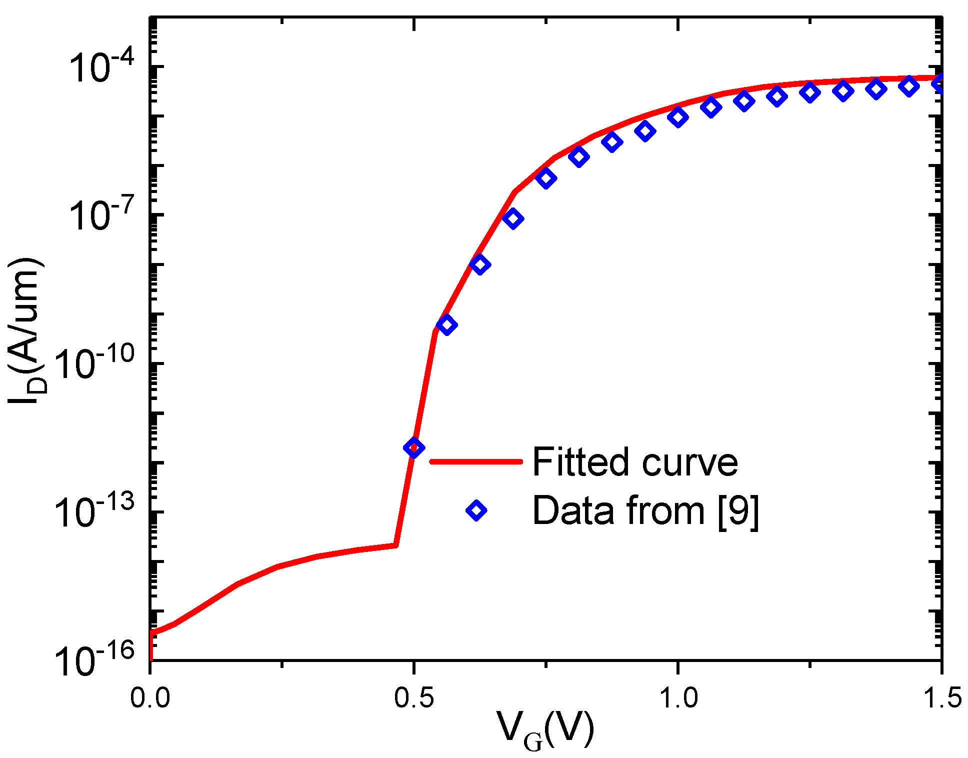
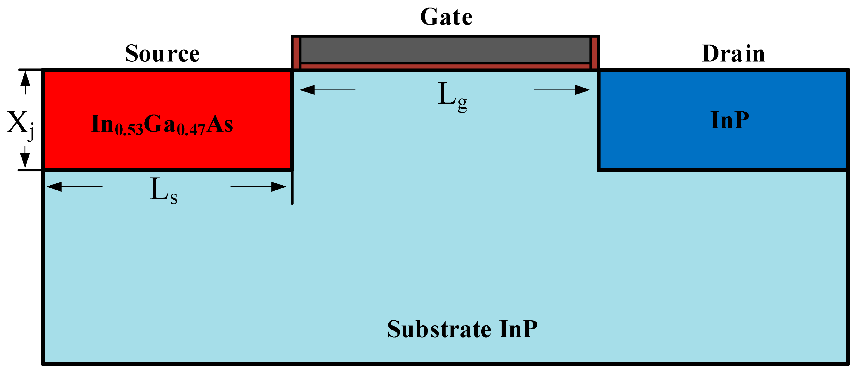
2. Model Calibration and Device Structure

The simulations for this work were performed using the Sentaurus-TCAD tool. We used the non-local dynamic BTBT model, the van Overstraeten–de Man avalanche-generation model, the high-field saturation model, the Philips unified mobility model, the thermionic emission model, band-gap narrowing, and the Shockley–Read–Hall recombination model. The quantum confinement has an insignificant impact when the device size is larger than 7 nm, and in turn was not considered in this paper [17,18]. The parameters that were used in this study were calibrated according to [7,9], and detailed values of the band structure are shown Table 1. A good match between the published data and our simulated result was obtained, as shown in Figure 1.
An HTFET structure was designed with In0.53Ga0.47As as a source material and InP as a substrate and drain material. The cross section of the device is shown in Figure 2. A metal gate (work function = 4.6 eV) with an HfO2 of 3 nm was used as a gate stack throughout the simulation. The doping concentrations of the source (P-type), drain (N-Type), and substrate (N-Type) were kept at 1 × 1019 cm−3, 1 × 1019 cm−3, and 1 × 1017 cm−3, respectively. The lengths of the source, channel, and drain were all set to 50 nm. Finally, the depth of the junction was set to Xj = 20 nm.

3. Off- and On-State Current with Different Parameters

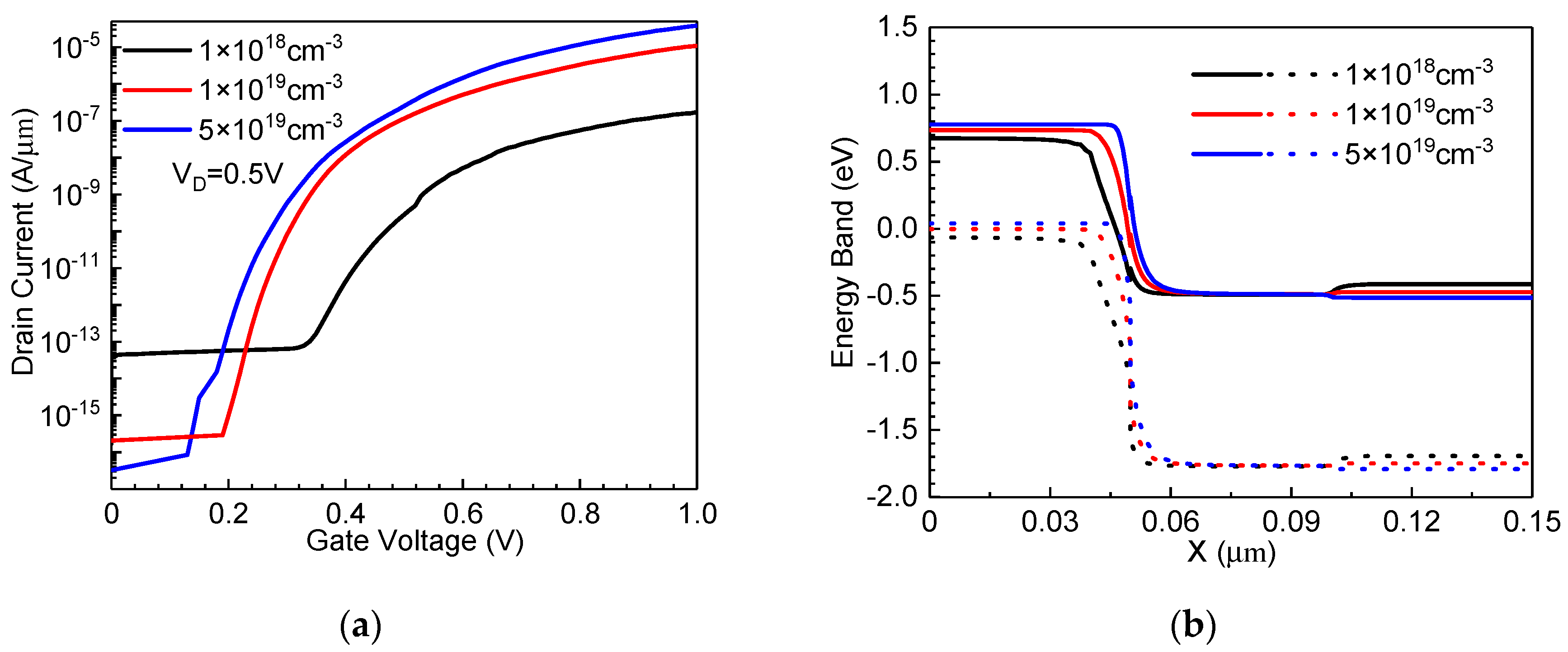
3.1. Effect of the Source Doping Concentration

Figure 3a shows that when the doping concentration in the source region is increased (while other parameters of the HTFET remain unchanged), the Ion/Ioff ratio increases. The off-state current essentially represents the leakage of a reverse PN junction. Furthermore, the increase in doping concentration reduces the width of the space-charge region of the PN junction and enhances the drift motion of carriers. The energy band near the source/channel junction begins to bend with increasing gate voltage. When the doping concentration is increased, the band bends significantly (see Figure 3b) and, in turn, the on-state current increases. Finally, the value of the source doping concentration was set in this paper to 1 × 1019 cm−3, considering the process cost and complexity.

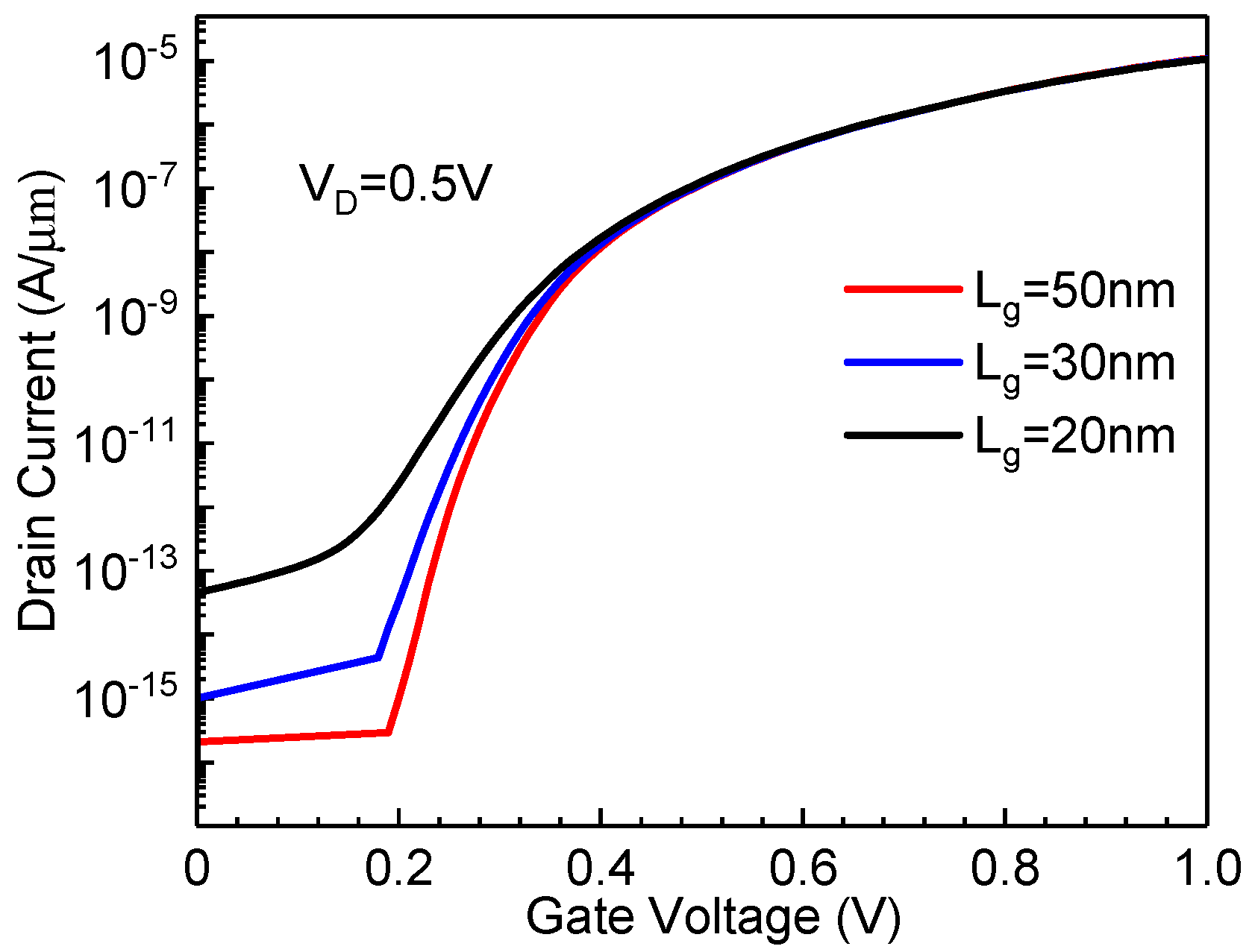
3.2. Effect of Channel Length

The long channel helps the carrier to participate in the recombination and then reduce the current in the off-state, as shown in Figure 4. In addition, once the current increases by a certain amount, the current that flows through the device depends on the BTBT generation rather than on the carrier recombination. Furthermore, increasing the size of the device facilitates heat dissipation as well as the maintenance of the high on-state current. Thus, the device channel length is set to a relatively large value (50 nm).

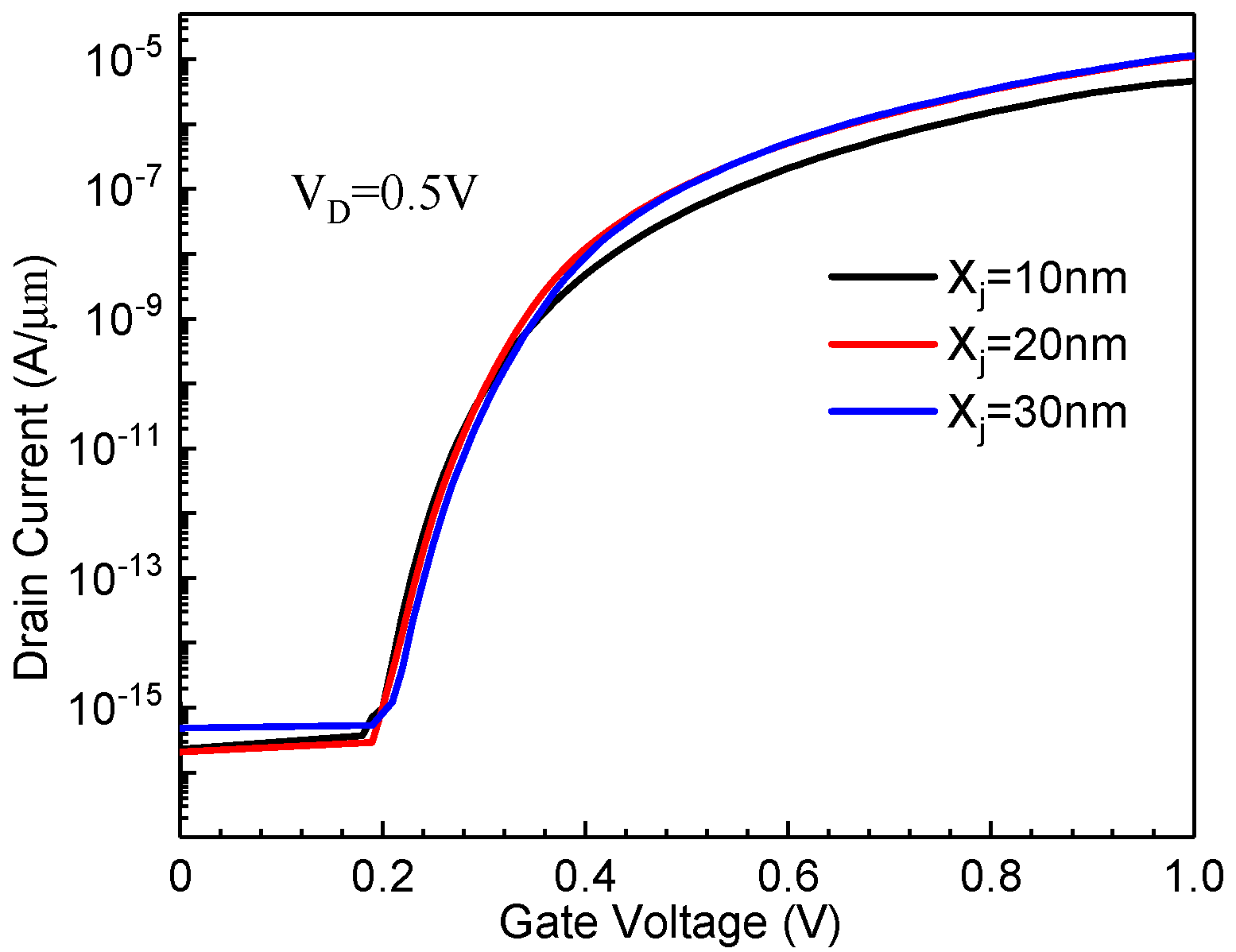
3.3. Effect of Junction Depth

It is helpful to study the junction depth of the HTFET, with respect to technology operation and device characteristics. The on-state current, as shown in Figure 5, which flows through the device, increases significantly when Xj increases from 10 to 20 nm. The junction depth increase is equivalent to increasing the tunneling area at the source-channel interface, which in turn increases the tunneling current and lowers the on-resistance. When the junction depth is set to 30 nm, the on-state current does not change significantly. This is mainly because a large number of relaxed holes accumulates at the interface between the source and the channel, which lowers the potential near the interface and degrades the band bending [14]. The default value of the junction depth in this paper was set to 20 nm.

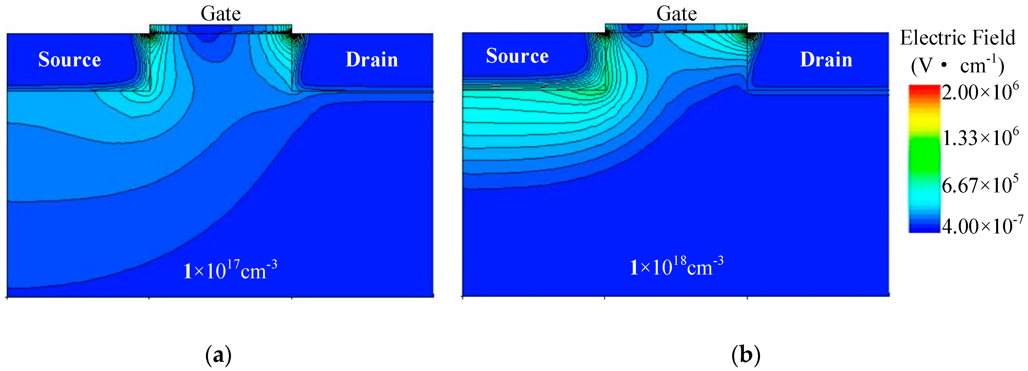
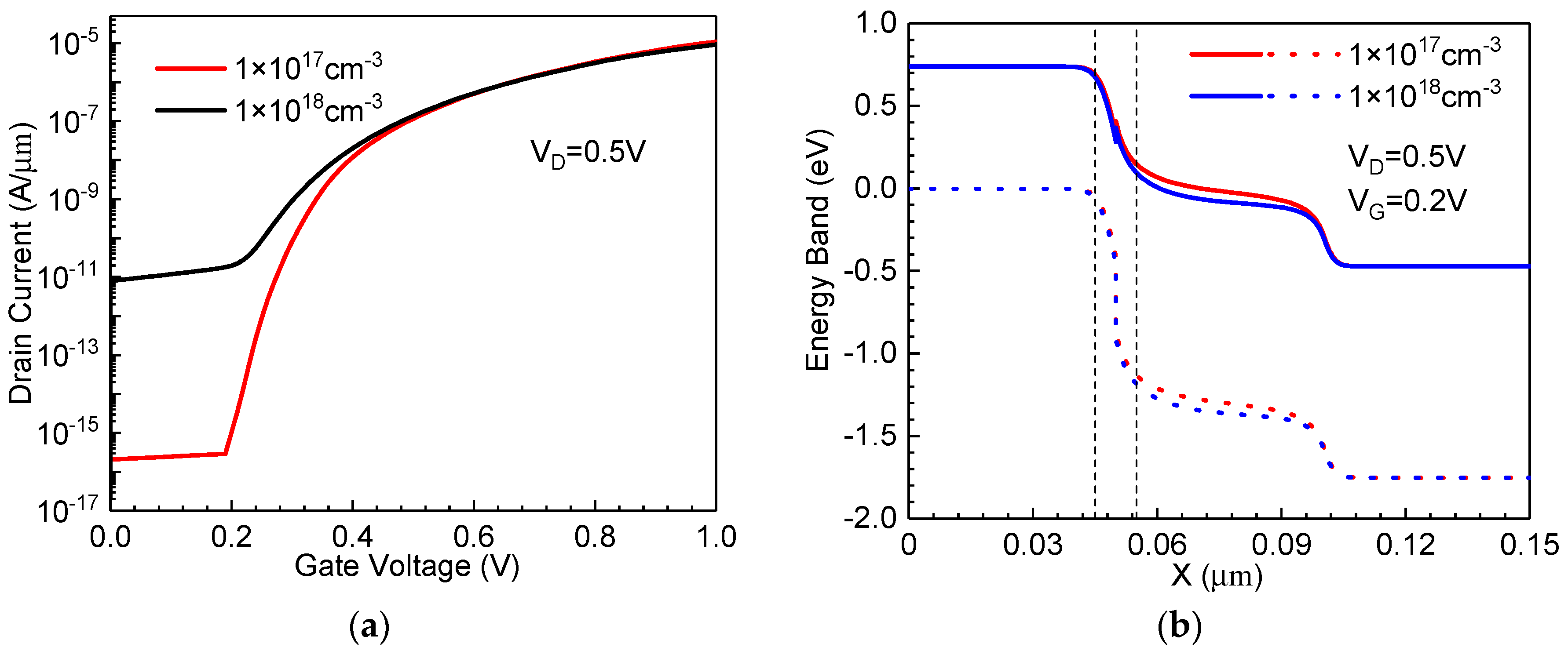
3.4. Effect of the Doping Concentration of the Substrate

Increasing the doping concentration of the substrate has undesired effects on the extension of the width of the space charge region of the PN junction and the enhancement of the electric field, as shown in Figure 6a,b. This greatly promotes the drift motion of carriers and increases the off-state current, as shown in Figure 7a. Subsequently, Figure 7b shows that when the gate bias voltage rises to 0.2 V, the substrate with a higher doping concentration will more likely lead to valence-band bending at the interface of the PN junction, which increases the BTBT current. Finally, if the VG continues to increase, the on-state current of the point-HTFETs with different substrate doping concentrations tends to saturate gradually. This is because the high voltage at the gate induces a large number of electrons underneath the gate oxide, which offset the benefits of the substrate with a high doping concentration.

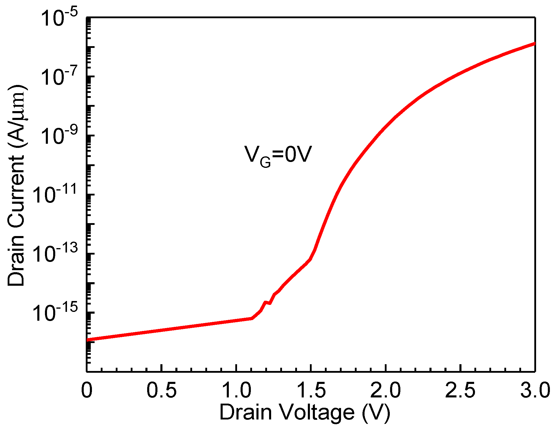
3.5. Breakdown Voltage

When the voltage between drain and substrate rises to the critical voltage (i.e., breakdown voltage), a large number of carriers, driven by the transverse electric field, begin to participate in the impact ionization and increase the drain current. As can be seen from Figure 8, the critical voltage is around 2 V, with ID = 2 nA/um.

4. The Quasi-Static Characteristics of the HTFET under TLP Stress

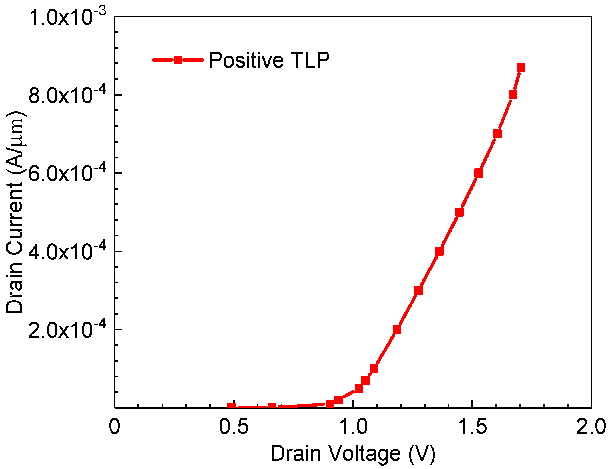
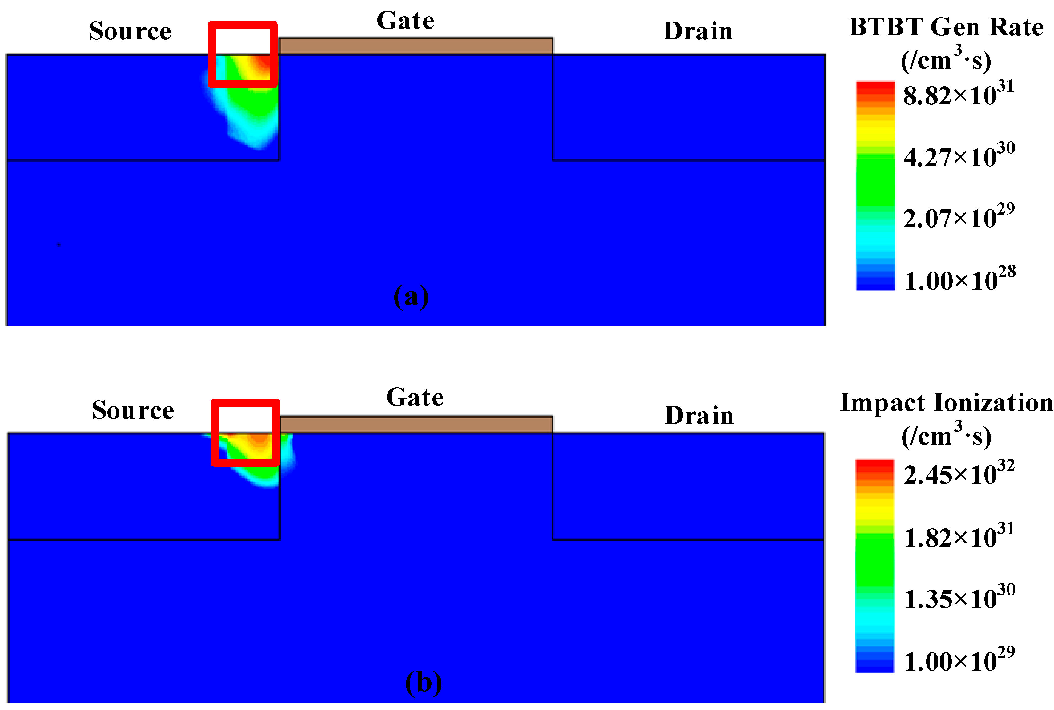
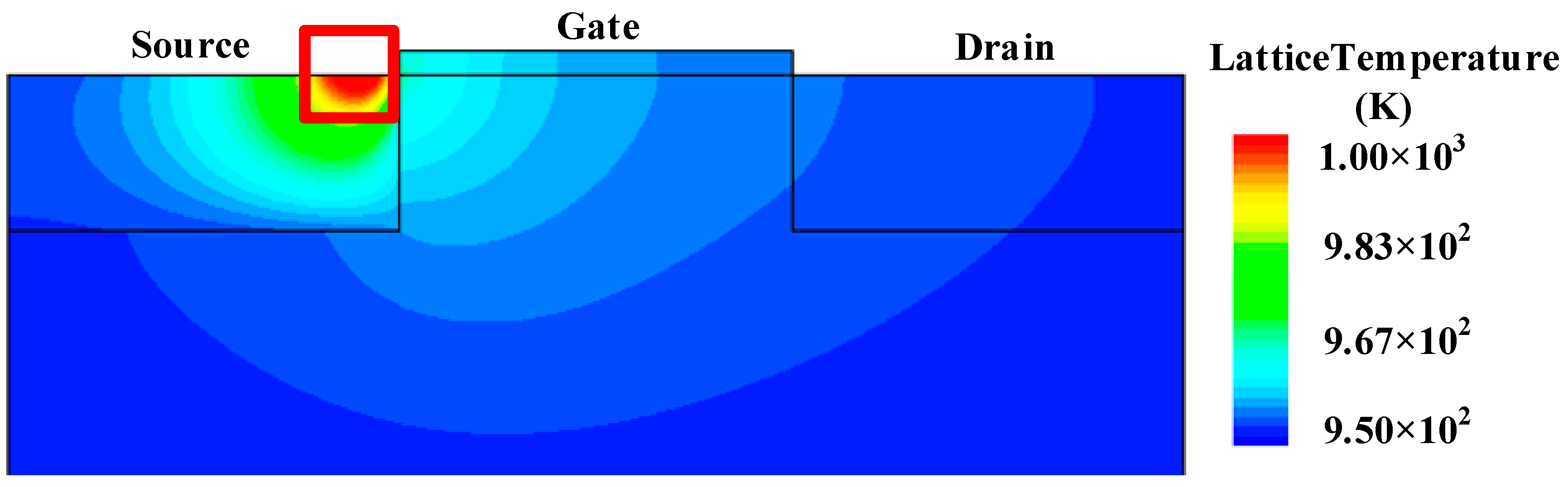
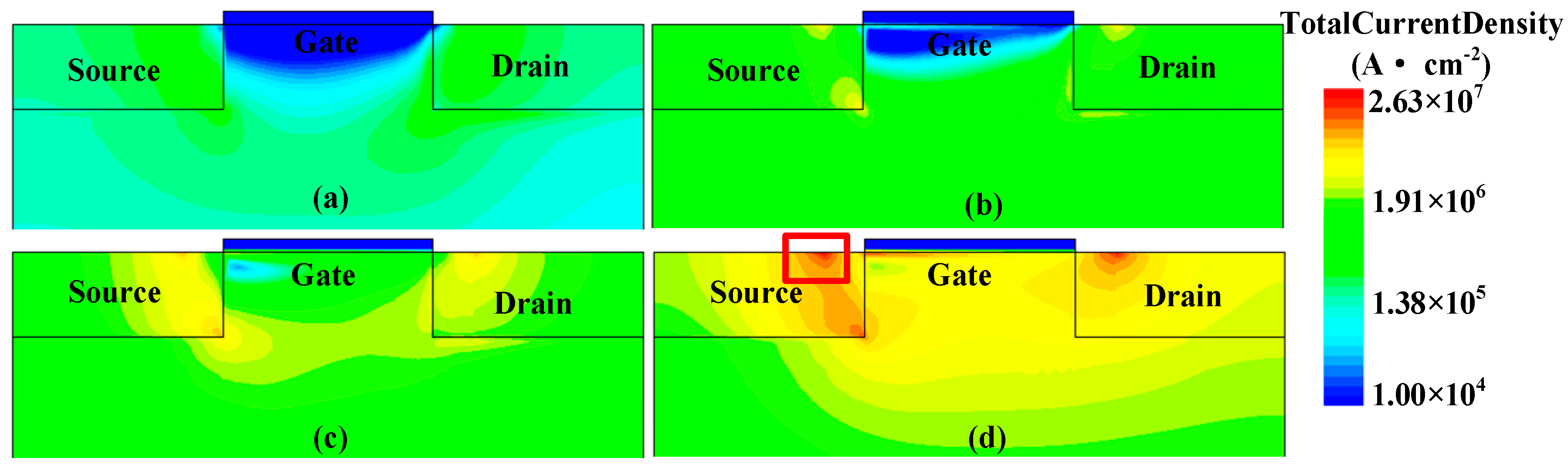
4.1. Forward Direction

In the whole-chip ESD protection network, TFETs and parasitic resistances form secondary discharge paths to assist the primary ESD discharge paths, resulting in a reduction in the clamp voltage [16]. However, the right-side boundary of the ESD window shows a decreasing trend. For example, the breakdown voltage of the thin oxide device, based on the FinFET and FDSOI, is around 2.5–3 V, which requires the clamp voltage of the ESD device to be lower than before. The HTFET is a promising candidate to help the primary ESD current path to discharge current quickly. This is because the trigger voltage and failure voltage are 1.09 and 1.71 V, respectively; see Figure 9. As a comparison, the trigger voltage and failure voltage of the silicon counterpart are around 6 and 8 V, respectively [13].
The gate of the HTFET is connected to its own drain as input, and the positive TLP current elevates the gate potential, which increases band bending between the source region and the channel. This increases the BTBT generation rate and, in turn, increases the current through the device. This BTBT current is not sufficient to turn the device on, but it acts as an initial current, which accelerates the occurrence of impact ionization. This, in turn, rapidly enhances the discharge robustness.
Figure 10a,b show the BTBT generation rate and impact ionization rate of the HTFET with a 1 × 10⁻⁴ A/um pulse, and the corresponding trigger voltage of the device is 1.09 V. As shown in Figure 11a,b, the increase in the BTBT generation rate with a large current-pulse results in an increase of the impact-ionization rate. The impact ionization of the carriers generates a large amount of heat, which will lead to the rapid increase of the lattice temperature of the HTFET. Figure 12 shows that the failure location appears on the source side. Lattice temperature, according to [19,20], is usually used as the criterion to determine device failure in simulations. The critical failure temperature is usually defined as a value that is hundreds of degrees Kelvin lower than the melting temperature. The melting temperature of materials used in this paper was selected according to [21,22].

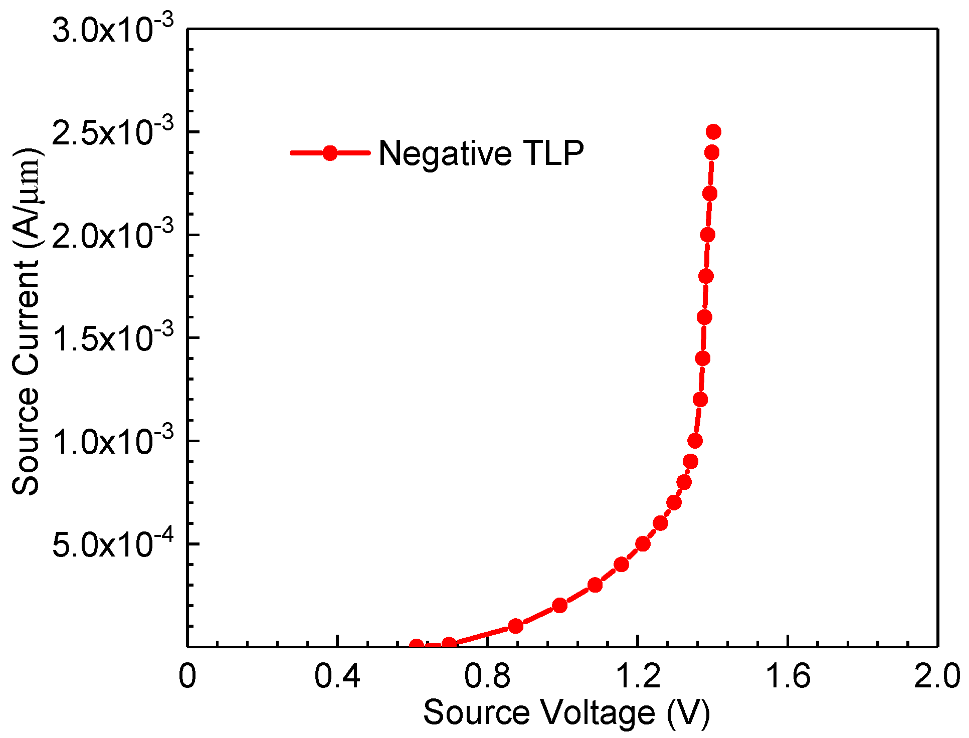
4.2. Reverse Direction

Figure 13 shows that when the source electrode serves as the current-pulse input, and the gate and drain electrodes are connected to a ground. HTFET operates like poly-bounded diodes and can conduct a high current. The device failure location, under TLP stress, is in the source region near the edge of the gate, as shown in Figure 14. In Figure 15, the current-density distribution plots for different current-pulses are (a) 1 × 10⁻⁴ A/um, (b) 5 × 10⁻⁴ A/um, (c) 1 × 10⁻³ A/um, and (d) 2.5 × 10⁻³ A/um. The high current-densities at the failure location can be clearly seen in Figure 15d. In addition, it can also be seen from Figure 16 that the electrostatic potential at the failure location is higher than in any other regions in the device. Therefore, we can conclude that occurring failures are mainly caused by high current and voltage.

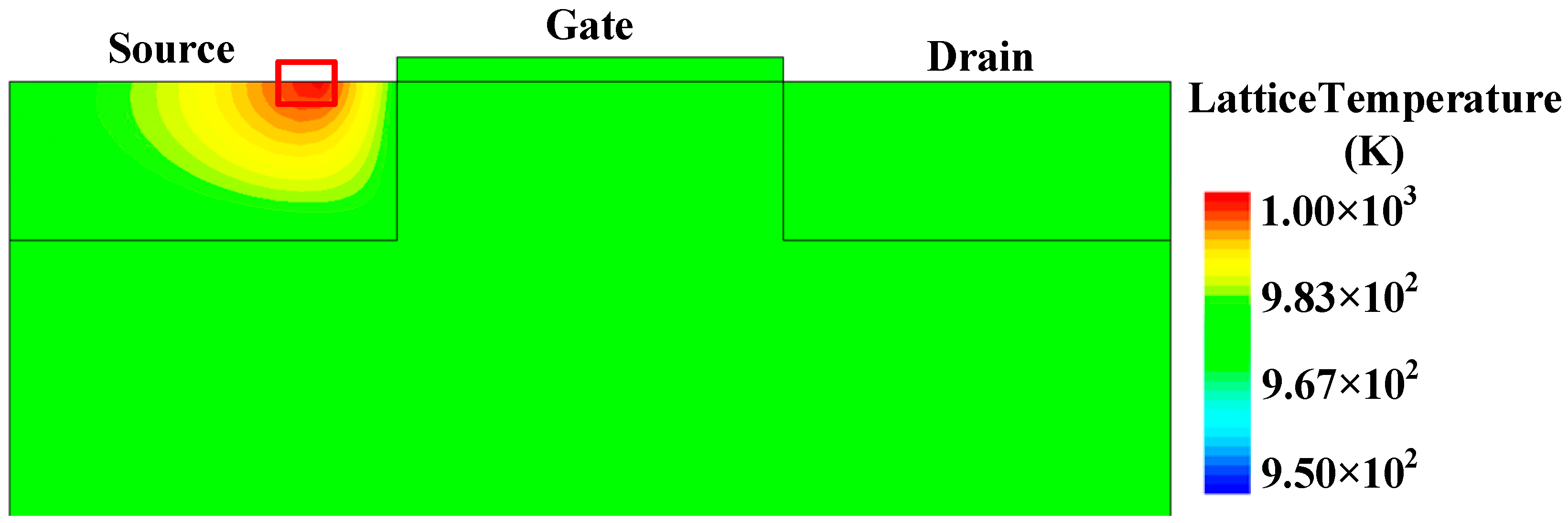
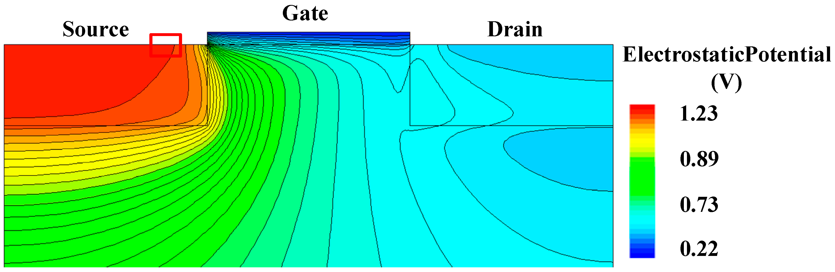
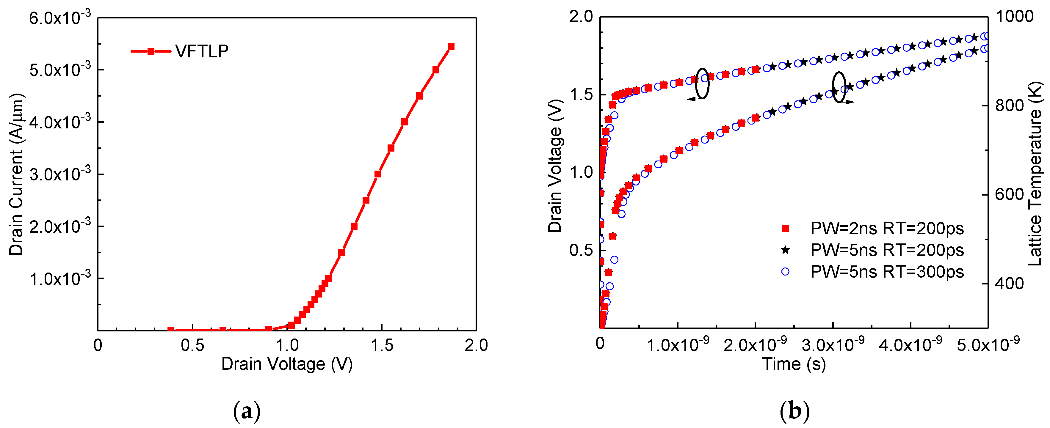
5. The Quasi-Static Characteristics of the HTFET under VFTLP Stress

Very fast transmission line pulse (VFTLP) simulation was carried out to investigate the device behavior under a charged-device model (CDM) event. Figure 17a shows the quasi-static curve, plotted by computing the average values between 1–2 ns for each positive VFTLP with a 200 ps rise time and a 2 ns pulse-width. As expected, the trend of the I–V curve was the same as for the TLP simulation. However, the failure current of the HTFET was much higher under VFTLP stress. This is mainly because an increasing pulse-width increases the lattice temperature quickly, which degrades the electrical properties. This explanation can be verified with Figure 17b, which shows the VFTLP curves with different rise times and pulse widths. It was found that pulse width has a very significant impact on the device temperature.

6. Conclusions

In this paper, the ESD characteristics of an InGaAs/InP HTFET was investigated. It was found that the InGaAs/InP HTFET has a low trigger voltage during positive TLP simulation, which makes it suitable to be used in low-voltage ICs. This became possible mainly due to the BTBT-assisted avalanche generation mechanism and its better material properties compared to its silicon counterpart. In a negative TLP simulation, the InGaAs/InP HTFET showed a similar characteristic as a poly-bounded diode. The results indicate that the InGaAs/InP HTFET can be used for the ESD protection of future III–V technology.

Author Contributions

Conceptualization, Z.Y., Z.Z.; writing—original draft preparation, Z.Z.; writing—review and editing, Z.Z., Z.Y., Y.Z., X.F., J.J.L., W.F. All authors have read and agreed to the published version of the manuscript.

Funding

This work was supported by National Natural Science Foundation of China under Grant 61804123/61874098, and in part by the Key Research and Development Program of Shaanxi Province, China under Grant 2019GY-018, and the Key Project Foundation of the Education Department of Shaanxi Province, China, under Grant 18JS082.

Conflicts of Interest

The authors declare no conflict of interest.

References

  1. Choi, W.Y.; Park, B.-G.; Lee, J.D.; Liu, T.-J.K. Tunneling Field-Effect Transistors (TFETs) With Subthreshold Swing (SS) Less Than 60 mV/dec. IEEE Electron Device Lett. 2007, 28, 743–745. [Google Scholar] [CrossRef]
  2. Ionescu, A.M.; Riel, H. Tunnel field-effect transistors as energy-efficient electronic switches. Nat. Cell Biol. 2011, 479, 329–337. [Google Scholar] [CrossRef] [PubMed]
  3. Lu, H.; Seabaugh, A. Tunnel Field-Effect Transistors: State-of-the-Art. IEEE J. Electron Devices Soc. 2014, 2, 44–49. [Google Scholar] [CrossRef]
  4. Wang, X.D.; Xiong, Y.; Tang, M.-H.; Peng, L.; Xiao, Y.G.; Xu, X.Y.; Liang, S.E.; Zhong, X.H.; He, J.H. A Si tunnel field-effect transistor model with a high switching current ratio and steep sub-threshold swing. Semicond. Sci. Technol. 2014, 29, 5–9. [Google Scholar] [CrossRef]
  5. Kim, S.H.; Agarwal, S.; Jacobson, Z.A.; Matheu, P.; Hu, C.; Liu, T.-J.K. Tunnel Field Effect Transistor With Raised Germanium Source. IEEE Electron Device Lett. 2010, 31, 1107–1109. [Google Scholar] [CrossRef]
  6. Blaeser, S.; Glass, S.; Schulte-Braucks, C.; Narimani, K.; Driesch, N.V.D.; Wirths, S.; Tiedemann, A.T.; Trellenkamp, S.; Buca, D.; Zhao, Q.-T.; et al. Novel SiGe/Si line tunneling TFET with high Ion at low Vdd and constant SS. In Proceedings of the 2015 IEEE International Electron Devices Meeting (IEDM), Washington, DC, USA, 7–9 December 2015; IEEE: New York, NY, USA, 2015. [Google Scholar]
  7. Dubey, P.K.; Kaushik, B.K. T-Shaped III-V Heterojunction Tunneling Field-Effect Transistor. IEEE Trans. Electron Devices 2017, 64, 3120–3125. [Google Scholar] [CrossRef]
  8. Zhou, G.; Lu, Y.; Li, R.; Zhang, Q.; Hwang, W.S.; Liu, Q.; Vasen, T.; Chen, C.; Zhu, H.; Kuo, J.-M.; et al. Vertical InGaAs/InP Tunnel FETs With Tunneling Normal to the Gate. IEEE Electron Device Lett. 2011, 32, 1516–1518. [Google Scholar] [CrossRef]
  9. Sant, S.; Schenk, A. Methods to Enhance the Performance of InGaAs/InP Heterojunction Tunnel FETs. IEEE Trans. Electron Devices 2015, 63, 2169–2175. [Google Scholar] [CrossRef]
  10. Dong, A.; Xiong, J.; Mitra, S.; Liang, W.; Gauthier, R.; Loiseau, A. Comprehensive Study of ESD Design Window Scaling Down to 7nm Technology Node. In Proceedings of the 2018 40th Electrical Overstress/Electrostatic Discharge Symposium (EOS/ESD), Reno, NV, USA, 23–28 September 2018; Institute of Electrical and Electronics Engineers (IEEE): New York, NY, USA. [Google Scholar]
  11. Mergens, M.P.J.; Russ, C.C.; Verhaege, K.; Armer, J.; Jozwiak, P.C.; Mohn, R.P.; Keppens, B.; Trinh, C.S. Speed optimized diode-triggered SCR (DTSCR) for RF ESD protection of ultra-sensitive IC nodes in advanced technologies. IEEE Trans. Device Mater. Reliab. 2005, 5, 532–542. [Google Scholar] [CrossRef]
  12. Galy, P. Electro Static Discharge (ESD) one real life event: Physical impact and protection challenges in advanced CMOS technologies. In Proceedings of the 2014 International Semiconductor Conference (CAS), Sinaia, Romania, 13–15 October 2014; Institute of Electrical and Electronics Engineers (IEEE): New York, NY, USA; pp. 31–34. [Google Scholar]
  13. Galy, P.; Athanasiou, S. Preliminary results on TFET—Gated diode in thin silicon film for IO design & ESD protection in 28nm UTBB FD-SOI CMOS technology. In Proceedings of the 2016 International Conference on IC Design and Technology (ICICDT), Ho Chi Minh City, Vietnam, 27–29 June 2016; Institute of Electrical and Electronics Engineers (IEEE): New York, NY, USA; pp. 1–4. [Google Scholar]
  14. Kranthi, N.K.; Shrivastava, M. ESD Behavior of Tunnel FET Devices. IEEE Trans. Electron Devices 2016, 64, 28–36. [Google Scholar] [CrossRef]
  15. Yang, Z.; Zhang, Y.; Yang, Y.; Yu, N. Investigation of the Double Current Path Phenomenon in Gate-Grounded Tunnel FET. IEEE Electron Device Lett. 2017, 39, 103–106. [Google Scholar] [CrossRef]
  16. Sithanandam, R.; Kumar, M.J. A New On-Chip ESD Strategy Using TFETs-TCAD Based Device and Network Simulations. IEEE J. Electron Devices Soc. 2018, 6, 298–308. [Google Scholar] [CrossRef]
  17. Colinge, J.-P.; Alderman, J.C.; Xiong, W.; Cleavelin, C.R. Quantum-mechanical effects in trigate SOI MOSFETs. IEEE Trans. Electron Devices 2006, 53, 1131–1136. [Google Scholar] [CrossRef]
  18. Sahay, S.; Kumar, M.J. Insight into Lateral Band-to-Band-Tunneling in Nanowire Junctionless FETs. IEEE Trans. Electron Devices 2016, 63, 4138–4142. [Google Scholar] [CrossRef]
  19. Wang Albert, Z.H. On-chip ESD Protection for Integrated Circuits: An IC Design Perspective; Springer US: Manhattan, NY, USA, 2002; p. 233. [Google Scholar]
  20. Yang, Z.; Yang, Y.; Yu, N.; Liou, J.J. Improving ESD Protection Robustness Using SiGe Source/Drain Regions in Tunnel FET. Micromachines 2018, 9, 657. [Google Scholar] [CrossRef] [PubMed] [Green Version]
  21. Brenchley, M.E.; Hopkinson, M.; Kelly, A.; Kidd, P.; Dunstan, D.J. Coherency Strain as an Athermal Strengthening Mechanism. Phys. Rev. Lett. 1997, 78, 3912–3914. [Google Scholar] [CrossRef]
  22. Lim, C.G. Thermal Modeling of Intersubband Transition-Based InGaAs/AlAsSb Ultrafast All-Optical Cross-Phase Modulators. IEEE J. Quantum Electron. 2010, 46, 610–617. [Google Scholar] [CrossRef]
Figure 1. Tunneling parameters calibrated according to [9].
Crystals 10 01059 g001
Figure 2. Schematic of the HTFET (heterojunction tunneling field effect, not to scale).
Crystals 10 01059 g002
Figure 3. (a) Transfer curves of the HTFET with different doping concentrations in the source region. (b) Band diagram of the HTFET in the on-state.
Crystals 10 01059 g003
Figure 4. Transfer curves of the HTFET for different channel lengths.
Crystals 10 01059 g004
Figure 5. Transfer curves of the HTFET for different junction depths.
Crystals 10 01059 g005
Figure 6. Contour plots of the electric field at the interface between source and substrate with doping concentrations of (a) 1 × 1017 cm−3 and (b) 1 × 1018 cm−3.
Crystals 10 01059 g006
Figure 7. (a) Transfer curves for the HTFET with different doping concentrations of the substrate. (b) Band diagram of the HTFET for different doping concentrations under the same bias voltage.
Crystals 10 01059 g007
Figure 8. The output characteristic of the HTFET.
Crystals 10 01059 g008
Figure 9. Simulated transmission line pulse (TLP) curves in the forward direction of the HTFET.
Crystals 10 01059 g009
Figure 10. (a) BTBT (band-to-band tunneling) generation rates for the HTFET with a 1 × 10⁻⁴ A/um pulse; (b) impact ionization rates for the HTFET with a 1 × 10⁻⁴ A/um pulse.
Crystals 10 01059 g010
Figure 11. (a) BTBT generation rates for the HTFET with a 8.7 × 10⁻⁴ A/um pulse; (b) impact ionization rates for the HTFET with a 8.7 × 10⁻⁴ A/um pulse.
Crystals 10 01059 g011
Figure 12. Temperature-distribution map at the last moment.
Crystals 10 01059 g012
Figure 13. Simulated TLP curves in the reverse direction of the HTFET.
Crystals 10 01059 g013
Figure 14. Temperature distribution map at the last moment.
Crystals 10 01059 g014
Figure 15. Current density distribution maps for (a) 1 × 10⁻⁴ A/um, (b) 5 × 10⁻⁴ A/um, (c) 1 × 10⁻³ A/um, and (d) 2.5 × 10⁻³ A/um pulses.
Crystals 10 01059 g015
Figure 16. Equipotential distribution map at the last moment.
Crystals 10 01059 g016
Figure 17. (a) Simulated very fast transmission line pulse (VFTLP) curves in the positive direction for the HTFET; (b) VFTLP properties of the HTFET for pulse durations of 2 ns (RT = 200 ps) and 5 ns (RT = 200 ps and 300 ps).
Crystals 10 01059 g017
Table 1. Parameters calibrated for nonlocal band-to-band tunneling model.
ParameterUnitIn0.53Ga0.47AsInP
EgeV0.741.35
Electron affinityeV4.54.38
mtem00.0430.08
mthm00.0520.12
Degeneracy122
Publisher’s Note: MDPI stays neutral with regard to jurisdictional claims in published maps and institutional affiliations.

