Designing Metasurfaces with Canonical Unit Cells


1
Ericsson Nikola Tesla d.d., Research and Development Center, Krapinska 45, 10002 Zagreb, Croatia
2
Faculty of Electrical Engineering and Computing, University of Zagreb, Unska 3, 10000 Zagreb, Croatia
*
Author to whom correspondence should be addressed.
Crystals 2020, 10(10), 938; https://doi.org/10.3390/cryst10100938
Submission received: 31 August 2020
/
Revised: 7 October 2020
/
Accepted: 13 October 2020
/
Published: 15 October 2020
(This article belongs to the Special Issue Polarization-Handling Metasurfaces)
Abstract
:Among different approaches to designing metasurfaces, surface sheet impedance is proving to be a straightforward path for many applications. Recent publications have proposed several methods for optimizing this design approach, enabling rapid metasurface development. Upon finding the requirements using the sheet impedance approach, design continues with the selection of unit cell geometry. This choice is usually based on approximate expressions that have been published throughout the years. We review the approximate expressions for metasurface unit cell design, with consideration of their applicability to certain applications, namely polarization-dependent beam-shaping metasurfaces. We evaluate the accuracy of the approximate expressions against simulation results from a full-wave electromagnetic solver, and propose an optimization approach to correct the proposed design for the observed error. The applicability of different unit cell types is discussed, especially considering the limitations of technological processes typically used in metasurface production. A prototype was developed to verify the validity of this design approach.
1. Introduction
The design of modern antennas, and electromagnetic (EM) systems in general, focuses on tailoring the EM field at the emitting aperture. Tailoring can comprise of defining the beam shape, beam pointing direction, and beam polarization. Metasurfaces (MTS) are thin two-dimensional metamaterial layers that have the capability of manipulating EM waves. They can be used to allow or inhibit the propagation of EM waves in the desired directions, or confine the waves to avoid undesired leakage of energy so as to increase the overall efficiency of electromagnetic devices [1]. Because of their low profile and properties such as low loss, metasurfaces have recently been successfully applied in numerous applications such as antenna design [2], polarizers and polarization converters [3,4], for wavefront manipulation and in controlling guided modes [5,6,7].
A metasurface layer can be characterized by surface boundary conditions, referred to as Generalized Sheet Transition Conditions (GSTC) [8,9]. These are based on a physical model of metasurface cells as polarizable particles. Electric, magnetic and magnetoelectric responses are described by a corresponding equation that relates the average tangential EM field at the metasurface to the currents along it. Synthesis of metasurfaces can start with the GSTC and determining the spatial distribution of corresponding electric sheet admittance, magnetic sheet impedance and magnetoelectric response. Alternatively, we could start with a typical practical implementation consisting of a cascade of metasurfaces that exhibit electric response only, separated by subwavelength dielectric spacers [4]. In this way, a metasurface structure with a wide range of functionalities can be obtained, such as polarization manipulation, beam focusing, beam tilting, increased bandwidth and angular performance. (See, e.g., [3,4,10].) The number of design parameters embedded in each metasurface unit cell design directly determines the number of degrees of freedom in the design, and ultimately the required number of layers for the cascaded structure.
The design of metasurface structures is then based on determining the spatial distribution of the sheet impedance tensor for each metasurface layer in the cascade. However, the knowledge of the desired value of the sheet impedance tensor does not uniquely determine the shape of the metallic pattern. Note that the metasurface bandwidth is generally larger for implementations based on simple canonical metallic shapes [11]. The aim of this paper is to discuss the properties of different canonical metallic patterns and the range of values of sheet impedances that each can achieve.
This paper is organized as follows: In Section 2 we introduce canonical and some more complex unit cell designs. We review the approximate expressions for finding the surface sheet impedance of these unit cells from their design parameters. In Section 3 we compare the performance as analyzed using the approximate expressions with the results obtained using a full-wave EM simulator. In Section 4 we discuss the observed results and propose a procedure for finding the optimal unit cell design parameters with the approximate expressions as a starting point. We evaluate the performance of the entire procedure by comparing the simulation and measurement results of a developed prototype metasurface in Section 5. Finally, the paper is concluded with Section 6 where we review the presented contributions.
2. Approximate Expressions
To unify the approach at which we analyze these structures, we will take an exemplary planar metasurface, constructed as an infinite 2D array of unit cells with a general setup depicted in Figure 1. The discrete unit cells are the prime focus of this paper. We place them at a period P in both planar (x and y) dimensions. In this paper, period P is assumed to be subwavelength, i.e., . Boundary conditions at each cell period P are periodic, while in the z direction, open space conditions are assumed. We will analyze the MTS through its sheet impedance, with the MTS having electric response only, as discussed in the previous section. The boundary condition can be stated as follows:
Here, denotes the average electric field at the MTS layer, and are the magnetic field at the outer and inner MTS boundaries respectively, the average surface current, the sheet impedance tensor, and the outward-pointing unit vector normal to the metasurface layer.
The structures we are about to review will have their principal design characteristics aligned with either the x or the y axis, as seen in Figure 1. Mostly, these structures will have symmetry that allows us to exchange the presented analysis between the x- and the y-polarization. Throughout this analysis, we refer to parallel elements as those parallel to the y axis, and perpendicular elements as those parallel to the x axis. In a general case, the plane wave will be incident to the plane of the MTS under the angle relative to the z axis. TE incidence denotes an incident wave that has its field parallel to the y axis. In the case of TM incidence, field is parallel to the y axis.
The approximate expressions for unit cell sheet impedances are either obtained through analytical analysis of an equivalent transmission-line model representing the unit cell, or, more seldom, through rigorous numerical analysis, which results in empirical functions and constants. In each case, the expressions take the interaction between adjacent unit cells into account. For example, two adjacent loop unit cells form a capacitive interaction, which is the basis for the analytical expression. From the information on sheet impedance, we will be able to analyze other EM parameters, such as S-parameters.
The simplest form of a unit cell is a strip spanning across the entire period in one direction. A strip can exhibit either high inductivity or high capacitance at lower frequencies, depending on the direction it is placed along with respect to the polarization vector. It is illustrated in Figure 2. For an angle of incidence , sheet impedances of capacitive perpendicular strips for TE and TM incidences are given as [12,13,14]
Here, is the intrinsic impedance of free-space, and is the relative permittivity of a homogenized substrate found by analyzing the substrate on both sides of the unit cell. Considering bulk substrates on both sides, we find the homogenized substrate’s effective relative permittivity simply as
An inductive, parallel strip has a sheet impedance of
An extension of this type of unit cell is the grid mesh. The difference in analytical expressions between parallel strips and a grid mesh is in the 0.5 factor in the coefficient related to wave incidence angle of a TM-polarized wave [13]:
A complementary structure of grid mesh is a patch array, shown in Figure 3a. This can be analyzed using Babinet’s principle against the grid mesh [15], employing:
and analogously for the other pair of wave incidences. As the unit cell has a gap between metallic patterns, capacitive behavior is expected due to the presence of the component of the electric field perpendicular to conductive elements.
Similar behavior could be expected for loops, which are presented in Figure 3b. This particular unit cell features at least two free design variables. (One more if we do not preserve the 1:1 rectangle side ratio, etc.) For this unit cell, sheet impedance is the same for both polarizations, and amounts to [16]
Note that a grid mesh unit cell can be obtained from a loop by setting .
Another modification of strips is a very versatile meander line unit cell. It is very effective in handling both polarizations, and has a large number of design parameters, only some of which are presented in Figure 4. In its basic form, it consists of parallel strips that are displaced by a period of . The displacement is performed by introduction of sections of perpendicular strips, h in length starting from the inner side of one perpendicular strip to the edge of the structure. To emphasize the large number of free design variables supported by the approximate expression, we annotated the previously used unit cell period P as (the alluding to the orientation of strips along the x axis), and introduced as the period of strips along the y axis.
Meander lines have been thoroughly modeled in [17] by mapping their constituent geometrical elements into equivalent electrical impedances and admittances. Partially empirical expressions have been proposed. Here, we present the expression for a TE-incident wave:
where f is the frequency in GHz, and . For incidence perpendicular to the meander line, readers are encouraged to look into [17]. The option to arbitrarily choose the displacement between two perpendicular strips is out of the scope of this expression.
3. Comparison To Simulations
We will now compare how the presented approximate expressions perform against the results obtained by simulation in a full-wave EM solver. For each of the designs, we can take one free design variable at a time. With strips, strip width w is the only one we can use, while for a structure such as meanders, we can define at least three free design variables. For such designs, we have chosen a few design variables that we consider to give representative results for understanding the variance of electrical parameters with different designs. For some cell designs we observed the behavior when sweeping multiple variables. The design parameter that is being swept will then be denoted as .
By analyzing a given unit cell as a single, periodic layer of a metasurface, we can convert the sheet impedance of the MTS to its S-parameters. This is done by analyzing the thin layer in a transmission-line equivalent circuit [3]. For a normally-incident wave, we present the equivalent circuit in Figure 5.
To be able to find the phase shifts achievable by the unit cells, we calculate S-parameters for a normally-incident wave as
For an obliquely incident wave, the modification of the equivalent circuit and Equation (12) is straightforward, as the characteristic impedance of free-space needs only be modified by a cosine factor of the incidence angle as [13]
Unit cells were modeled in computer-aided design (CAD) software and analyzed in a full-wave EM solver to verify the results of this analysis. For that purpose we used CST Microwave Studio [18]. Unit cell performance is simulated with periodic boundary conditions in x and y directions; The structure is considered to be an infinite 2D array made up of the considered unit cell, as was the case with the approximate expressions. The structure is excited by a plane wave or, in the case of a frequency-domain solver, by the basic Floquet mode of a port defined at the end of the z domain of the unit cell, which has an open boundary. We measure the transmission coefficient between and coordinates of the simulation space, keeping a note of the free-space propagation phase offset. The incident wave is y-polarized and normally-incident to the modeled MTS. The observed can now be compared to that found by the analysis. Sheet impedance of the simulated structure can also be found by inverting Equation (12) for .
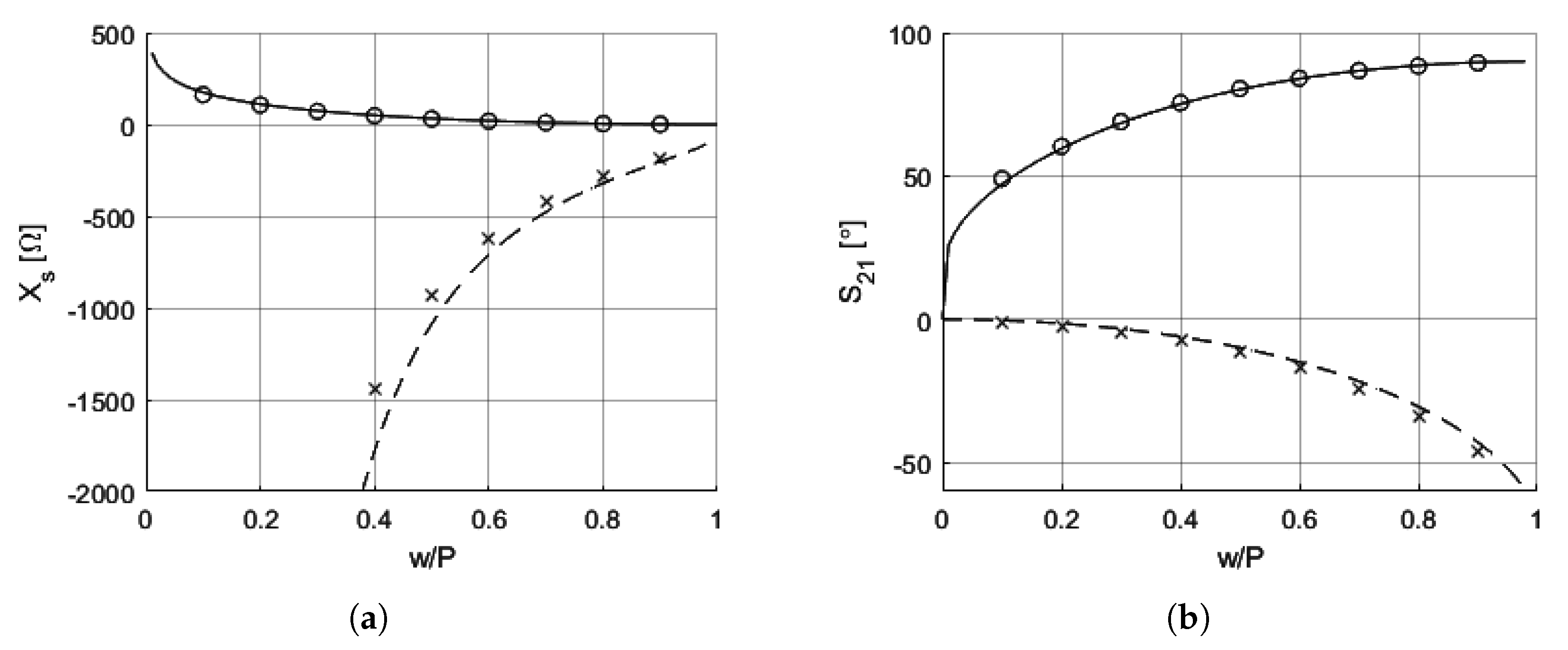
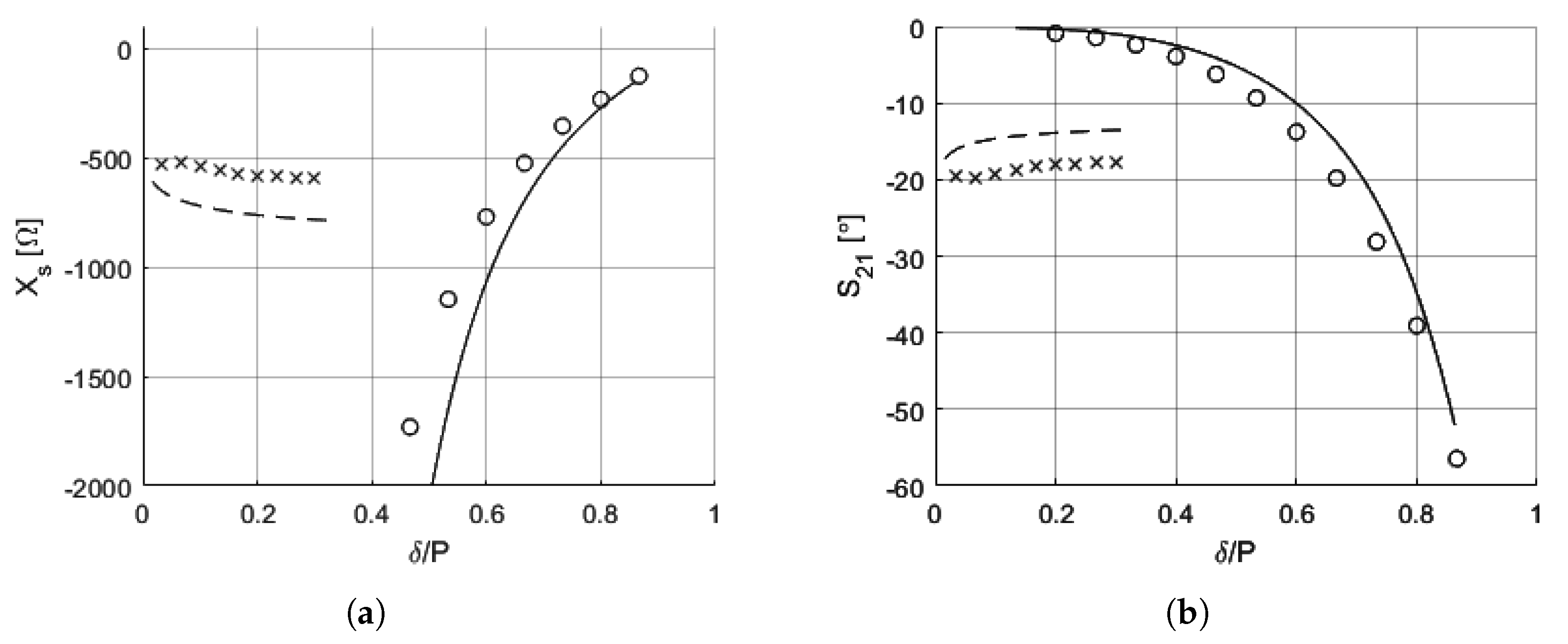
The unit cells are modeled with a period and analyzed at a frequency of 10 GHz. These parameters were chosen as they will best fit the prototype metasurface, which will be presented in Section 5. The results for each unit cell design are shown in Figure 6, Figure 7, Figure 8 and Figure 9.
It is only for parallel strips that we have perfect matching between analysis and simulation results. For all other unit cell designs, we can confirm that the previously published approximate expressions are correct in presenting the shape of the function that the unit cells’ electrical characteristics follow. However, surface reactance values need additional tuning using an accurate general EM solver. Still, the approximate dimensions of the metallic patterns can be determined using the approximate expressions.
Having presented variable sweeps with a fixed unit cell period, we now look into how surface impedance changes with varying unit cell period. It should be noted that the ratio is present in all expressions. Therefore, in presenting the numerical results, we normalized the obtained surface impedance with a normalization factor for predominantly inductive unit cell designs, and with for predominantly capacitive designs. The comparison of normalized surface impedances obtained by an analytical approach and simulations is presented in Figure 10.
From the results presented in Figure 10a,b, several conclusions can be drawn. First, the accuracy of the approximate expressions for surface impedance is only weakly dependent on the cell period. Second, with increasing period the expressions are sufficiently precise, and will remain so until the emergence of higher-order modes. It should be noted that for loops none of the above conclusions seem to hold when observing Figure 10c. This, however, is expected, as loops consist of both inductive and capacitive elements. In this analysis, the normalization factor was taken as , due to the fact that capacitive elements are dominant in defining the behavior of loops. The presence of inductive elements introduce a non-constant profile in Figure 10c due to inadequate normalization. The same is expected to happen with meander lines, although their analysis was omitted here due to higher complexity of the design.
When designing metasurfaces based on their sheet impedance, the error introduced by the approximate expressions can be significant with some of the cell designs. To counteract the error, a simple optimization procedure can be applied, such as a gradient-based quasi-Newton method, with the results from the approximate expressions as a starting point. Such optimization routines are part of most commercial EM solvers. The goal requirement for the optimization procedure is to bring the sheet impedance (and subsequently, phase shift) of a given unit cell as close to the original requirement as possible. The other option is to create a look-up table using a general EM solver, which maps sheet impedances to metallic pattern dimensions. Such a look-up table would cover the range of parameters of interest. For unit cell designs that provide multiple free design variables, this procedure could be simplified, as a more educated guess for the starting point of the optimization procedure can be made. This is possible after examining the impact any of the design variables have on sheet impedance (and subsequently phase shifts), by, for example, inspecting the calculated look-up table. The extra design variables are then better defined and fixed before proceeding with the optimization procedure. In practice, we found that the optimization procedure results in small changes to one or two design variables to achieve the desired electrical characteristics.
4. Selection of Unit Cells
4.1. Relevant Design Parameters
Having presented a number of unit cell types in the previous sections, we can compare their performance by a number of factors, depending on the metasurface requirement. When talking about beam-shaping and polarization-handling metasurfaces, the prime requirement on unit cell design is the phase shift. For all the presented designs, we have been observing a single-variable design sweep, although all considerations stand if we wish to do a more advanced design approach with multiple free variables.
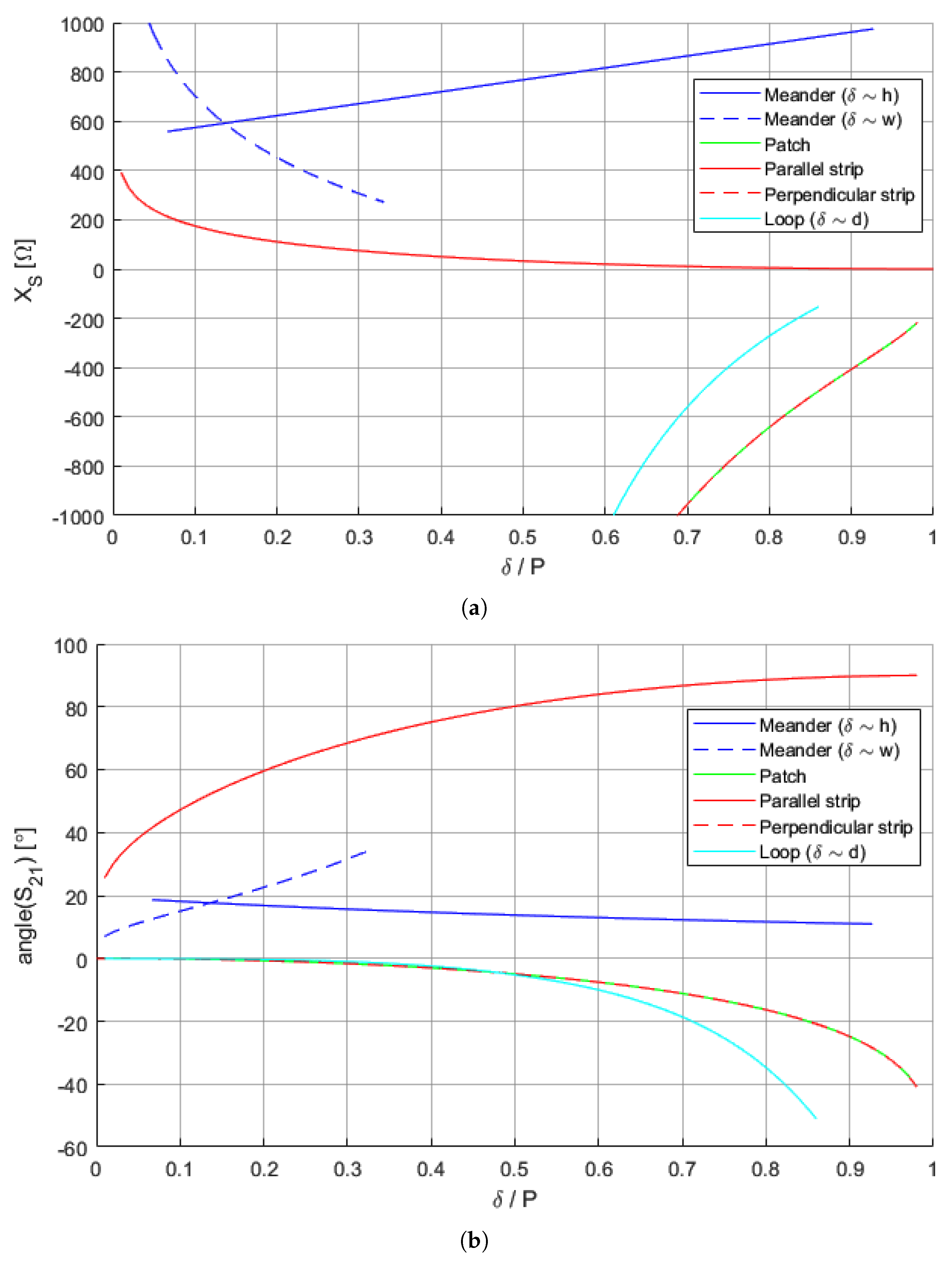
To put all the presented unit cell designs in perspective, we can estimate the ranges of sheet reactances and phase shifts achievable by these designs. This is presented in Figure 11. Using only a handful of unit cell designs, a large range of electrical parameters can be reached when sweeping some of their design parameters. Depending on the MTS function we wish to accomplish, the profile of the required sheet impedance may restrict design capabilities. It should be noted, however, that any phase profile can be wrapped around so that the initial unit cell phase can be freely selected. This should facilitate the design for many applications, as at least of the phase shift domain can be easily reached. Figure 11 can thus serve as an engineering guideline when selecting the unit cell design. Care should be taken to choose the unit cell design that will keep the structure’s surface impedance high (i.e., higher than free-space impedance surrounding the MTS), as such selection will minimize the reflection coefficient, as seen in Equation (12). If, however, we cannot avoid small impedance values, multi-layer MTS design should be favored.
4.2. Development Restrictions
When developing an MTS of this kind, certain caveats have to be kept in mind due to the restrictions posed by the development technology. Recently, research on curved metasurfaces had covered the manufacturing process to some extent [19]. The production of planar and simply-curved MTS layers has been suggested by exploiting the common printed circuit board (PCB) manufacturing techniques. These could either be based on chemical processes, such as etching, preceded by either a photolithographic or other type of mask transfer, or it could be a mechanically-subtractive process, such as layer milling using specialized machines.
Any of these techniques produce an MTS with certain imperfections, namely due to different precision and tolerances in producing the required geometric shape. Observing Figure 11a, we find a highly dynamic reactance profile, i.e., a high , for some designs. A less precise development technique will lead to uncertainty in the actual achieved sheet reactance. If a unit cell is considered in a purely periodic environment, this may not lead to greater issues, if the corresponding phase shift profile of the unit cell in question is relatively stable. However, when found in a non-homogeneous environment, with multiple different unit cells in the area, and especially when found in a finite structure, the unexpected value of sheet reactance will change the macroscopic relations between unit cells in an unwanted way, leading to incorrect phase shifts in all.
This leads us to another caveat. While we are able to cover a large span of sheet reactances using only a handful of unit cell types and design variables, we encounter problems when exploiting this ability to a greater extent. An MTS comprised of different unit cells will exhibit unexpected phase shifts when adjacent unit cells’ sheet reactances are too far apart. While we do not consider this phenomenon in detail in this paper, we found that the best way to select unit cells in non-homogeneous environments is to keep a relatively small deviation of the sheet impedance between adjacent unit cells.
For all these reasons, we favored the use of simple and versatile unit cell types in all our experimental metasurface designs. Specifically, we found strips and meander lines to be a reliable choice for beam-shaping MTSs. In Section 5 we will closely look into a representative MTS prototype.
4.3. Multi-Layer Metasurfaces
Reconsidering Equation (12), it can be seen that an arbitrary MTS function cannot be achieved using a single-layer metasurface whilst preserving a high transmission coefficient. This can be overcome by using multi-layer metasurfaces. As it is shown in [4], the design of metasurfaces that exhibit arbitrarily chosen transmission properties can be performed in two steps. First, we map the transmission and reflection parameters, i.e., the S-parameter matrix, to the parameters of a single-layer bianisotropic metasurface: electric sheet admittance tensor, magnetic sheet impedance tensor, and dimensionless magnetoelectric coupling tensors. The S-parameter matrix will by design define the response to both orthogonal polarizations. Furthermore, we also obtain a physical understanding of the desired MTS structure. Next, we investigate the implementation of the desired bianisotropic metasurface using a cascade of anisotropic, patterned metallic sheets, where each individual sheet is described only by its electric sheet admittance tensor. One needs at least three cascaded metallic sheets to implement a general bianisotropic metasurface. Four sheets are often used to allow for added bandwidth, while for some applications fewer layers can suffice.
This approach has proven successful for designing metasurfaces for controlling polarization, wavefront and beam shape [3,10]. For example, a polarization rotator has a strong chiral response, so the needed bianisotropic response can be obtained with an isotropic and chiral metasurface. A four-layer cascaded realization is described in [4]. A symmetrical circular polarizer is traditionally obtained using a quarter-wave plate and a linear polarizer, which results in a bulky structure. In metasurface implementation a bianisotropic metasurface exhibits anisotropic electric and magnetic susceptibility, as well as magnetoelectric coupling. However, in some cases it is simpler to proceed directly with designing a cascaded metasurface structure using the desired S-parameters. Note that a single bianisotropic boundary is a fictitious local boundary condition where the normally-incident power must be conserved not just globally, but also locally for a lossless metasurface [9].
The unit cell design approach presented in this paper can easily be applied without the use of global optimization procedures suggested by previous works.
5. Prototype And Measurements
In our recent research, we presented several methods for obtaining an MTS sheet impedance profile from a functional requirement [19,20,21,22]. Focus was placed on beam-steering metasurfaces, notably curved structures. While the prime focus of these papers was to present an analysis method for obtaining the required sheet impedance profile, here we discuss the design methodology and its application on the development of the MTS structure proposed in [19].
A curved metasurface, semi-cylindrical in shape, is proposed. It shall consist of one layer, 12 cm in diameter. No additional conductive layers shall be used. The supporting substrate material with and thickness of shall be used, and it will be considered when designing the metasurface. The structure is intended to shape the radiation pattern of an omnidirectional source placed at the center of the cylinder. We would like to achieve two beams at angles, i.e., two beams symmetrically against the center of the structure. The operating frequency is 10 GHz.
The structure itself is symmetric, consisting of four bent plates, each spanning one-eighth of the cylinder, and each with six different types of unit cells placed along the axis. The metasurface is homogeneous along the y axis. The cell period is taken as 7.854 mm to produce a semi-cylinder of the given radius. The sheet impedance profile of such a metasurface achieving the desired function was found by utilizing one of the methods presented in earlier works [19,20,21,22]. We then examine Figure 11a and determine the appropriate type of each unit cell. Using the approximate expressions discussed in Section 2, we find the initial design parameters, which are presented in Table 1. We then apply the optimization procedure proposed in Section 3 to obtain the final design. The approximate expressions produced sufficiently precise results for strip type of unit cells. Any further optimization would not yield better results, as the difference between the initial and the optimized design would become too fine for the manufacturing process to deliver. Therefore, only meander line design parameters have been changed, as presented in Table 1.
The MTS was first modeled in CAD and simulated in CST Microwave Studio. Its response on both x- and y-polarization was observed, with a short dipole set as the source. The results presented in Figure 12 represent the expected response of the produced MTS. It shapes the omnidirectional pattern of an y-oriented dipole into the desired pattern, whilst not disturbing the cosine radiation pattern of an x-oriented dipole.
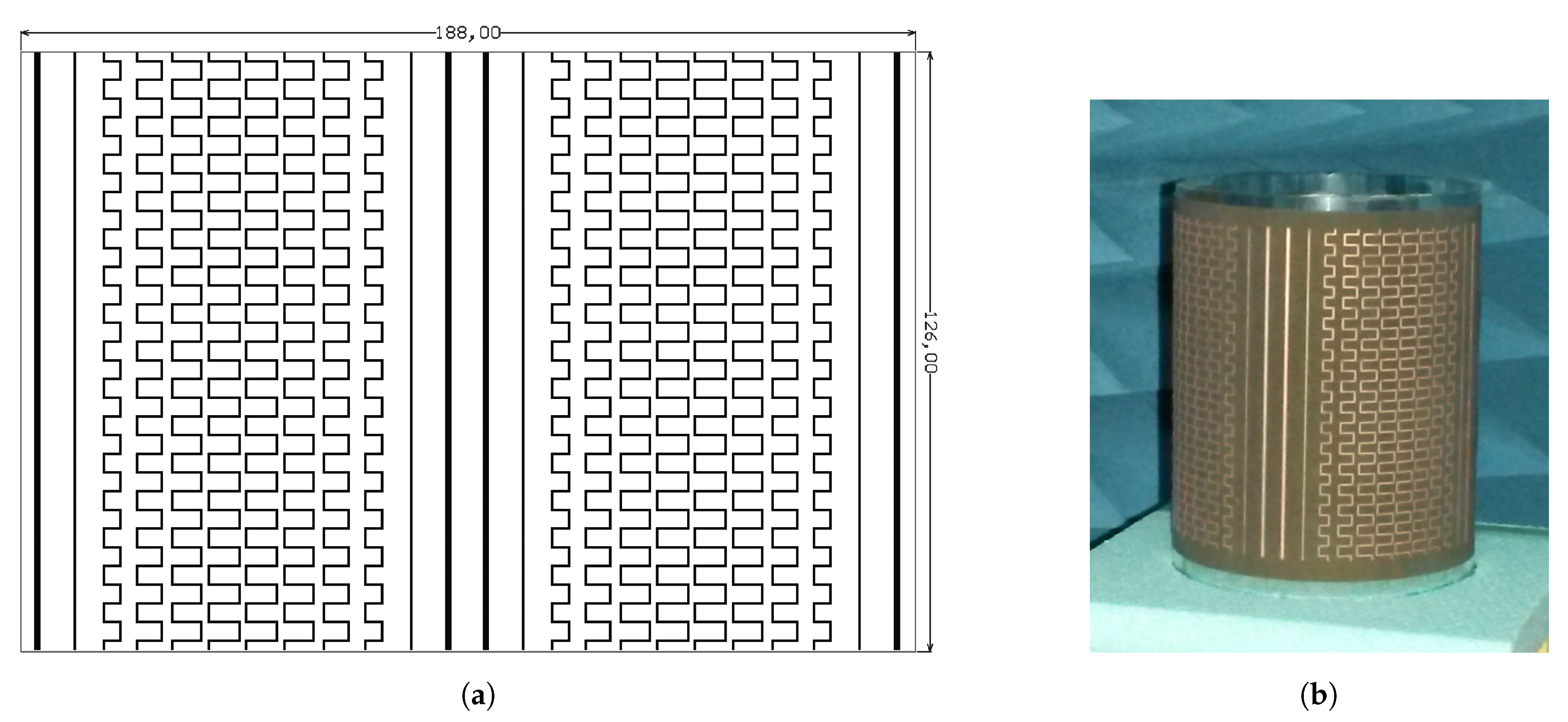
The MTS was produced in PCB technology. Figure 13a presents the positive mask used in the PCB production process. To measure its performance, the structure was placed in an anechoic chamber, as seen in Figure 13b. For measurements on the y-polarization, a monopole antenna was placed at the center of the structure (view obstructed by the MTS in the photograph), parallel to the strips on the MTS to produce a y-polarized wave. This antenna was to be used for transmitting, to excite the MTS with an unmodulated signal. The MTS is mounted on top of a rotating computer-controlled pole, and a receiving antenna is placed at the far edge of the anechoic chamber.
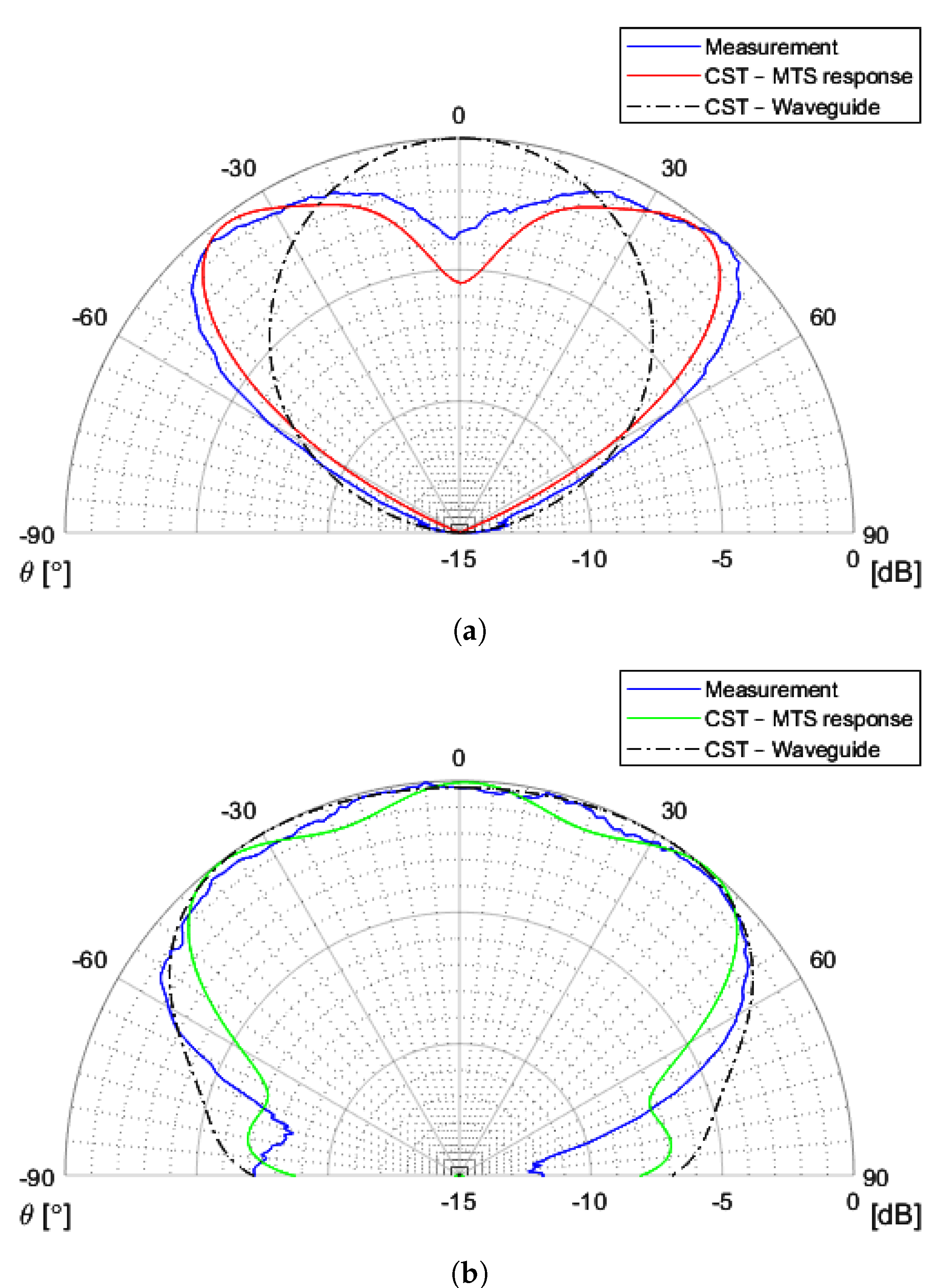
Measurement results are presented in Figure 14 with comparison to the expected response from Figure 12.
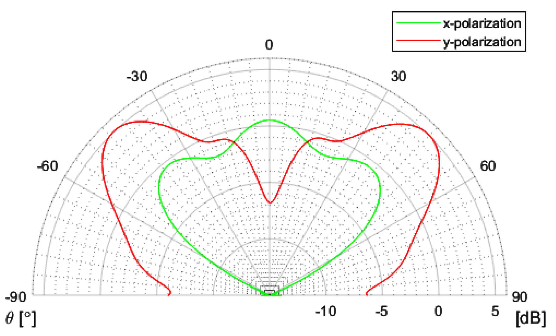
For x-polarization, measurement setup had to be altered, as the x-oriented monopole antenna would not illuminate the inner side of the MTS evenly. Therefore, x-polarization measurements were performed using a WR90 waveguide opening as the signal source. Measurements for y-polarization were repeated with the waveguide. Figure 15 presents the measured responses, as well as the simulated radiation pattern of the waveguide opening for reference.
The results show that the most significant response is observed for the y-polarized source, as intended by the design. While the response for x-polarization is not fully flat (as it ideally should be), the ripples are only around 1 dB in depth, in measurement results as well as in the simulated expected response.
6. Conclusions
Throughout this paper we gave an overview of approximate expressions for determining the sheet impedance and phase offsets achievable by different metallic patterns. The performance of these expressions has been compared to the performance of these unit cell designs in a full-wave electromagnetic simulator. For many designs, slight errors have been detected when comparing the analytical and simulated numerical results, and a simple optimization procedure has been suggested to correct for it. We have shown that a large range of sheet impedances can be achieved by utilizing only a handful of design patterns. The entire approach was confirmed by a developed metasurface intended for beam shaping, which shows good conformance of measured results to the expected response, as obtained by simulation in a commercial full-wave electromagnetic solver.
The work presented in this paper is equally applicable to any operating frequency, as long as the manufacturing capabilities enable precise production of unit cells. Limitations and guidelines for the design process have been discussed. The discussions on unit cell design are therefore beneficial to all multi-disciplinary fields working with metasurfaces.
Author Contributions
Conceptualization, D.B. and Z.Š.; methodology, D.B.; software, D.B.; validation, Z.Š.; formal analysis, D.B.; investigation, D.B.; resources, Z.Š.; data curation, D.B.; writing–original draft preparation, D.B.; writing–review and editing, Z.Š.; visualization, D.B.; supervision, Z.Š.; project administration, Z.Š. All authors have read and agreed to the published version of the manuscript.
Funding
This research received no external funding.
Acknowledgments
This work was supported in part by the Croatian Science Foundation under the project IP-2018-01-9753; and by Ericsson Nikola Tesla d.d. and the University of Zagreb Faculty of Electrical Engineering and Computing under the EWITA project.
Conflicts of Interest
The authors declare no conflict of interest.
Abbreviations
The following abbreviations are used in this manuscript:
| 2D | 2-dimensional |
| CAD | computer-aided design |
| EM | electromagnetic |
| GSTC | Generalized Sheet Transition Condition |
| MTS | metasurface |
| PCB | printed circuit board |
| S-parameters | scattering parameters |
References
- Holloway, C.L.; Kuester, E.F.; Gordon, J.A.; O’Hara, J.; Booth, J.; Smith, D.R. An Overview of the Theory and Applications of Metasurfaces: The Two-Dimensional Equivalents of Metamaterials. IEEE Antennas Propag. Mag. 2012, 54, 10–35. [Google Scholar] [CrossRef]
- Faenzi, M.; Minatti, G.; González-Ovejero, D.; Caminita, F.; Martini, E.; Della Giovampaola, C.; Maci, S. Metasurface Antennas: New Models, Applications and Realizations. Sci. Rep. 2019, 9, 10178. [Google Scholar] [CrossRef] [PubMed] [Green Version]
- Pfeiffer, C.; Grbic, A. Cascaded Metasurfaces for Complete Phase and Polarization Control. Appl. Phys. Lett. 2013, 102, 231116. [Google Scholar] [CrossRef]
- Pfeiffer, C.; Grbic, A. Bianisotropic Metasurfaces for Optimal Polarization Control: Analysis and Synthesis. Phys. Rev. Appl. 2014, 2, 044011. [Google Scholar] [CrossRef]
- Pfeiffer, C.; Grbic, A. Metamaterial Huygens’ Surfaces: Tailoring Wave Fronts with Reflectionless Sheets. Phys. Rev. Lett. 2013, 110, 197401. [Google Scholar] [CrossRef] [PubMed]
- Selvanayagam, M.; Eleftheriades, G.V. Discontinuous Electromagnetic Fields Using Orthogonal Electric and Magnetic Currents for Wavefront Manipulation. Opt. Express 2013, 21, 14409–14429. [Google Scholar] [CrossRef] [PubMed]
- Quevedo-Teruel, O.; Chen, H.; Díaz-Rubio, A.; Gok, G.; Grbic, A.; Minatti, G.; Martini, E.; Maci, S.; Eleftheriades, G.V.; Chen, M.; et al. Roadmap on Metasurfaces. J. Opt. 2013, 21, 073002. [Google Scholar] [CrossRef]
- Kuester, E.F.; Mohamed, M.A.; Piket-May, M.; Holloway, C.L. Averaged Transition Conditions for Electromagnetic Fields at a Metafilm. IEEE Trans. Antennas Propag. 2003, 51, 2641–2651. [Google Scholar] [CrossRef]
- Epstein, A.; Eleftheriades, G.V. Arbitrary Power-Conserving Field Transformations with Passive Lossless Omega-Type Bianisotropic Metasurfaces. IEEE Trans. Antennas Propag. 2016, 64, 3880–3895. [Google Scholar] [CrossRef] [Green Version]
- Pfeiffer, C.; Grbic, A. Millimeter-Wave Transmitarrays for Wavefront and Polarization Control. IEEE Trans. Microw. Theory Tech. 2013, 61, 4407–4417. [Google Scholar] [CrossRef]
- Šipuš, Z.; Bosiljevac, M.; Grbic, A. Modelling Cascaded Cylindrical Metasurfaces Using Sheet Impedances and a Transmission Matrix Formulation. IET Microw. Antennas Propag. 2018, 12, 1041–1047. [Google Scholar] [CrossRef]
- Tretyakov, S. Analytical Modeling in Applied Electromagnetics; Artech House: Boston, MA, USA, 2003. [Google Scholar]
- Luukkonen, O.; Simovski, C.; Granet, G.; Goussetis, G.; Lioubtchenko, D.; Räisänen, A.V.; Tretyakov, S.A. Simple and Accurate Analytical Model of Planar Grids and High-Impedance Surfaces Comprising Metal Strips or Patches. IEEE Trans. Antennas Propag. 2008, 56, 1624–1632. [Google Scholar] [CrossRef] [Green Version]
- Padooru, Y.R.; Yakovlev, A.B.; Chen, P.Y.; Alù, A. Analytical Modeling of Conformal Mantle Cloaks for Cylindrical Objects Using Sub-Wavelength Printed and Slotted Arrays. J. Appl. Phys. 2012, 112, 034907. [Google Scholar] [CrossRef] [Green Version]
- Born, M.; Wolf, E.; Bhatia, A.B.; Clemmow, P.C.; Gabor, D.; Stokes, A.R.; Taylor, A.M.; Wayman, P.A.; Wilcock, W.L. Principles of Optics: Electromagnetic Theory of Propagation, Interference and Diffraction of Light, 7th ed.; Cambridge University Press: Cambridge, UK, 1999. [Google Scholar]
- Langley, R.; Parker, E. Equivalent Circuit Model for Arrays of Square Loops. Electron. Lett. 1982, 18, 294–296. [Google Scholar] [CrossRef]
- Chu, R.S.; Lee, K.M. Analytical Model of a Multilayered Meander-Line Polarizer Plate with Normal and Oblique Plane-Wave Incidence. IEEE Trans. Antennas Propag. 1987, 35, 652–661. [Google Scholar] [CrossRef]
- CST Studio Suite. Dassault Systèmes. Available online: https://www.3ds.com/products-services/simulia/products/cst-studio-suite/ (accessed on 31 August 2020).
- Šipuš, Z.; Ereš, Z.; Barbarić, D. Modeling Cascaded Cylindrical Metasurfaces with Spatially-Varying Impedance Distribution. Radioengineering 2019, 28, 505–511. [Google Scholar] [CrossRef]
- Šipuš, Z.; Barbarić, D.; Bosiljevac, M. Analysis of Curved Metasurfaces with Spatially-Varying Impedance Distribution. In Proceedings of the 13th European Conference on Antennas and Propagation (EuCAP), Krakow, Poland, 31 March–5 April 2019. [Google Scholar]
- Barbarić, D.; Bosiljevac, M.; Šipuš, Z. Analysis of Curved Metasurfaces Based on Method of Moments. In Proceedings of the 14th European Conference on Antennas and Propagation (EuCAP), Copenhagen, Denmark, 15–20 March 2020. [Google Scholar]
- Barbarić, D.; Šipuš, Z. Synthesis of Curved Beam-Shaping Metasurfaces. In Proceedings of the IEEE International Symposium on Antennas and Propagation and USNC-URSI Radio Science Meeting, Montréal, QC, Canada, 5–10 July 2020. [Google Scholar]
Figure 1.
Unit cell geometry with obliquely-incident plane wave excitation. The image displays a TE-incident wave, with residing in the plane. A TM-incident wave would have and swapped in this image.
Figure 1.
Unit cell geometry with obliquely-incident plane wave excitation. The image displays a TE-incident wave, with residing in the plane. A TM-incident wave would have and swapped in this image.
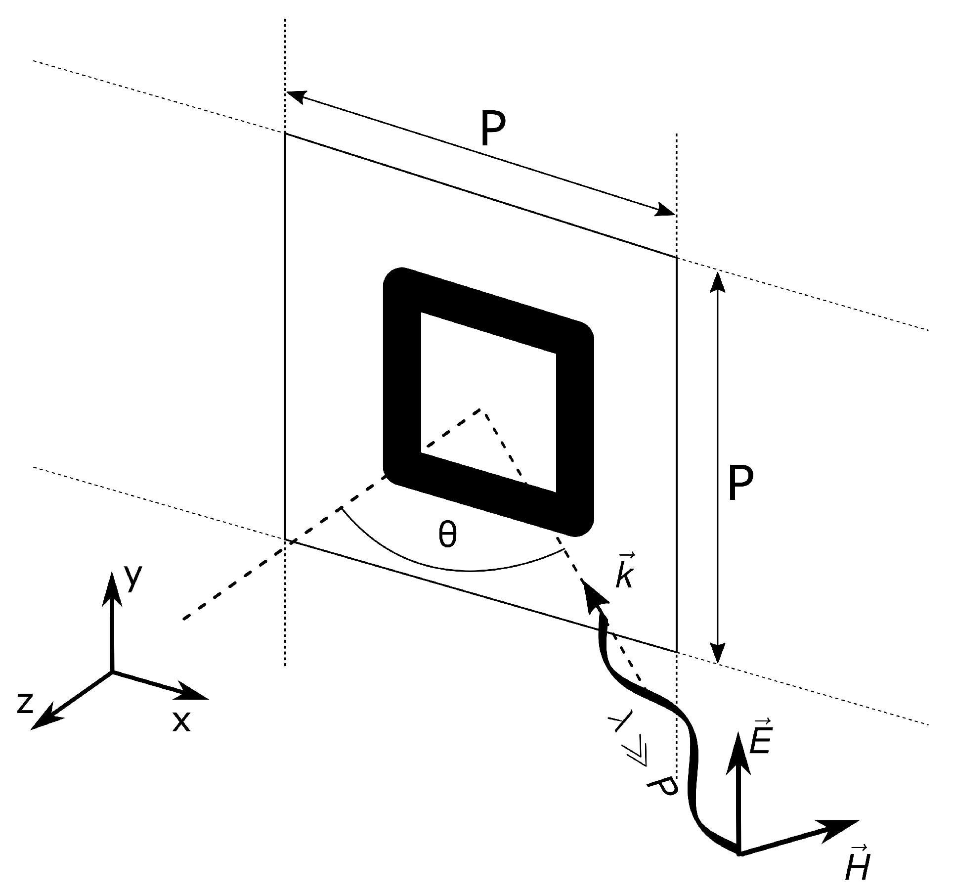
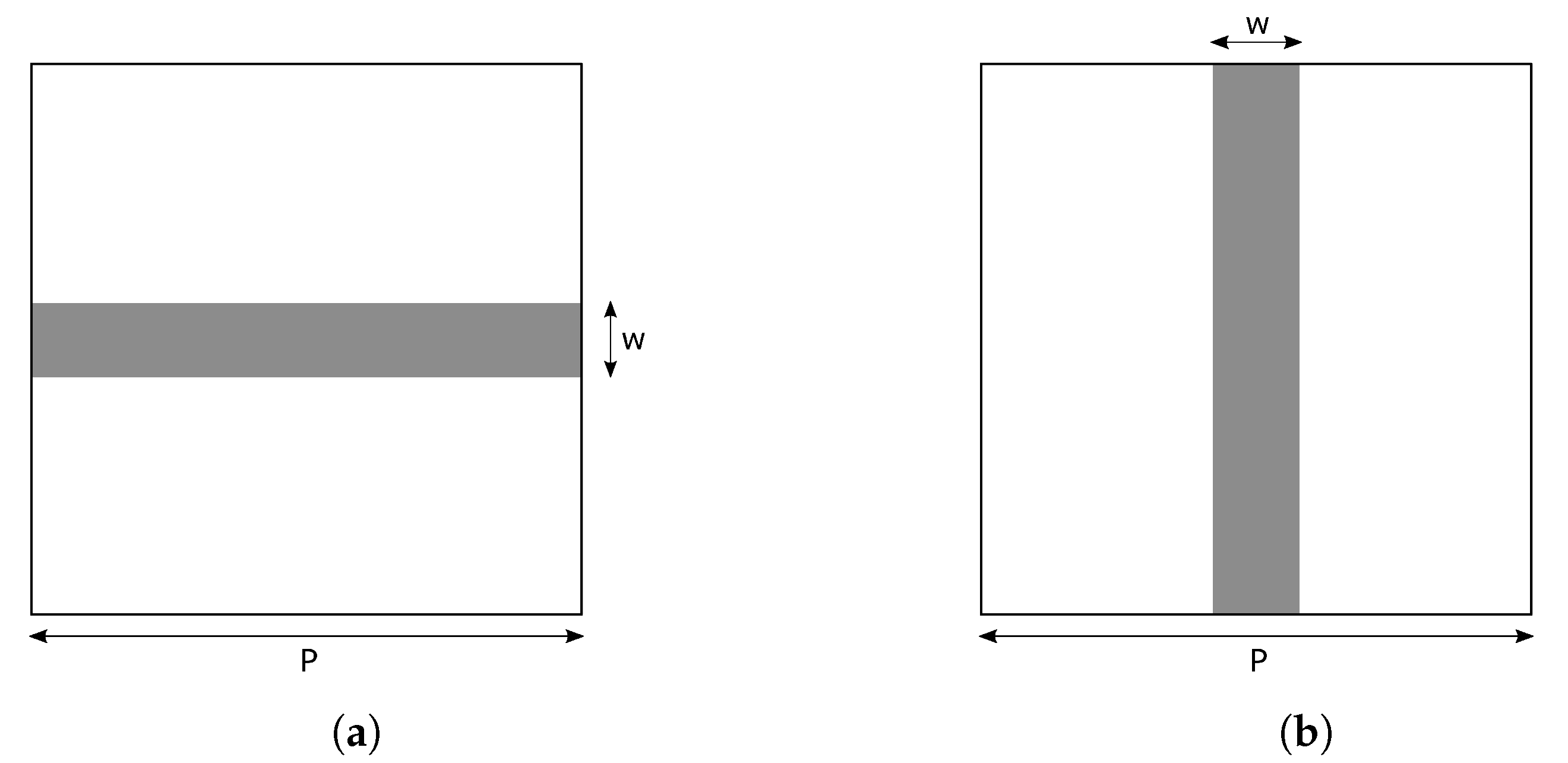
Figure 2.
Geometry of strip unit cells. (a) Perpendicular strip unit cell; (b) parallel strip unit cell.
Figure 2.
Geometry of strip unit cells. (a) Perpendicular strip unit cell; (b) parallel strip unit cell.

Figure 3.
Geometry of patch-based unit cells. (a) Patch unit cell; (b) loop unit cell.

Figure 4.
Geometry of meander line unit cells.
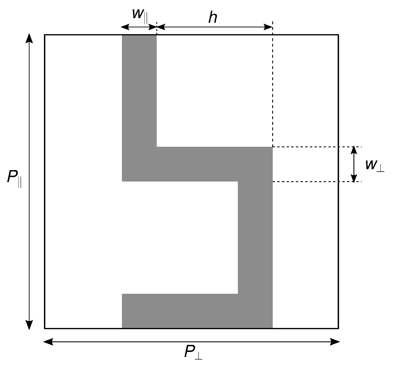
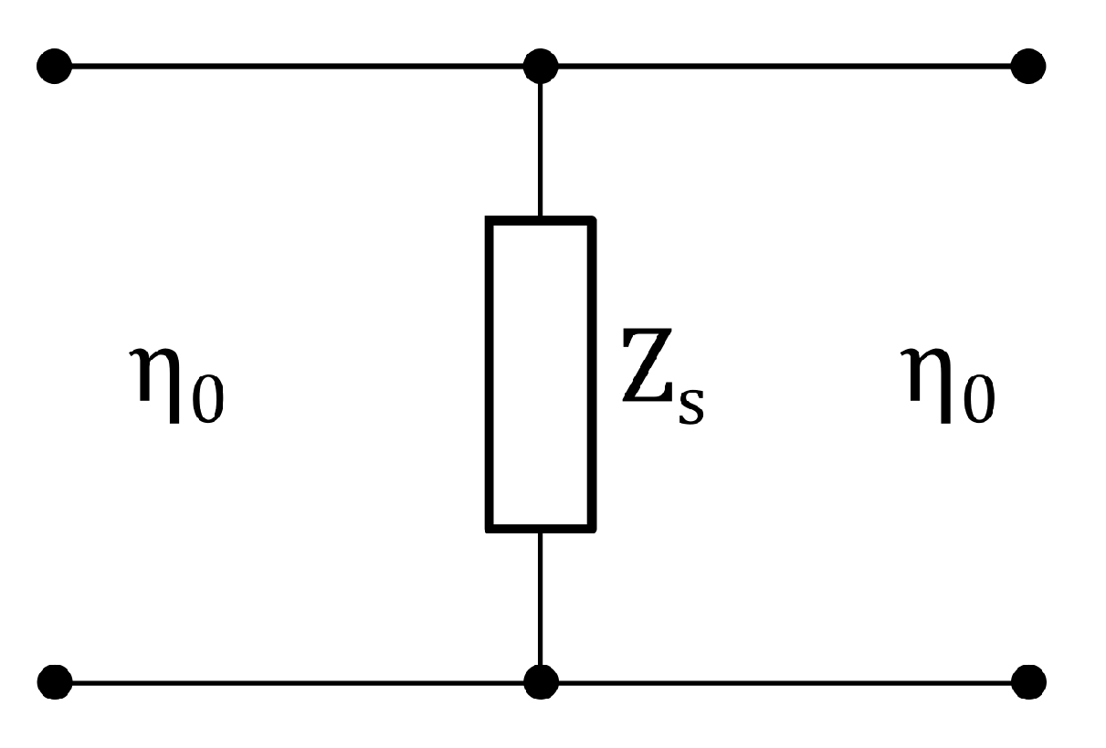
Figure 5.
Tranmission-line equivalent circuit of an MTS layer, presented by surface sheet impedance , placed in free space, and excited by a normally-incident wave.
Figure 5.
Tranmission-line equivalent circuit of an MTS layer, presented by surface sheet impedance , placed in free space, and excited by a normally-incident wave.

Figure 6.
Performance of strip unit cells. Lines are analysis, points simulation results. Solid and circles—parallel strip; dashed and crosses—perpendicular strip. (a) Surface reactance; (b) phase shift.
Figure 6.
Performance of strip unit cells. Lines are analysis, points simulation results. Solid and circles—parallel strip; dashed and crosses—perpendicular strip. (a) Surface reactance; (b) phase shift.

Figure 7.
Performance of patch unit cells. Lines are analysis, points simulation results. (a) Surface reactance; (b) phase shift.
Figure 7.
Performance of patch unit cells. Lines are analysis, points simulation results. (a) Surface reactance; (b) phase shift.
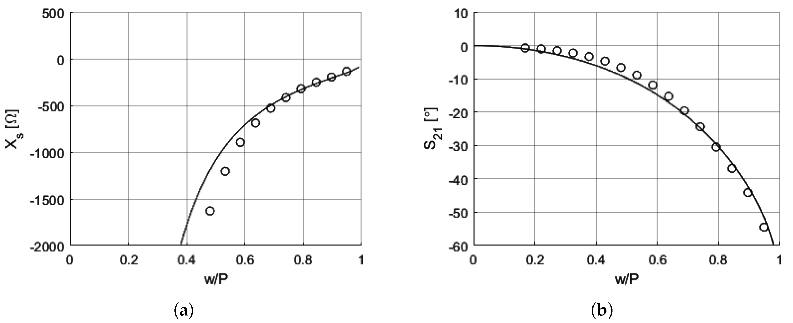
Figure 8.
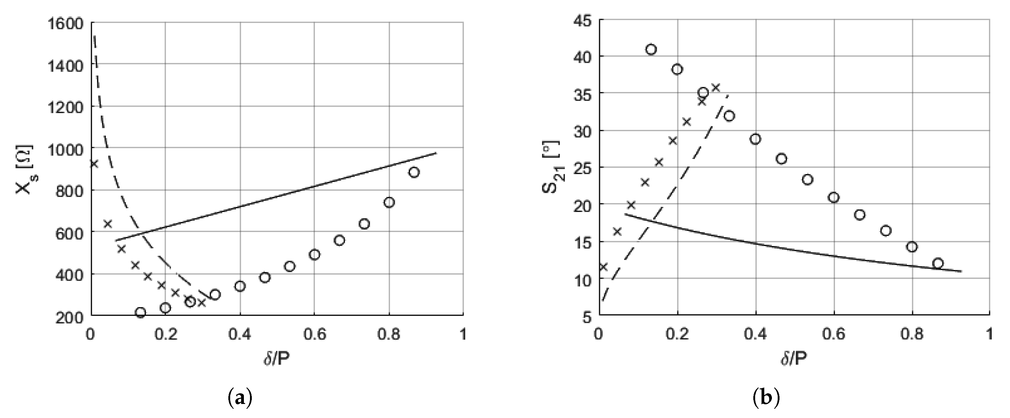
Performance of loop unit cells. Lines are analysis, points simulation results. Solid and circles—δ ~ d, w = P/15; dashed and crosses—δ ~ w, d = 2P/3. (a) Surface reactance; (b) phase shift.
Figure 8.
Performance of loop unit cells. Lines are analysis, points simulation results. Solid and circles—δ ~ d, w = P/15; dashed and crosses—δ ~ w, d = 2P/3. (a) Surface reactance; (b) phase shift.

Figure 9.
Performance of meander line unit cells. P⊥ = P‖ = P. Lines are analysis, points simulation results. Solid and circles—δ ~ h, w‖ = w⊥ = P⊥/15; dashed and crosses—δ ~ w‖ = w⊥, h = 2 P⊥/3. (a) Surface reactance; (b) phase shift.
Figure 9.
Performance of meander line unit cells. P⊥ = P‖ = P. Lines are analysis, points simulation results. Solid and circles—δ ~ h, w‖ = w⊥ = P⊥/15; dashed and crosses—δ ~ w‖ = w⊥, h = 2 P⊥/3. (a) Surface reactance; (b) phase shift.

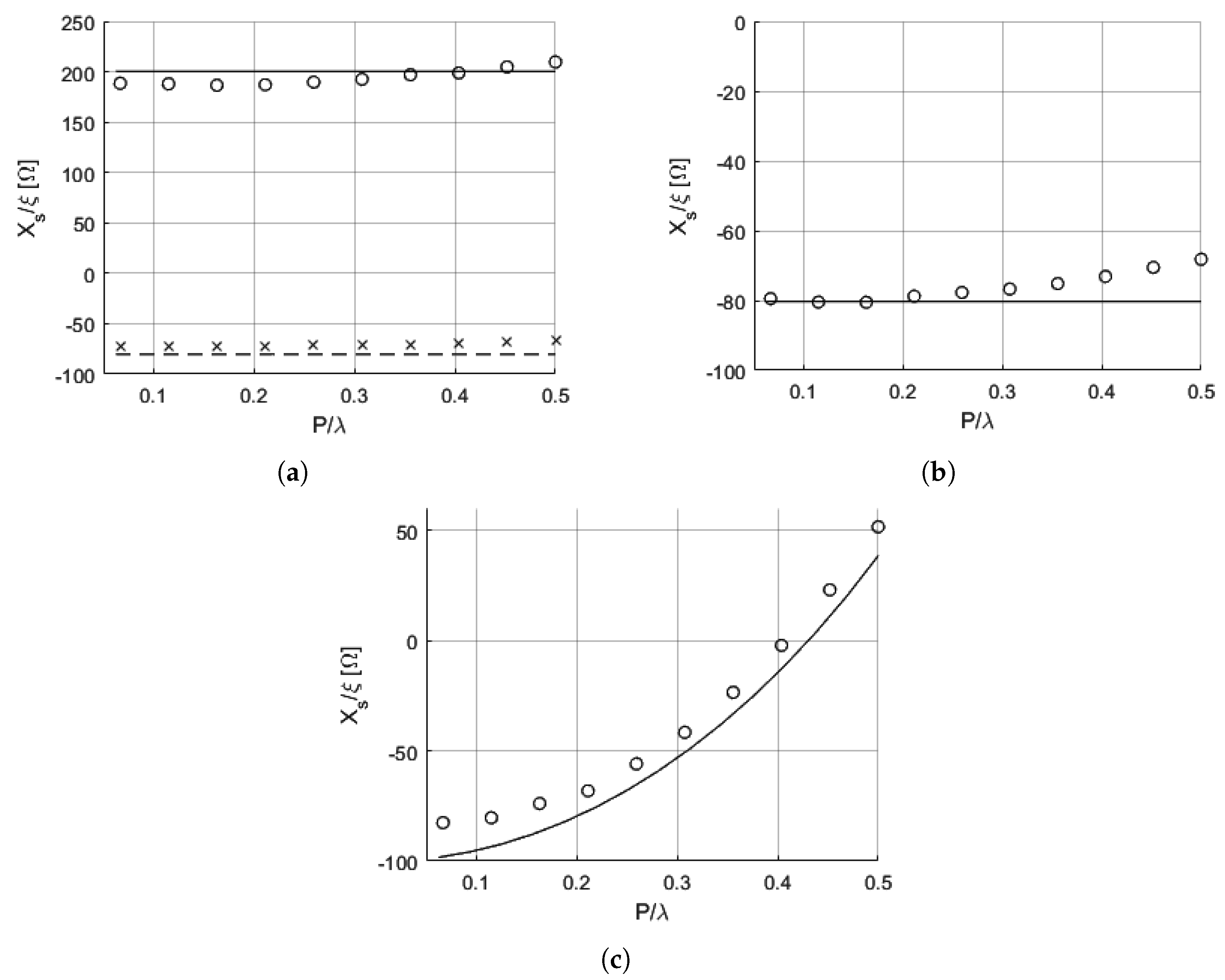
Figure 10.
Performance of unit cells over the unit cell period. (a) Strips. Solid and circles—Inductive vertical strips, w = 4 P/10; dashed and crosses—capacitive horizontal strips, w = 8 P/10; (b) capacitive patches, w = 8 P/10; (c) predominantly capacitive loops, w = P/15, d = 8 P/10.
Figure 10.
Performance of unit cells over the unit cell period. (a) Strips. Solid and circles—Inductive vertical strips, w = 4 P/10; dashed and crosses—capacitive horizontal strips, w = 8 P/10; (b) capacitive patches, w = 8 P/10; (c) predominantly capacitive loops, w = P/15, d = 8 P/10.

Figure 11.
Comparison of electrical parameters for different unit cell types for a y-polarized normally-incident wave. P = 7.854 mm, f = 10 GHz. (a) Surface sheet reactances; (b) phase shifts.
Figure 11.
Comparison of electrical parameters for different unit cell types for a y-polarized normally-incident wave. P = 7.854 mm, f = 10 GHz. (a) Surface sheet reactances; (b) phase shifts.

Figure 12.
Simulated response of the prototype semi-cylindrical metasurface (MTS).

Figure 13.
Produced semi-cylindrical MTS. (a) Positive printed circuit board (PCB) production mask. Dimensions are in mm; (b) the MTS in the measurement environment.
Figure 13.
Produced semi-cylindrical MTS. (a) Positive printed circuit board (PCB) production mask. Dimensions are in mm; (b) the MTS in the measurement environment.

Figure 14.
Simulated and measured response of a produced semi-cylindrical MTS, with a y-oriented short dipole as the source. Normalized to maximum directivity.
Figure 14.
Simulated and measured response of a produced semi-cylindrical MTS, with a y-oriented short dipole as the source. Normalized to maximum directivity.
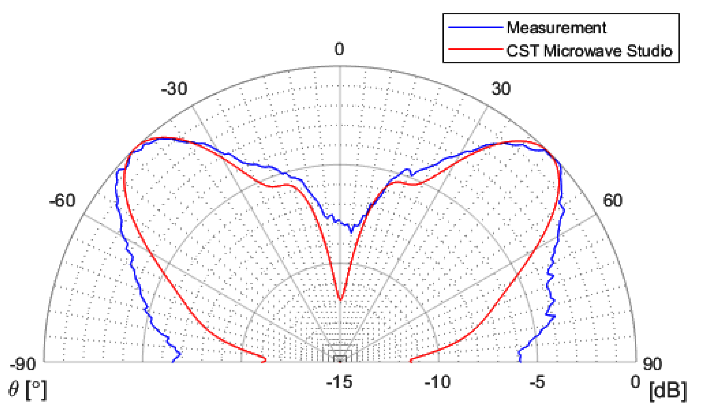
Figure 15.
Simulated and measured response of a produced semi-cylindrical MTS, with a WR90 waveguide opening as the source. Normalized to maximum directivity. (a) y-oriented waveguide opening; (b) x-oriented waveguide opening.
Figure 15.
Simulated and measured response of a produced semi-cylindrical MTS, with a WR90 waveguide opening as the source. Normalized to maximum directivity. (a) y-oriented waveguide opening; (b) x-oriented waveguide opening.


Table 1.
Design parameters of a semi-cylindrical metasurface. Numeration starts at the edge of the structure.
Table 1.
Design parameters of a semi-cylindrical metasurface. Numeration starts at the edge of the structure.
| Element No. | Unit Cell Type | Fixed Design Parameter | Initial Design Parameter | Optimized Design Parameter | Sheet Reactance for |
|---|---|---|---|---|---|
| 1 | Strip | – | w = 1.30 mm | w = 1.30 mm | |
| 2 | Strip | – | w = 0.50 mm | w = 0.50 mm | |
| 3 | Meander | w = 0.50 mm | h = 1.53 mm | h = 3.00 mm | |
| 4 | Meander | w = 0.50 mm | h = 3.33 mm | h = 4.65 mm | |
| 5 | Meander | w = 0.50 mm | h = 4.89 mm | h = 5.60 mm | |
| 6 | Meander | w = 0.50 mm | h = 5.79 mm | h = 6.00 mm |
Publisher’s Note: MDPI stays neutral with regard to jurisdictional claims in published maps and institutional affiliations. |
© 2020 by the authors. Licensee MDPI, Basel, Switzerland. This article is an open access article distributed under the terms and conditions of the Creative Commons Attribution (CC BY) license (http://creativecommons.org/licenses/by/4.0/).
Share and Cite
MDPI and ACS Style
Barbarić, D.; Šipuš, Z. Designing Metasurfaces with Canonical Unit Cells. Crystals 2020, 10, 938. https://doi.org/10.3390/cryst10100938
AMA Style
Barbarić D, Šipuš Z. Designing Metasurfaces with Canonical Unit Cells. Crystals. 2020; 10(10):938. https://doi.org/10.3390/cryst10100938
Chicago/Turabian StyleBarbarić, Dominik, and Zvonimir Šipuš. 2020. "Designing Metasurfaces with Canonical Unit Cells" Crystals 10, no. 10: 938. https://doi.org/10.3390/cryst10100938
Note that from the first issue of 2016, this journal uses article numbers instead of page numbers. See further details here.