Anisotropic Strain on GaN Microdisks Grown by Plasma-Assisted Molecular Beam Epitaxy

 ,
, 
Abstract
1. Introduction
2. Materials and Methods
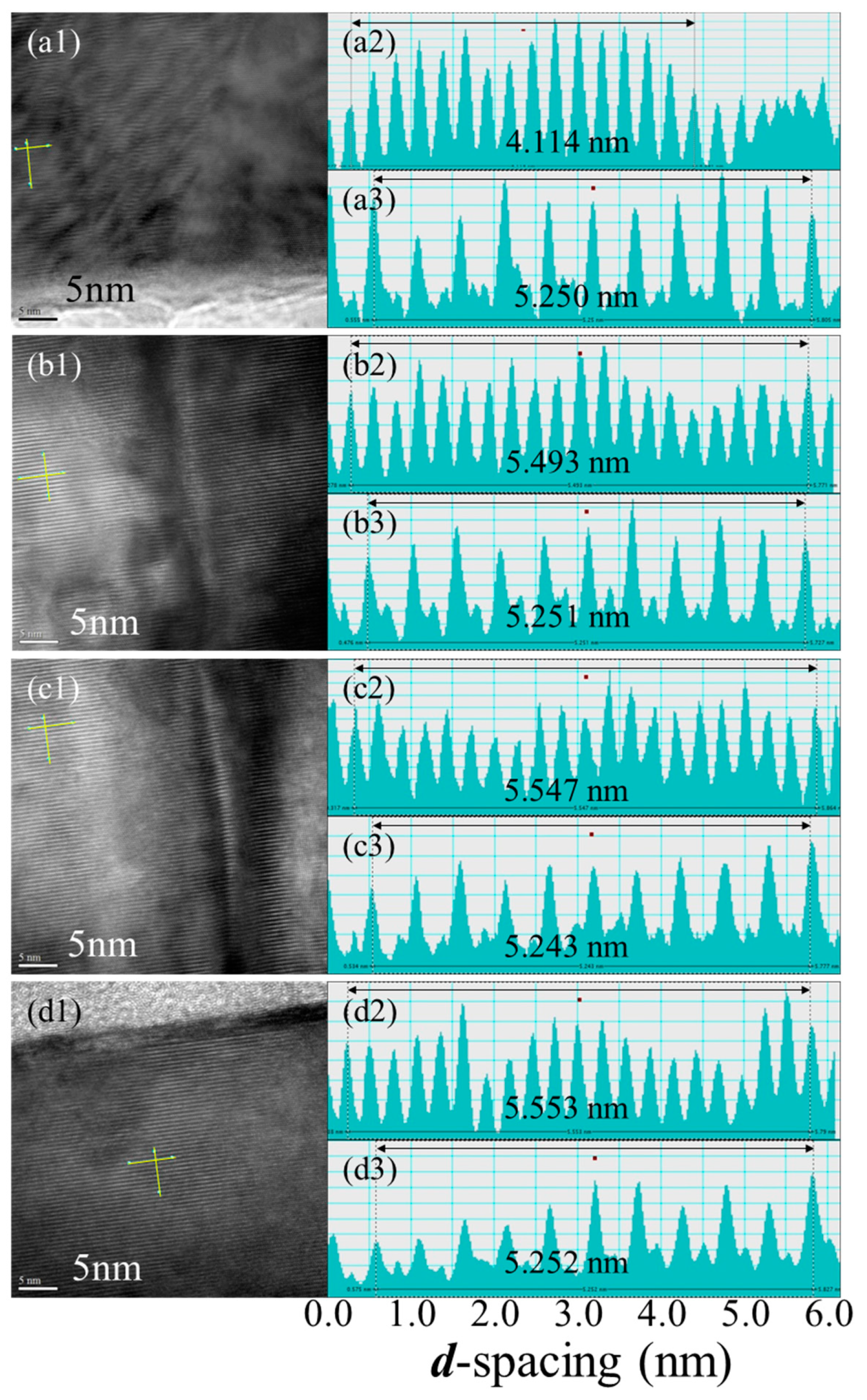
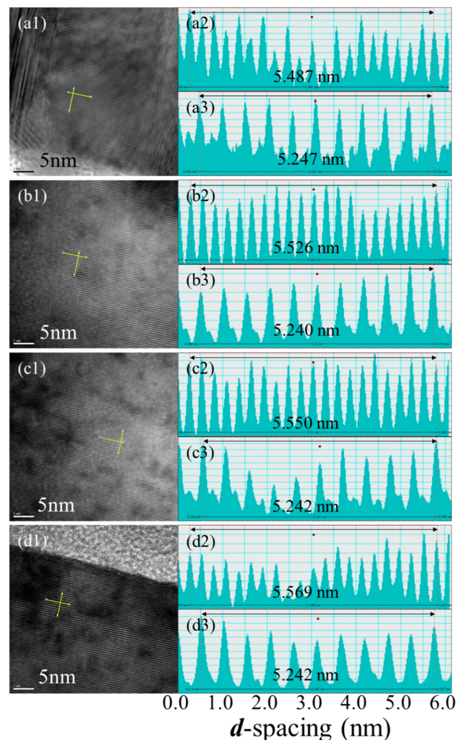
3. Results and Discussion
4. Conclusions
Author Contributions
Funding
Acknowledgments
Conflicts of Interest
References
- Lo, I.; Tsai, J.K.; Yao, W.J.; Ho, P.C.; Tu, L.-W.; Chang, T.C.; Elhamri, S.; Mitchel, W.C.; Hsieh, K.Y.; Huang, J.H.; et al. Spin splitting in modulation-dopedAlxGa1−xN/GaNheterostructures. Phys. Rev. B 2002, 65, 161306. [Google Scholar] [CrossRef]
- Lo, I.; Wang, W.T.; Gau, M.H.; Tsay, S.F.; Chiang, J.C. Wurtzite structure effects on spin splitting inGaN∕AlNquantum wells. Phys. Rev. B 2005, 72, 245329. [Google Scholar] [CrossRef]
- Nakamura, S.; Senoh, M.; Iwasa, N.; Nagahama, S.-I.; Yamada, T.; Mukai, T. Superbright Green InGaN Single-Quantum-Well-Structure Light-Emitting Diodes. Jpn. J. Appl. Phys. 1995, 34, L1332. [Google Scholar] [CrossRef]
- Nakamura, S.; Pearton, S.; Fasol, G. The Blue Laser Diode, 2nd ed.; Springer: Berlin, Germany, 2000. [Google Scholar]
- Madelung, O. Data in Science and Technology, Semiconductors Group IV Elements and III-V Compounds; Springer: Berlin, Germany, 1991. [Google Scholar]
- Morkoc, H.; Strite, S.; Gao, G.B.; Lin, M.E.; Sverdlov, B.; Burns, M. Large-band-gap SiC, III-V nitride, and II-VI ZnSe-based semiconductor device technologies. J. Appl. Phys. 1994, 76, 1363. [Google Scholar] [CrossRef]
- Wu, J.; Walukiewicz, W.; Yu, K.M.; Ager, J.W.; Haller, E.E.; Lu, H.; Schaff, W.J.; Saito, Y.; Nanishi, Y. Unusual properties of the fundamental band gap of InN. Appl. Phys. Lett. 2002, 80, 3967–3969. [Google Scholar] [CrossRef]
- Wu, J.; Walukiewicz, W.; Shan, W.; Yu, K.M.; Ager, J.W.; Li, S.X.; Haller, E.E.; Lu, H.; Schaff, W.J. Temperature dependence of the fundamental band gap of InN. J. Appl. Phys. 2003, 94, 4457–4460. [Google Scholar] [CrossRef]
- Lo, I.; Hsieh, C.-H.; Hsu, Y.-C.; Pang, W.-Y.; Chou, M.-C. Self-assembled GaN hexagonal micropyramid and microdisk. Appl. Phys. Lett. 2009, 94, 062105. [Google Scholar] [CrossRef]
- Tsai, C.-D.; Lo, I.; Wang, Y.-C.; Yang, C.-C.; You, S.-T.; Yang, H.-Y.; Huang, H.-C.; Chou, M.M.C. Finite growth of InGaN/GaN triple-quantum-well microdisks on LiAlO2 substrate. AIP Adv. 2018, 8, 095208. [Google Scholar] [CrossRef]
- Tsai, C.; Lo, I.; Wang, Y.; Yang, C.; Yang, H.; Shih, H.; Huang, H.; Chou, M.M.C.; Huang, L.; Tseng, B. Indium-Incorporation with InxGa1−xN Layers on GaN-Microdisks by Plasma-Assisted Molecular Beam Epitaxy. Crystals 2019, 9, 308. [Google Scholar] [CrossRef]
- Lo, I.; Wang, Y.-C.; Hsu, Y.-C.; Shih, C.-H.; Pang, W.-Y.; You, S.-T.; Hu, C.-H.; Chou, M.M.C.; Hsu, G.Z.L. Electrical contact for wurtzite GaN microdisks. Appl. Phys. Lett. 2014, 105, 082101. [Google Scholar]
- Waltereit, P.; Brandt, O.; Trampert, A.; Grahn, H.T.; Menniger, J.; Ramsteiner, M.; Reiche, M.; Ploog, K.H. Nitride semiconductors free of electrostatic fields for efficient white light-emitting diodes. Nat. Cell Biol. 2000, 406, 865–868. [Google Scholar] [CrossRef] [PubMed]
- Hsieh, C.H.; Lo, I.; Gau, M.H.; Chen, Y.L.; Chou, M.C.; Pang, W.Y.; Chang, Y.I.; Hsu, Y.C.; Sham, M.W.; Chiang, J.C.; et al. Self-assembled c-plane GaN nanopillars on γ-LiAlO2 substrate grown by plasma-assisted molecular-beam epitaxy. Jpn. J. App. Phys. 2008, 47, 891. [Google Scholar] [CrossRef]
- Reshchikov, M.A.; Morkoç, H. Luminescence properties of defects in GaN. J. Appl. Phys. 2005, 97, 061301. [Google Scholar] [CrossRef]
- Reshchikov, M.A.; Huang, D.; Yun, F.; He, L.; Morkoç, H.; Reynolds, D.C.; Park, S.S.; Lee, K.Y. Photoluminescence of GaN grown by molecular-beam epitaxy on a freestanding GaN template. Appl. Phys. Lett. 2001, 79, 3779–3781. [Google Scholar] [CrossRef]
- Díaz-Guerra, C.; Piqueras, J.; Volciuc, O.; Popa, V.; Tiginyanu, I.M. Cathodoluminescence microscopy and spectroscopy of GaN epilayers microstructured using surface charge lithography. J. Appl. Phys. 2006, 100, 023509. [Google Scholar] [CrossRef]


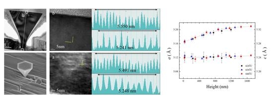
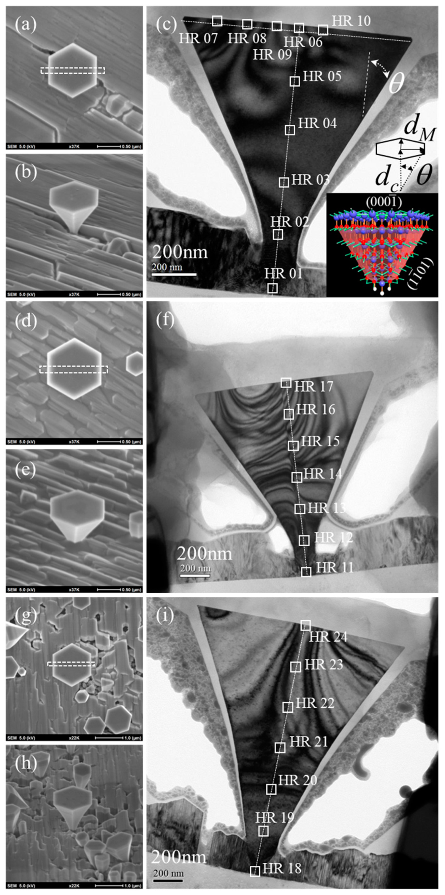
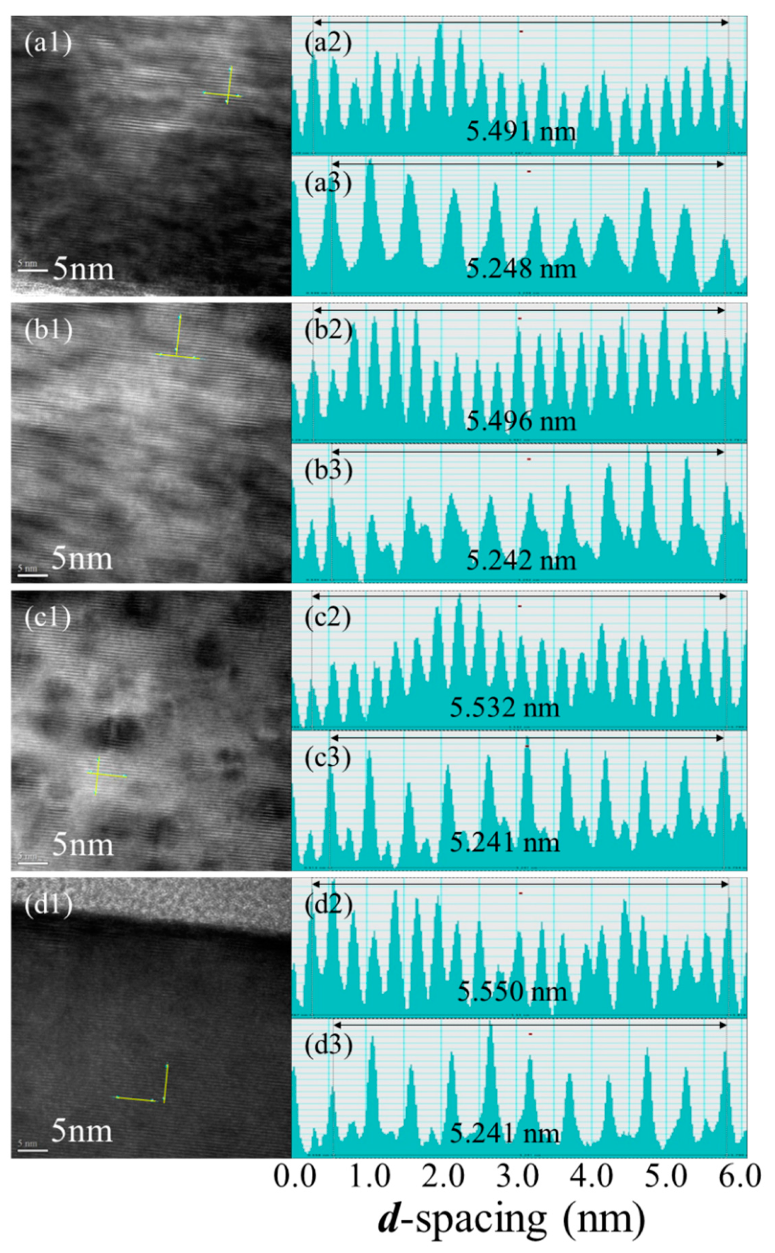
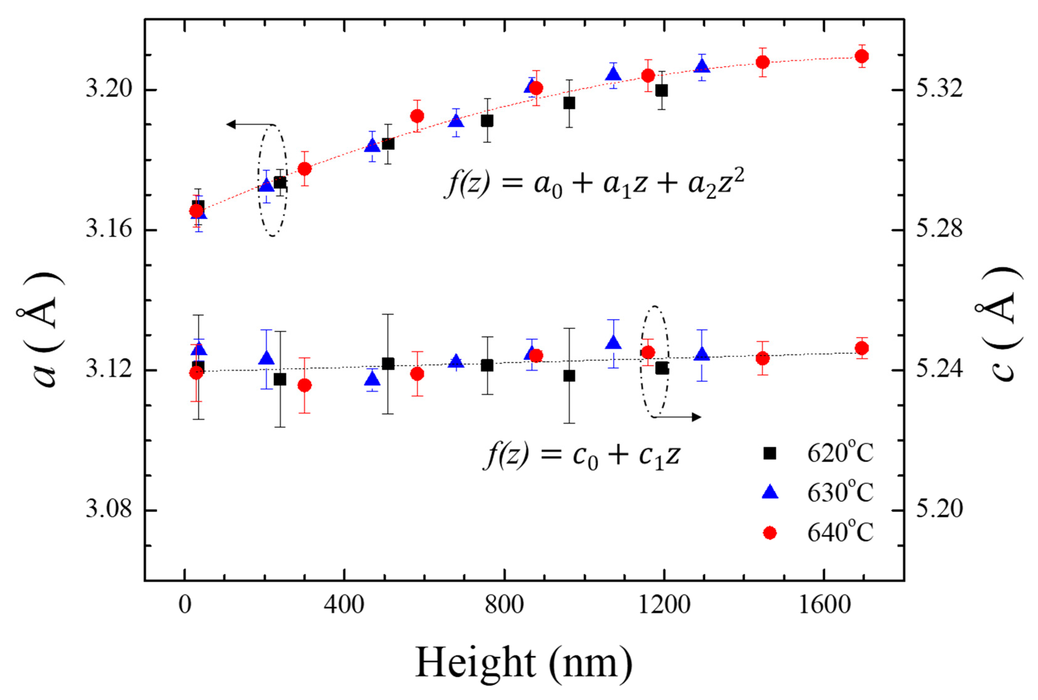
| Sample A | Lattice Constant a (Å) | Standard Deviation of a (Å) | Lattice Constant c (Å) | Standard Deviation of c (Å) |
|---|---|---|---|---|
| HR01 | 3.168 | 0.005 | 5.241 | 0.015 |
| HR02 | 3.174 | 0.004 | 5.237 | 0.014 |
| HR03 | 3.185 | 0.006 | 5.242 | 0.014 |
| HR04 | 3.191 | 0.006 | 5.241 | 0.008 |
| HR05 | 3.196 | 0.007 | 5.238 | 0.013 |
| HR06 | 3.200 | 0.005 | 5.241 | 0.002 |
| HR07 | 3.208 | 0.005 | 5.240 | 0.018 |
| HR08 | 3.201 | 0.009 | 5.244 | 0.010 |
| HR09 | 3.200 | 0.009 | 5.242 | 0.012 |
| HR10 | 3.194 | 0.013 | 5.241 | 0.011 |
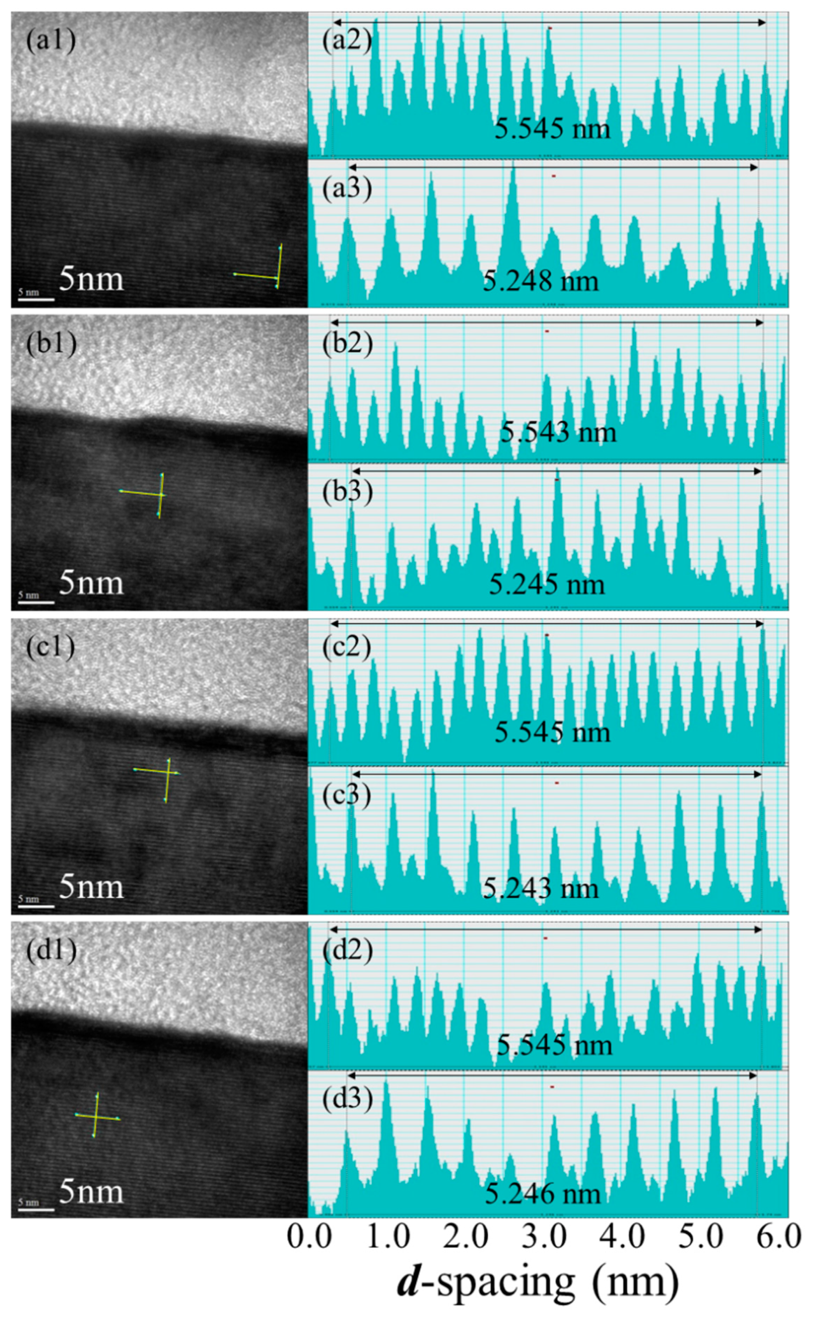
| Sample B | Lattice Constant a (Å) | Standard Deviation of a (Å) | Lattice Constant c (Å) | Standard Deviation of c (Å) |
|---|---|---|---|---|
| HR11 | 3.165 | 0.005 | 5.246 | 0.003 |
| HR12 | 3.172 | 0.005 | 5.243 | 0.008 |
| HR13 | 3.184 | 0.004 | 5.237 | 0.003 |
| HR14 | 3.191 | 0.004 | 5.242 | 0.001 |
| HR15 | 3.201 | 0.003 | 5.245 | 0.004 |
| HR16 | 3.204 | 0.004 | 5.248 | 0.007 |
| HR17 | 3.206 | 0.004 | 5.244 | 0.007 |
| Sample C | Lattice Constant a (Å) | Standard Deviation of a (Å) | Lattice Constant c (Å) | Standard Deviation of c (Å) |
|---|---|---|---|---|
| HR18 | 3.165 | 0.005 | 5.239 | 0.008 |
| HR19 | 3.178 | 0.005 | 5.236 | 0.008 |
| HR20 | 3.193 | 0.005 | 5.239 | 0.006 |
| HR21 | 3.200 | 0.005 | 5.244 | 0.001 |
| HR22 | 3.204 | 0.004 | 5.245 | 0.004 |
| HR23 | 3.208 | 0.004 | 5.243 | 0.005 |
| HR24 | 3.210 | 0.003 | 5.246 | 0.003 |
© 2020 by the authors. Licensee MDPI, Basel, Switzerland. This article is an open access article distributed under the terms and conditions of the Creative Commons Attribution (CC BY) license (http://creativecommons.org/licenses/by/4.0/).
Share and Cite
Yang, H.-Y.; Lo, I.; Tsai, C.-D.; Wang, Y.-C.; Shih, H.-J.; Huang, H.-C.; Chou, M.M.C.; Huang, L.; Wang, T.; Kuo, C.T.C. Anisotropic Strain on GaN Microdisks Grown by Plasma-Assisted Molecular Beam Epitaxy. Crystals 2020, 10, 899. https://doi.org/10.3390/cryst10100899
Yang H-Y, Lo I, Tsai C-D, Wang Y-C, Shih H-J, Huang H-C, Chou MMC, Huang L, Wang T, Kuo CTC. Anisotropic Strain on GaN Microdisks Grown by Plasma-Assisted Molecular Beam Epitaxy. Crystals. 2020; 10(10):899. https://doi.org/10.3390/cryst10100899
Chicago/Turabian StyleYang, Hong-Yi, Ikai Lo, Cheng-Da Tsai, Ying-Chieh Wang, Huei-Jyun Shih, Hui-Chun Huang, Mitch M. C. Chou, Louie Huang, Terence Wang, and Ching T. C. Kuo. 2020. "Anisotropic Strain on GaN Microdisks Grown by Plasma-Assisted Molecular Beam Epitaxy" Crystals 10, no. 10: 899. https://doi.org/10.3390/cryst10100899
APA StyleYang, H.-Y., Lo, I., Tsai, C.-D., Wang, Y.-C., Shih, H.-J., Huang, H.-C., Chou, M. M. C., Huang, L., Wang, T., & Kuo, C. T. C. (2020). Anisotropic Strain on GaN Microdisks Grown by Plasma-Assisted Molecular Beam Epitaxy. Crystals, 10(10), 899. https://doi.org/10.3390/cryst10100899