Article

Investigating the Impact of Stress on the Optical Properties of GaN-MX2 (M=Mo, W; X=S, Se) Heterojunctions Using the First Principles

1
Xinjiang Laboratory of Phase Transitions and Microstructures in Condensed Matters, College of Physical Science and Technology, Yili Normal University, Yining 835000, China
2
National Laboratory of Solid State Microstructures, Nanjing University, Nanjing 210093, China
3
Jiangsu Key Laboratory of Artificial Functional Materials, Department of Materials Science and Engineering, College of Engineering and Applied Sciences, Nanjing University, Nanjing 210093, China
*
Authors to whom correspondence should be addressed.
Catalysts 2024, 14(10), 732; https://doi.org/10.3390/catal14100732
Submission received: 20 September 2024 / Revised: 13 October 2024 / Accepted: 17 October 2024 / Published: 19 October 2024
(This article belongs to the Special Issue New Advances in Photocatalytic Hydrogen Production)

Abstract

:
This study used the first-principles-based CASTEP software to calculate the structural, electronic, and optical properties of heterojunctions based on single-layer GaN. GaN-MX2 exhibited minimal lattice mismatches, typically less than 3.5%, thereby ensuring lattice coherence. Notably, GaN-MoSe2 had the lowest binding energy, signifying its superior stability among the variants. When compared to single-layer GaN, which has an indirect band gap, all four heterojunctions displayed a smaller direct band gap. These heterojunctions were classified as type II. GaN-MoS2 and GaN-MoSe2 possessed relatively larger interface potential differences, hinting at stronger built-in electric fields. This resulted in an enhanced electron–hole separation ability. GaN-MoSe2 exhibited the highest value for the real part of the dielectric function. This suggests a superior electronic polarization capability under an electric field, leading to high electron mobility. GaN-MoSe2 possessed the strongest optical absorption capacity. Consequently, GaN-MoSe2 was inferred to possess the strongest photocatalytic capability. The band structure and optical properties of GaN-MoSe2 under applied pressure were further calculated. The findings revealed that stress significantly influenced the band gap width and light absorption capacity of GaN-MoSe2. Specifically, under a pressure of 5 GPa, GaN-MoSe2 demonstrated a significantly narrower band gap and enhanced absorption capacity compared to its intrinsic state. These results imply that the application of stress could potentially boost its photocatalytic performance, making it a promising candidate for various applications.

1. Introduction

In contemporary society, while individuals embrace the convenience bestowed by advanced technology, they are simultaneously confronted with grave environmental pollution issues [1,2,3,4]. Photocatalytic technology enables the conversion of solar energy into chemical energy and possesses the capability to degrade environmental pollutants. Therefore, extensive research has been conducted on various photocatalyst materials, including TiO2 [5], g-C3N4 [6], CdS [7], and GaN [8]. Among these, GaN has garnered significant attention from researchers due to its cost-effectiveness, facile preparation process, and exceptional catalytic activity [9]. However, the wide bandgap (approximately 3.4 eV [10]) of this material restricts its absorption range for solar radiation and poses a challenge to its practical implementation in everyday applications. Consequently, multiple enhancement techniques such as doping, defect engineering, and heterojunction formation have emerged successively [11]. By employing these technologies, the bandgap width of the system can be effectively reduced, thereby broadening the absorption spectrum range of solar radiation for the material and further augmenting its photocatalytic activity. Among these, the construction of heterojunctions facilitates catalysts to exhibit enhanced carrier mobility, thereby endowing them with remarkable visible light absorption capability and facilitating efficient electron–hole pair separation. Zhang et al. [12] theoretically investigated the electronic structure of GaN/AlN. The determined band gap width of the material was 2.44 eV, exhibiting a lower value compared to that of monolayer AlN (2.79 eV). This indicates that constructing heterojunctions can effectively reduce the band gap width of the system, increasing the probability of electron transitions. Fu et al. [13] conducted computational studies on the electronic structure and optical properties of monolayer g-C3N4 and the GaN/g-C3N4 heterojunction. They found that the band gap value of GaN/g-C3N4 (1.658 eV) was less than that of monolayer g-C3N4. Han et al. [14] devised a synthesis pathway to fabricate GaN/ZnO solid solution nanocrystals through nitridation of a uniform Ga-Zn-O nanoprecursor, leading to the achievement of a reduced band gap (2.21 eV) in comparison to individual counterparts (GaN and ZnO) possessing approximate band gaps around 3.3 eV. Butté et al. [15] reported on the synthesization of an AlInN/GaN heterostructure via chemical deposition, demonstrating a remarkably low lattice mismatch of 0.18%. This heterostructure also exhibited an intrinsic electric field strength of 3.64 mV/cm and achieved high two-dimensional electron mobility of approximately 1170 cm2/V·s at room temperature. The enhancement of photocatalytic activity relies on optimizing a relatively narrow band gap and fast electron mobility. Therefore, the utilization of GaN-based heterojunctions as photocatalysts exhibits exceptional performance, exemplified by their remarkable achievements in GaN-AlN [16], GaN/g-C3N4 [17], GaN/ZnO [18], and GaN/AlInN [19]. The objective of the first part of this study was to computationally simulate the construction of GaN and chalcogenide heterojunctions, denoted as GaN-MX2, where M signifies a transition metal and X represents a chalcogen element. Subsequently, an assessment of their respective physical properties was conducted.
Furthermore, the photocatalytic efficiency of heterojunctions can be further enhanced by applying stress. The application of pressure on heterojunctions has been demonstrated to effectively modulate the bandgap width in previous research. Wang et al. [20] conducted theoretical calculations and observed that the application of 30 GPa of pressure on Cu-N co-doped TiO2/MoS2 led to a reduction in the bandgap width by 0.35 eV, from 1.38 eV (without pressure) to 1.03 eV (under pressure). Moreover, the absorption band edge was redshifted, thereby expanding the optical response range. Guo et al. [21] experimentally investigated the photocatalytic performance of the BiVO4/Bi0.6Y0.4VO4 system under applied pressure. They found that applying pressure induced a structural transition of the solid solution from the tetragonal to the monoclinic phase. BiVO4/Bi0.6Y0.4VO4 under pressure exhibited a maximum hydrogen evolution rate of 45.5 μmol/h and an oxygen evolution rate of 22.8 μmol/h, the values of which are three times higher than those of BiVO4/Bi0.6Y0.4VO4 without applied pressure (hydrogen ≈ 15.1 μmol/h, oxygen ≈ 7.5 μmol/h). This indicates that the application of pressure enhances the carrier migration rate of the system, thereby improving the photocatalytic activity of the heterojunction system [22]. The subsequent investigation in this study aimed to explore the impact of applied pressure on the photocatalytic performance of GaN-MX2.
We employed the CASTEP [23] package (version 2017), which is based on density functional theory, to conduct this study. Since its publication in the 1990s, this method has garnered recognition for its user-friendly interface compared to other software, as well as its precise calculation results that closely align with experimental values. Consequently, it has been extensively utilized in designing and predicting periodic materials. This comprehensive software suite alone can fulfill the research objectives outlined in this paper, specifically encompassing heterojunction construction and stress implementation.
While previous studies focused solely on investigating the modulation effect of constructing heterojunctions on the optical properties of GaN, this study explored the impact of superimposing two methods of constructing heterojunctions and applying stress on GaN to elucidate alterations in its optical properties. The results can provide theoretical guidance for future experimental research.

2. Results

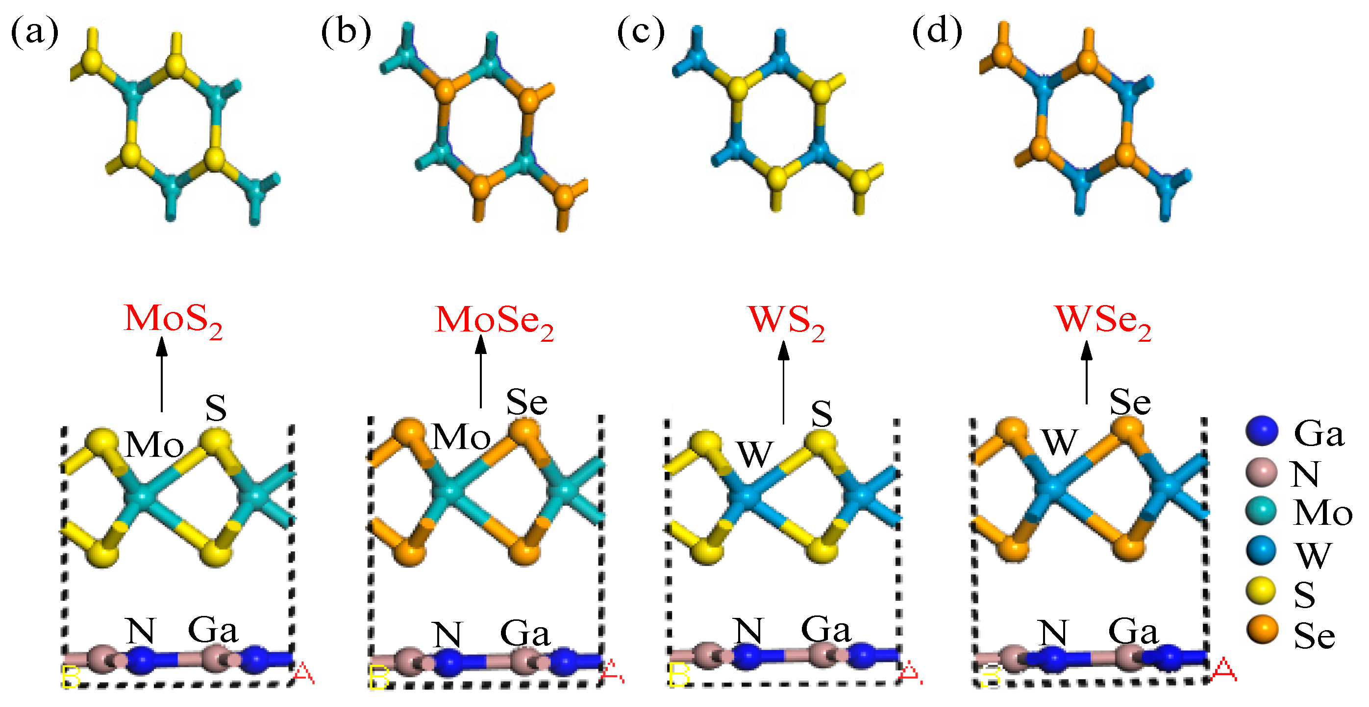
2.1. Geometric Parameters and System Stability

Geometric Parameters and Stability

The lattice parameters of GaN-MX2 are shown in Table 1. The lattice mismatch rate (σ) of the four heterostructures was calculated in this study to investigate their lattice matching, following Formula (1) [24].
σ = ( a 1 a 2 ) a 1 × 100 %
where a1 and a2 are the lattice constants of single-layer GaN and MX2 supercells, respectively. The calculated σ values for the four different heterojunctions are presented in Table 1, all of which remained below 3.5%, satisfying the conditions of complete coherence (|σ| < 5%).
Meanwhile, to investigate the stability of heterojunctions, we performed calculations on the binding energies (Eb) of GaN-MX2, where a more negative value indicates a higher degree of system stability. The mathematical expression for the Eb of heterojunctions can be formulated as follows [25]:
E b = E GaN - MX 2 M = M o , W ; X = S , S e E ( GaN ) E MX 2 M = M o , W ; X = S , S e
where E(GaN-MX2) denotes the energy of GaN-MX2, while E(GaN) and E(MX2) represent the energies of GaN and MX2, respectively. The calculated values of Eb are presented in Table 1. It is evident that all heterojunctions exhibited negative Eb values, indicating their inherent structural stability. Among the four systems, GaN-MoSe2 demonstrated the lowest binding energy, implying its superior structural stability.

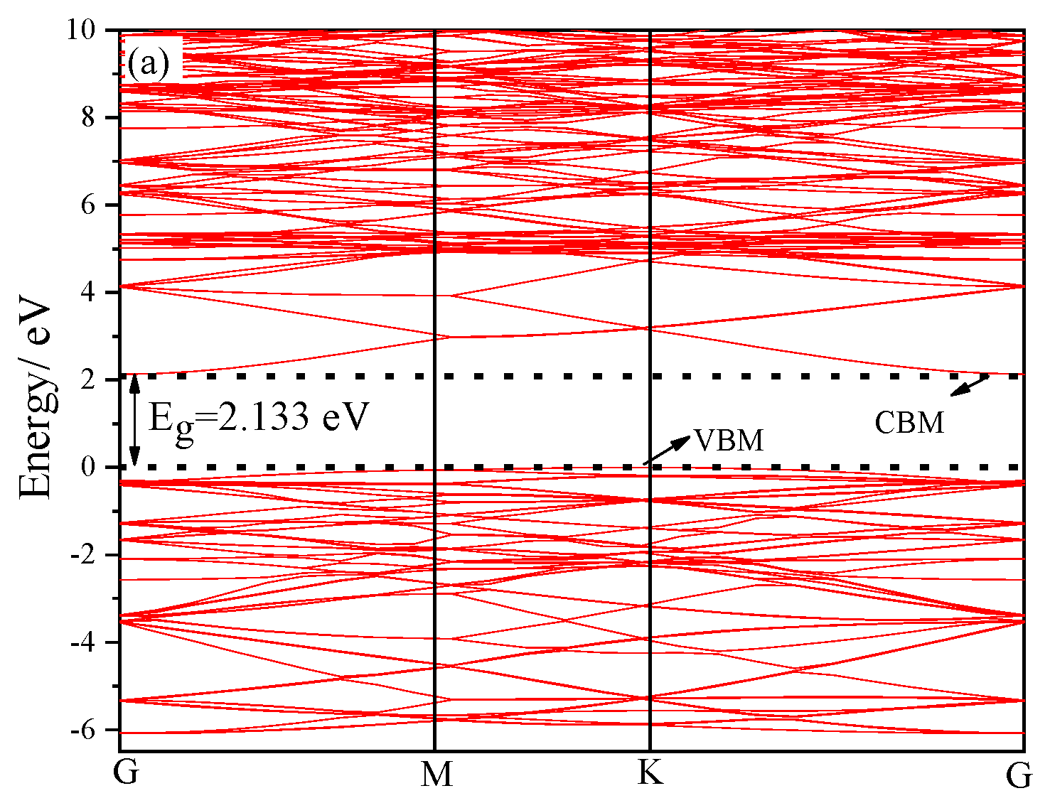
2.2. Electronic Structure Analysis

In order to facilitate the investigation of the electronic structure of GaN-MX2, we defined the Fermi level at 0 eV, as depicted in Figure 1. Figure 1a illustrates the band diagram of a monolayer GaN. The figure demonstrates that the conduction band minimum (CBM) of single-layer GaN is situated at the high symmetry point G, while the valence band maximum (VBM) is located at the high symmetry point K. This observation indicates an indirect band gap with a width of 2.133 eV for the system.
The energy band diagram of GaN-MoS2 is depicted in the left image of Figure 1b. It was observed that both the CBM and VBM were situated at the high symmetry point Q, indicating a direct band gap with a forbidden bandwidth of 0.856 eV for GaN-MoS2. Moreover, this material exhibited a downward shift toward lower energy levels, thereby reducing the energy required for electron transitions from the valence band to the conduction band. This is consistent with the results calculated by Tian et al. [26], which proves that the parameter selection in this study is reasonable. In conjunction with the density of states (DOS) plot presented in the left picture of Figure 1b, it was observed that GaN predominantly contributed to VBM, while MoS2 primarily contributed to CBM in GaN-MoS2, indicating distinct system-specific contributions to VBM and CBM. Consequently, GaN-MoS2 exhibiting this band characteristic was classified as a type II heterojunction.
The left panel in Figure 1c illustrates the band structure of GaN-MoSe2. Compared to single-layer GaN, the conduction band exhibited a downward shift in energy and a reduction in the band gap by 1.426 eV. The DOS plot for GaN-MoSe2 is depicted in the image on the right-hand side (Figure 1c). The analysis revealed that the VBM was primarily determined by contributions from GaN, while the CBM was predominantly influenced by MoSe2. Their combined effect led to a reduced bandwidth. This system exhibited a similar electric structure to GaN-MoS2 and was also classified as a type II heterojunction.
The band diagram of GaN-WS2 (left image) in Figure 1d exhibited a downward shift in energy, revealing a narrower bandgap, measured at 1.161 eV, compared to that of single-layer GaN. Additionally, it was observed that GaN-WS2 exhibited a distinct characteristic of having a direct bandgap. The DOS plot in Figure 1d (right image) reveals that the VBM was mainly contributed by GaN, while the CBM was primarily influenced by WS2. Therefore, this system can be classified as a type II heterojunction material.
The energy bands of GaN-WSe2 in Figure 1e (left image) transitioned from an indirect to a direct bandgap, resulting in a reduced width of 1.622 eV compared to single-layer GaN. This reduction effectively lowered the energy required for electron transition [27]. Furthermore, based on the DOS plot in Figure 1e (right image), it is evident that WSe2 significantly contributed to the CBM, while GaN dominated the VBM, confirming this system as a type II heterojunction material.

2.3. Work Function

The work function (Φ), as defined by Equation (5), quantifies the energy required to overcome the surface potential barrier, enabling electrons to escape from a solid surface (Fermi level, EF) and reach the vacuum energy level (Evac) [28]. This formula is as follows:
Φ = E vac E F
Therefore, we calculated the work functions for four GaN-MX2 systems and compared the results of this study with both the calculated and experimental values of other studies, as shown in Table 2. It was found that the calculated values in this study are very close to those obtained by others, indicating that the calculated results presented in this paper are reliable, as illustrated in Figure 2. In GaN-MoS2, the minimum work function of MoS2 exhibited an 11.06 eV reduction compared to that of GaN. Electrons were required to undergo transfer from MoS2, characterized by a lower potential, to GaN, characterized by a higher potential, until the same EF was reached. MoS2 accumulated positive charges on its surface, while GaN accumulated negative charges on its surface during the process. Consequently, a built-in electric field was present at the interface, oriented from GaN toward MoS2. This built-in field facilitated the efficient separation of electron–hole pairs, thereby significantly enhancing the photocatalytic activity of the system.
Through extrapolation, the other three heterojunctions exhibited varying potential differences at the interface, indicating the generation of distinct built-in electric fields. Notably, the interface potential differences of GaN-MoS2 and GaN-MoSe2 were significantly larger than those of the other two heterojunctions. Although GaN-MoSe2 demonstrated a slightly smaller potential difference compared to GaN-MoS2, this disparity was not statistically significant. Consequently, it can be inferred that among these four heterojunctions, GaN-MoS2 exhibited superior electron–hole separation ability, followed by GaN-MoSe2. Based on this observation, it can be speculated that both GaN-MoS2 and GaN-MoSe2 possess commendable photocatalytic capabilities.

2.4. Optical Properties

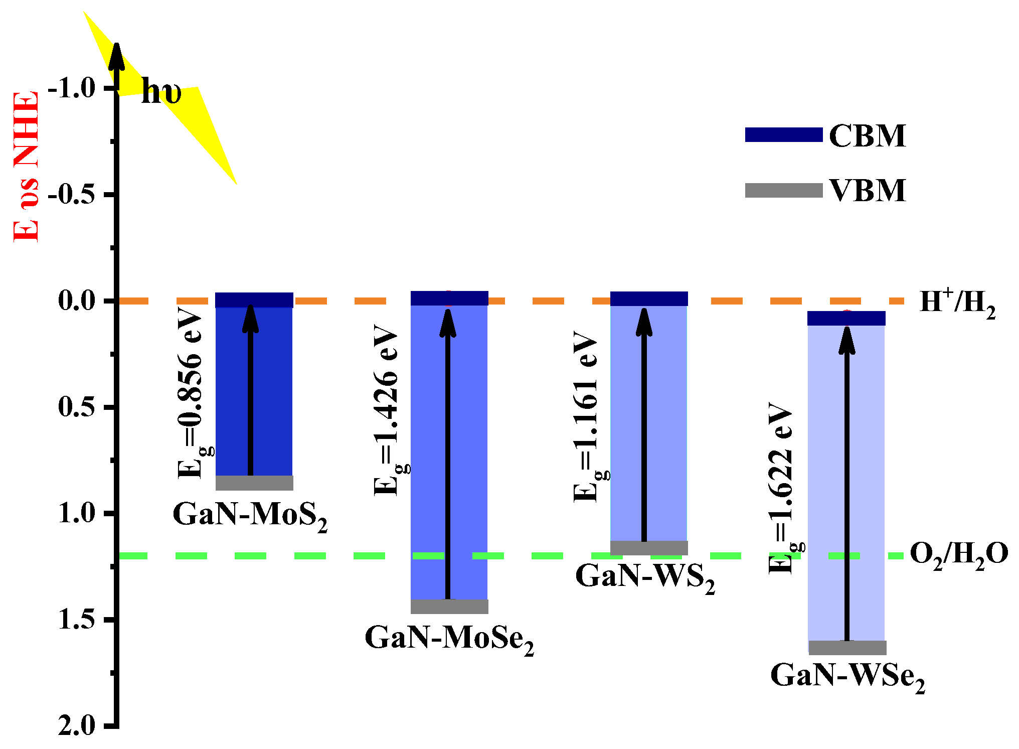
2.4.1. Alignment with Band Structure Edges

Typically, photocatalysts are evaluated based on the relative positions of their semiconductor conduction band max (CBM) and valence band min (VBM) values with respect to the standard hydrogen electrode (NHE). Determining the band-edge potential on the NHE scale commonly relies on Equations (4) and (5) [32]. In the two equations, X represents the absolute electronegativity of the material. The energy level of free electrons on the NHE scale, which is approximately 4.5 eV, is denoted as Eelce. On the contrary, Eg refers to the band gap of a semiconductor.
E CBM = X E elec 0.5 E g
E VBM = VBM + E g
The band-edge potential on the NHE scale of the four heterojunctions is depicted in Figure 3, revealing that the CBMs of GaN-MoS2 and GaN-WS2 lie above the H+/H2 potential, indicating their capability to evolve hydrogen. However, the VBMs of both systems did not fall below the O2/H2O potential, suggesting their inability to evolve oxygen. Conversely, GaN-WSe2 solely possessed the ability to evolve oxygen, while only GaN-MoSe2 exhibited simultaneous hydrogen and oxygen evolution capabilities. Consequently, it can be inferred that, among these four heterojunctions, GaN-MoSe2 has superior photocatalytic activity for water splitting.

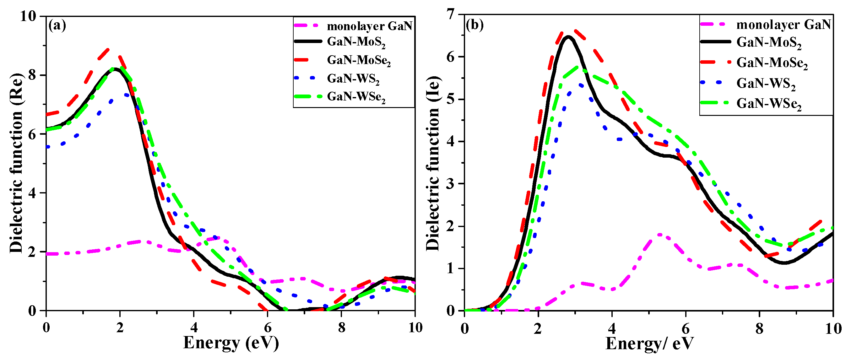
2.4.2. Dielectric Function

The variation in the real and imaginary parts of the dielectric function for GaN-MX2 with incident photon energy is depicted in Figure 4. In Figure 4a, the real part of the dielectric function for GaN-MX2 is presented. The stronger the static dielectric constant, the greater the binding ability and polarization capability toward charges in the system. This figure reveals that the static dielectric constants for monolayer GaN and GaN-MX2 systems were 1.938, 6.195, 6.663, 5.574, and 6.153, respectively, satisfying the equation ε ( 0 ) 1 + ( ω E g ) 2 [14]. The GaN-MX2 system exhibited a higher static dielectric constant compared to that of single-layer GaN, suggesting enhanced charge confinement and polarization capabilities in the GaN-MX2 heterojunctions. Among these systems, GaN-MoSe2 demonstrated the highest static dielectric constant, indicating faster migration of photogenerated carriers within the crystal, thus enhancing its photocatalytic activity. The imaginary part of the dielectric function for GaN-MX2 is depicted in Figure 4b. As the value increased, the likelihood of electron absorption of photons in the system also increased, resulting in a higher population of electrons in an excited state. From the graph, it is evident that single-layer GaN, GaN-WS2, GaN-WSe2, GaN-MoS2, and GaN-MoSe2 manifested their first noticeable peak within the visible light range at energy levels of 3.146, 2.827, 2.798, 3.137, and 2.991 eV, respectively. This observation highlights a redshift phenomenon in the GaN-MX2 systems, which may have significant implications for future research in this field. Among them, GaN-MoSe2 presented the highest imaginary part of the dielectric function value, indicating a greater propensity for electron absorption of photons and consequently possessing a higher population of excited electrons. Therefore, it can be inferred that this system has superior photocatalytic performance.
In summary, compared to monolayer GaN, GaN-MX2 exhibited an increased static dielectric constant and a redshift phenomenon, indicating an enhanced polarization ability and binding energy. Consequently, there is a higher likelihood of electron absorption of photons and an increase in excited state electrons. Therefore, the probability of electron transition is also amplified. Thus, constructing heterojunctions serves as a means to enhance the photocatalytic performance of the system.

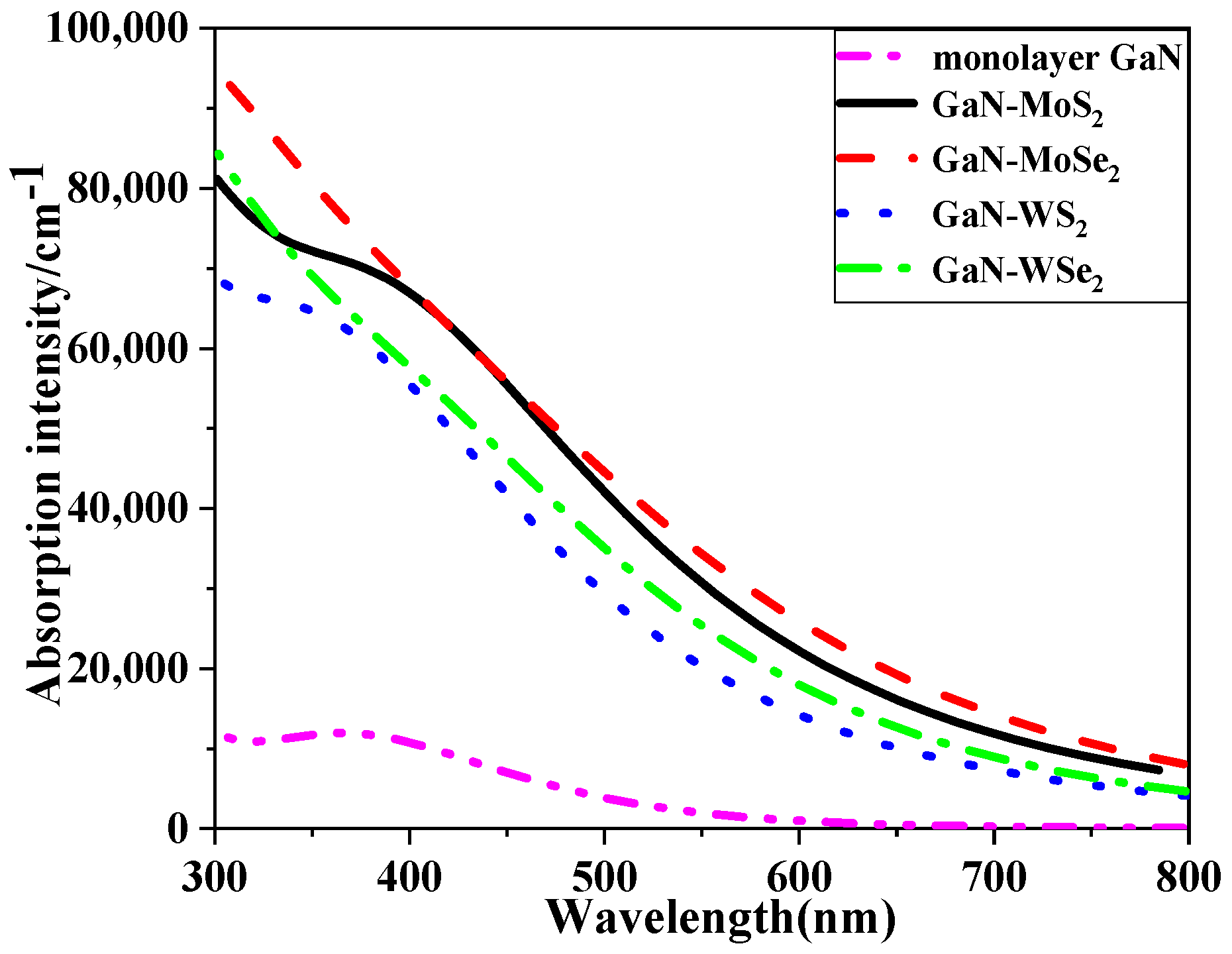
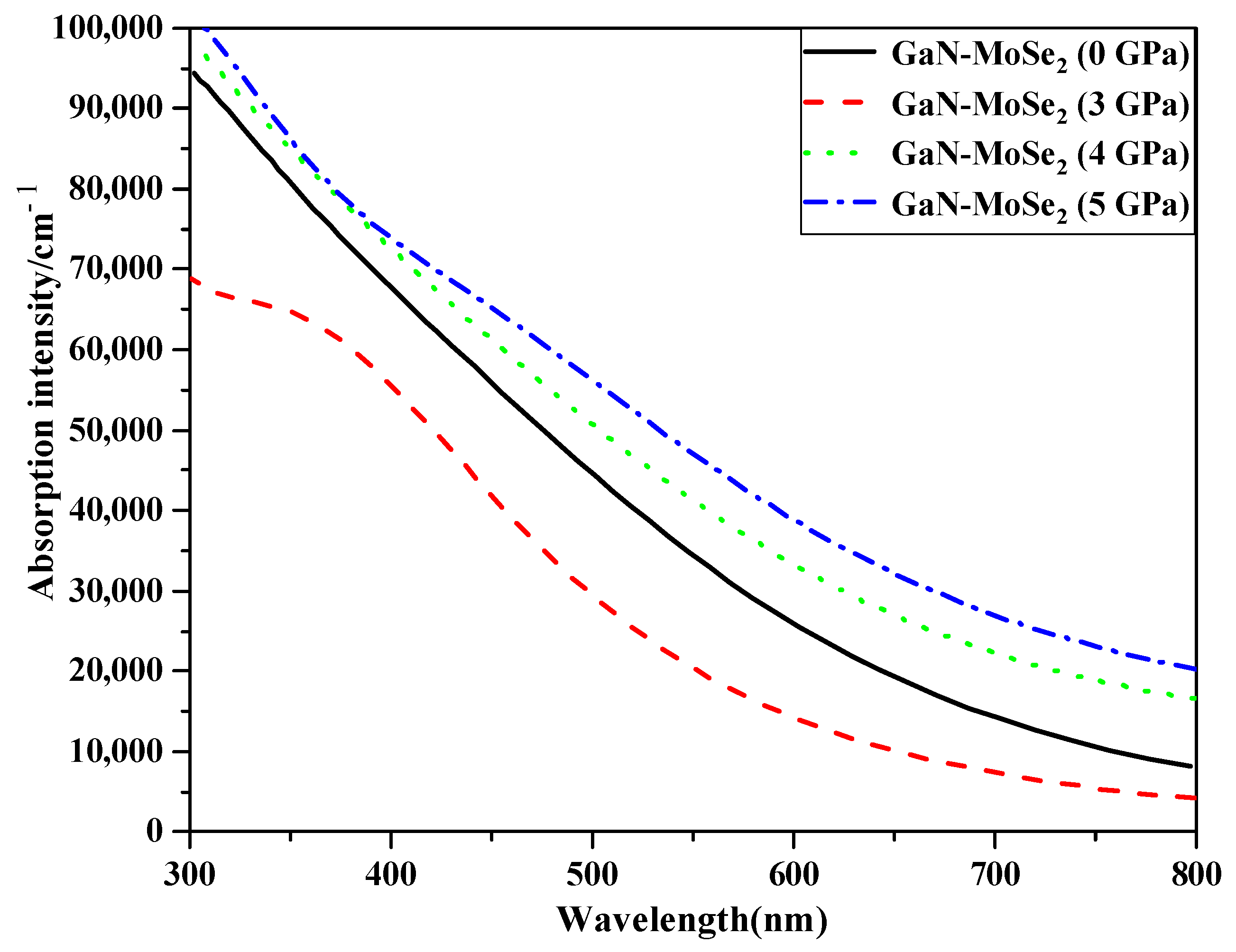
2.4.3. Absorption Spectra

The absorption spectra of GaN-MX2 as a function of incident wavelength are depicted in Figure 5. It can be observed from the graph that within the visible light range, all four systems of GaN-MX2 exhibited significantly higher absorption intensity compared to monolayer GaN. The constructed GaN-MX2 heterojunctions exhibited superior photocatalytic activity compared to monolayer GaN. Among these systems, it is noteworthy that GaN-MoSe2 demonstrated the highest absorption intensity due to enhanced interaction between the 4d state of Mo and the 4p state of Se, as well as between the 4p state of Ga and the 2p state of N in this particular heterojunction. Consequently, there was an increased number of electron transitions, which beneficially impacted the photocatalytic efficiency of GaN-MoSe2. Importantly, this result aligns with analysis based on dielectric functions [5].

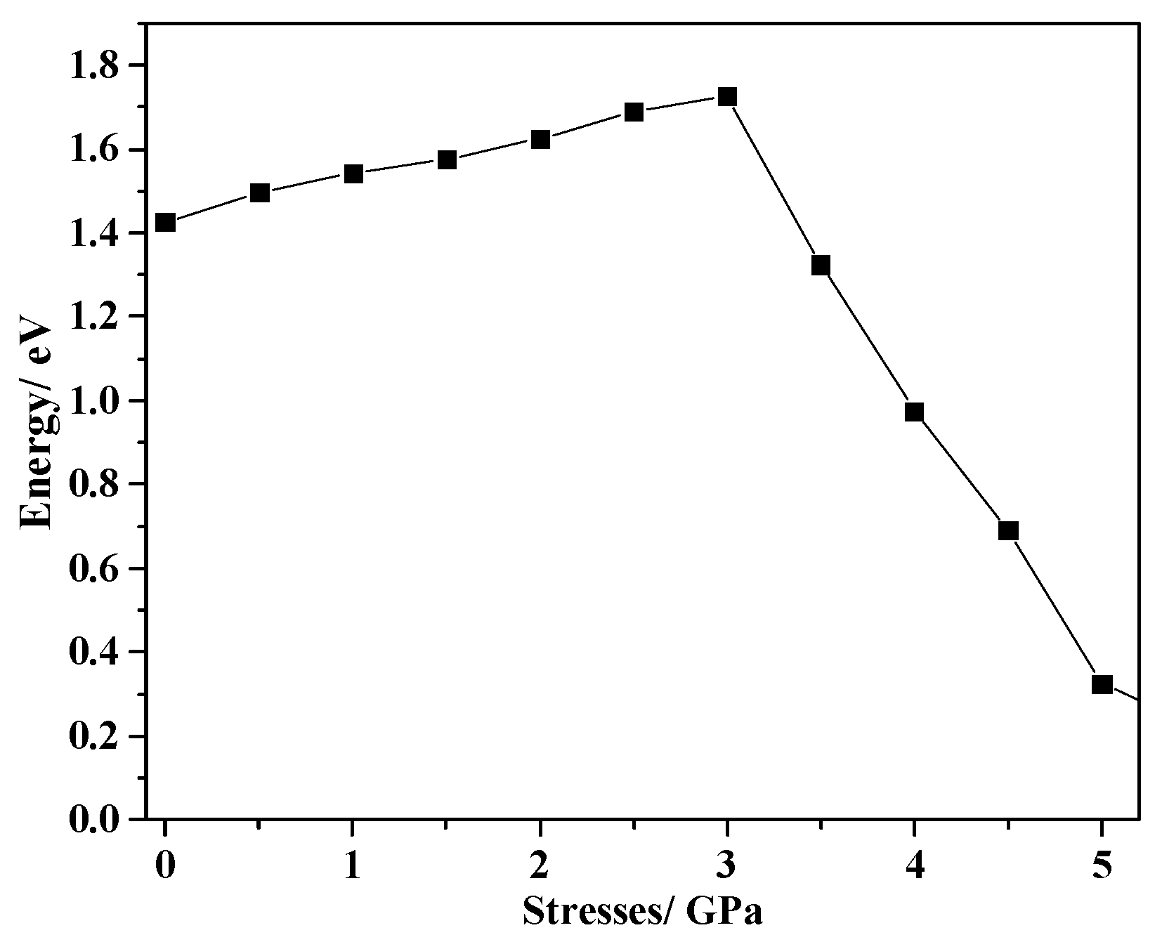
2.5. Applying Pressure

Based on the aforementioned analysis, it is evident that GaN-MoSe2 exhibited a commendable photocatalytic performance. In general, applying stress engineering to a photocatalyst can further enhance its photocatalytic capability. Consequently, GaN-MoSe2, with superior photocatalytic performance, was chosen for subsequent implementation of stress engineering regulations. As illustrated in Figure 6, variations in Eg of GaN-MoSe2 were observed under stress levels ranging from 3 to 6 GPa. The effect of stress on the electronic structure of GaN-MoSe2 was highly significant, as evidenced by the observed increase in Eg followed by a gradual decrease with increasing pressure. The aforementioned observation suggests that stress exerts a robust influence on the catalytic activity of GaN-MoSe2, as convincingly demonstrated by the light absorption spectra (Figure 7) obtained under various stress conditions. The results depicted in Figure 7 indicate that the light absorption capacity of GaN-MoSe2 was enhanced under pressures of 3 and 6 GPa, compared to GaN-MoSe2 without pressure. Therefore, the implementation of stress engineering can further enhance the photocatalytic activity of GaN-MoSe2, which exhibited superior photocatalytic performance compared to the other three heterojunctions.

3. Computational Methods and Theoretical Model

The selected GaN structure in this study was wurtzite, belonging to the P63mc (No. 186) space group, with lattice constants of a = b = 0.318 nm and c = 0.517 nm and angles of α = β = 90° and γ = 120° [33]. The transition metal chalcogenide MX2 exhibited the 2H phase [34]. First, geometric optimization of both GaN and MX2 unit cells was performed individually. Subsequently, they were cleaved along the (001) direction to fabricate heterostructures. Additionally, a vacuum layer with a thickness of 18 Å was incorporated along the c-axis to mitigate interlayer coupling effects. Based on the convergence test diagram (Figure 8), the supercell size of GaN-MX2 was set to 2 × 2 × 1, ensuring calculation accuracy while conserving computing resources. Therefore, we constructed GaN-MX2 models using a 2 × 2 × 1 supercell while ensuring computational accuracy, as illustrated in Figure 9. The valence electron configurations for the six atoms involved in this study were as follows: Ga (4s24p1), N (2s22p3), Mo (4d55s1), W (5d46s2), S (3s23p4), and Se (4s24p4).
The calculation in this article was based on density functional theory (DFT), utilizing the CASTEP module within the Materials Studio software package (version 2017). The plane wave super soft pseudo potential was employed to describe the interaction between valence electrons and ions, while the generalized gradient approximation GGA-PBE was utilized for exchange–correlation energy during geometry optimization [35]. Considering the limitations of DFT in accurately describing van der Waals (vdW) interactions, the incorporation of Tkatchenko–Scheffler (TS) dispersion correction is essential during the calculation process [31]. The plane wave cutoff energy was set to 550 eV. The K-point grid was set as 5 × 5 × 1 under the Monkhorst–Pack scheme [36]. The BFGS algorithm was employed, incorporating a self-consistent field (SCF) convergence criterion of 2.0 × 10⁻⁶ eV/atom and a maximum interatomic stress limit of 0.1 GPa. All calculations were conducted within the reciprocal lattice space [37].

4. Conclusions

The structural stability, electronic structure, and optical properties of GaN-MX2 (M=Mo, W; X=S, Se) heterojunctions were investigated in this study using the CASTEP module. Through first principle calculations, it was shown that GaN-MX2 exhibited low lattice mismatches (<3.5%), thereby ensuring lattice coherence. Notably, GaN-MoSe2 demonstrated the lowest binding energy, indicating its high stability. The four heterojunctions exhibited a smaller direct band gap compared to single-layer GaN, which had an indirect band gap. All heterojunctions were of type II. Calculation of the work functions revealed that GaN-MoS2 and GaN-MoSe2 have relatively larger interface potential differences, indicating stronger built-in electric fields and, thus, the strongest electron–hole separation ability. Among the four heterojunctions, GaN-MoSe2 exhibited the highest real part value of the dielectric function, indicating its superior electronic polarization ability under an electric field and, consequently, the highest electron mobility, as well as the most pronounced optical absorption capacity. Therefore, it can be inferred that GaN-MoSe2 possesses the strongest photocatalytic capability. The primary distinction between this investigation and prior ones lies in the computation of the band structure and optical properties of GaN-MoSe2 under applied pressure. The findings demonstrate that the application of stress significantly impacted the band gap width and light absorption capacity of GaN-MoSe2. Specifically, when subjected to a pressure of 5 GPa, it demonstrated a significantly narrower band gap and heightened absorption capacity in comparison to its intrinsic state. These results suggest that the application of stress has the potential to further enhance its photocatalytic performance. Future studies could explore the application of biaxial strain on GaN-MoSe2 to observe changes in its electronic structure and optical properties so as to speculate on the modulation effect of its photocatalytic capacity.

Author Contributions

Conceptualization, X.-C.Z., L.-L.Z., and H.-M.L.; data curation, X.-C.Z., C.Z., and Q.-Y.C.; formal analysis, X.-C.Z.; funding acquisition, X.-C.Z.; investigation, X.-C.Z., M.-Y.D., and F.-M.L.; methodology, X.-C.Z., Y.-N.H., and H.-M.L.; project administration, L.-L.Z.; validation, X.-C.Z., H.-M.L., and X.-C.Q.; visualization, X.-C.Z., M.-Y.D., and F.-M.L.; writing—original draft, X.-C.Z., M.-Y.D., and F.-M.L.; writing—review and editing, L.-L.Z., Y.-N.H., and H.-M.L. All authors have read and agreed to the published version of the manuscript.

Funding

This study was supported by the Science and Technology Program of Xinjiang Yili Kazakh Autonomous Prefecture (No. YJC2023A02), the Scientific Research Project of Yili Normal University (No. 2024YSZD010), and the Innovative Training Program of Undergraduates of Yili Normal University (No. S202310764006).

Institutional Review Board Statement

Not applicable.

Informed Consent Statement

Not applicable.

Data Availability Statement

The original contributions presented in this study are included in the article; further inquiries can be directed to the corresponding authors.

Conflicts of Interest

The authors declare no conflicts of interest.

References

  1. Li, Y.R.; Li, S.T.; Huang, H.W. Metal-enhanced strategies for photocatalytic and photoelectrochemical CO2 reduction. Chem. Eng. J. 2023, 457, 141179. [Google Scholar] [CrossRef]
  2. Hu, Y.F.; Li, B.L.; Yu, C.L.; Fang, H.C.; Li, Z.S. Mechanochemical preparation of single atom catalysts for versatile catalytic applications: A perspective review. Mater. Today 2023, 63, 288–312. [Google Scholar] [CrossRef]
  3. Zhang, Y.; Qi, M.Y.; Tang, Z.R.; Xu, Y.J. Photoredox-catalyzed plastic waste conversion: Nonselective degradation versus selective synthesis. ACS Catal. 2023, 13, 3575–3590. [Google Scholar] [CrossRef]
  4. Tan, D.M.; Zhuang, R.; Chen, R.C.; Ban, M.H.; Feng, W.; Xu, F.; Chen, X.; Wang, Q.Y. Covalent organic frameworks enable sustainable solar to hydrogen peroxide. Adv. Funct. Mater. 2024, 34, 2311655. [Google Scholar] [CrossRef]
  5. Wu, Z.X.; Yang, P.F.; Li, Q.C.; Xiao, W.P.; Li, Z.J.; Xu, G.R.; Liu, F.S.; Jia, B.H.; Ma, T.Y.; Feng, S.H.; et al. Microwave synthesis of pt clusters on black TiO2 with abundant oxygen vacancies for efficient acidic electrocatalytic hydrogen evolution. Angew. Chem. Int. Ed. Engl. 2023, 62, e202300406. [Google Scholar] [CrossRef]
  6. Yan, S.C.; Li, Z.S.; Zou, Z.G. Photodegradation performance of g-c3n4 fabricated by directly heating melamine. Langmuir ACS J. Surf. Colloids 2009, 25, 10397–10401. [Google Scholar] [CrossRef]
  7. Bera, R.; Kundu, S.; Patra, A. 2d hybrid nanostructure of reduced graphene oxide-CdS nanosheet for enhanced photocatalysis. ACS Appl. Mater. Interfaces 2015, 7, 13251–13259. [Google Scholar] [CrossRef]
  8. Jung, H.S.; Hong, Y.J.; Li, Y.; Cho, J.; Kim, Y.; Yi, G. Photocatalysis using GaN nanowires. ACS Nano 2008, 2, 637–642. [Google Scholar] [CrossRef]
  9. Watanabe, K.; Taniguchi, T.; Kanda, H. Direct-bandgap properties and evidence for ultraviolet lasing of hexagonal boron nitride single crystal. Nat. Mater. 2004, 3, 404–409. [Google Scholar] [CrossRef]
  10. Winnerl, J.; Kraut, M.; Artmeier, S.; Stutzmann, M. Selectively grown GaN nanowalls and nanogrids for photocatalysis: Growth and optical properties. Nanoscale 2019, 11, 4578–4584. [Google Scholar] [CrossRef]
  11. Tagliabue, G.; Duchene, J.S.; Abdellah, M.; Habib, A.; Gosztola, D.J.; Hattori, Y.; Cheng, W.; Zheng, K.; Canton, S.E.; Sundararaman, R.; et al. Ultrafast hot-hole injection modifies hot-electron dynamics in au/p-GaN heterostructures. Nat. Mater. 2020, 19, 1312–1318. [Google Scholar] [CrossRef] [PubMed]
  12. Zhang, W.D.; Brown, E.R.; Growden, T.A.; Berger, P.R. Investigation of peak-to-valley current ratio of GaN/AlN resonant tunneling diodes. IEEE Trans. Electron Devices 2023, 70, 3483–3488. [Google Scholar] [CrossRef]
  13. Fu, S.; Xiao, Q.; Yao, Y.; Zou, M.; Tang, H.; Ye, J.; Xie, Q. First principles study of the effect of nitrogen defects on the electronic structure and optical property of GaN/g-c3n4 heterojunction. Chin. J. Inorg. Chem. 2023, 39, 1721–1728. [Google Scholar] [CrossRef]
  14. Han, W.; Liu, Z.; Yu, H. Synthesis and optical properties of GaN/ZnO solid solution nanocrystals. Appl. Phys. Lett. 2010, 96, 183112. [Google Scholar] [CrossRef]
  15. Jena, K.; Swain, R.; Lenka, T.R. Impact of a drain field plate on the breakdown characteristics of AlInN/GaN MOSHEMT. J. Korean Phys. Soc. 2015, 67, 1592–1596. [Google Scholar] [CrossRef]
  16. Mohanta, M.K.; Sarkar, A.D. Tweaking the physics of interfaces between monolayers of buckled cadmium sulfide for a superhigh piezoelectricity, excitonic solar cell efficiency, and thermoelectricity. ACS Appl. Mater. Interfaces 2020, 12, 18123–18137. [Google Scholar] [CrossRef]
  17. Rasool, A.; Anis, I.; Bhat, S.A.; Dar, M.A. Optimizing the NRR activity of single and double boron atom catalysts using a suitable support: A first principles investigation. Phys. Chem. Chem. Phys. 2023, 25, 22275–22285. [Google Scholar] [CrossRef]
  18. Li, J.; Chen, L.; Hua, Z.; Liu, B. Enhanced photoelectrochemical performance of cobalt phosphate modified GaN-ZnO nanowires/GaN microrods heterostructure photoanode by vacancy defect modulation. Appl. Surf. Sci. 2024, 642, 158607. [Google Scholar] [CrossRef]
  19. Li, Y.; Li, Q.; Zhang, C.; Pu, H.; Zhang, Y.; Zhang, J.; Hao, Y. Transport properties of InGaN channel-based heterostructures with GaN interlayers. J. Electron. Mater. 2024, 53, 1105–1115. [Google Scholar] [CrossRef]
  20. Guan-Shi, W.; Yan-Ming, L.; Ya-Li, Z.; Zhen-Yi, J.; Xiao-Doug, Z. Electronic and optical performances of (Cu, N) codoped TiO2/MoS2 heterostructure photocatalyst: Hybrid DFT (HSE06) study. Acta Phys. Sin. 2018, 67, 233101. [Google Scholar] [CrossRef]
  21. Guo, W.; Luo, H.; Jiang, Z.; Shangguan, W. In-situ pressure-induced BiVO4/bi0. 6y0. 4VO4 s-scheme heterojunction for enhanced photocatalytic overall water splitting activity. Chin. J. Catal. 2022, 43, 316–328. [Google Scholar] [CrossRef]
  22. Ma, Q.F.; Ma, J.Y.; Sun, X.F.; Chen, X.J.; Liu, G.R.; Yang, H. Theoretical and experimental elucidation of synergistic enhanced piezo-photocatalysis and mechanism of BiVO4 for organic pollutant degradation. Mater. Res. Bull. 2024, 170, 112559. [Google Scholar] [CrossRef]
  23. Qiu, G.; Xiao, Q.; Hu, Y.; Qin, W.; Wang, D. Theoretical study of the surface energy and electronic structure of pyrite FeS2 (100) using a total-energy pseudopotential method, CASTEP. J. Colloid. Interface. Sci. 2004, 270, 127–132. [Google Scholar] [CrossRef] [PubMed]
  24. Zheng, J.; Zhao, Q.; Tang, T.; Yin, J.; Quilty, C.D.; Renderos, G.D.; Liu, X.; Deng, Y.; Wang, L.; Bock, D.C.; et al. Reversible epitaxial electrodeposition of metals in battery anodes. Science 2019, 366, 645–648. [Google Scholar] [CrossRef]
  25. Kresse; Furthmuller Efficient iterative schemes for ab initio total-energy calculations using a plane-wave basis set. Phys. Review. B Condens. Matter 1996, 54, 11169–11186. [CrossRef]
  26. Tian, F.; Kong, D.L.; Qiu, P.; Liu, H.; Zhu, X.L.; Wei, H.Y.; Song, Y.M.; Chen, H.; Zheng, X.H.; Peng, M.Z. Polarization modulation on charge transfer and band structures of GaN/MoS2 polar heterojunctions. Crystals 2023, 13, 563. [Google Scholar] [CrossRef]
  27. Khanam, R.; Hassan, A.; Nazir, Z.; Dar, M.A. Nickel single atom catalyst supported on the gallium nitride monolayer: First principles investigations on the decisive role of support in the electrocatalytic reduction of CO2. Sustain. Energ. Fuels 2023, 7, 5046–5056. [Google Scholar] [CrossRef]
  28. Zhang, X.; Matras-Postolek, K.; Yang, P.; Jiang, S.P. Z-scheme WOx/cu-g-c3n4 heterojunction nanoarchitectonics with promoted charge separation and transfer towards efficient full solar- spectrum photocatalysis. J. Colloid. Interface. Sci. 2023, 636, 646–656. [Google Scholar] [CrossRef] [PubMed]
  29. Ma, L.; Li, M.N.; Zhang, L.L. Electronic and optical properties of GaN/MoSe2 and its vacancy heterojunctions studied by first-principles. J. Appl. Phys. 2023, 133, 045307. [Google Scholar] [CrossRef]
  30. Goodarzi, N.; Ashrafi-Peyman, Z.; Khani, E.; Moshfegh, A.Z. Recent progress on semiconductor heterogeneous photocatalysts in clean energy production and environmental remediation. Catalysts 2023, 13, 1102. [Google Scholar] [CrossRef]
  31. Hermann, J.; Distasio, R.A.J.; Tkatchenko, A. First-principles models for van der waals interactions in molecules and materials: Concepts, theory, and applications. Chem. Rev. 2017, 117, 4714–4758. [Google Scholar] [CrossRef] [PubMed]
  32. Wang, X.M.; Yan, Y.F. Optical activity of solids from first principles. Phys. Rev. B 2023, 107, 045201. [Google Scholar] [CrossRef]
  33. Barnett, R.L.; Polkovnikov, A.; Demler, E.; Yin, W.; Ku, W. Coexistence of gapless excitations and commensurate charge-density wave in the 2h transition metal dichalcogenides. Phys. Rev. Lett. 2006, 96, 26406. [Google Scholar] [CrossRef] [PubMed]
  34. Choudhary, K.; Tavazza, F. Convergence and machine learning predictions of monkhorst-pack k-points and plane-wave cut-off in high-throughput DFT calculations. Comput. Mater. Sci. 2019, 161, 300–308. [Google Scholar] [CrossRef]
  35. Faccio, R.; Denis, P.A.; Pardo, H.; Goyenola, C.; Mombru, A.W. Mechanical properties of graphene nanoribbons. J. Phys. Condens. Matter Inst. Phys. J. 2009, 21, 285304. [Google Scholar] [CrossRef]
  36. Armakovic, S.J.; Savanovic, M.M.; Armakovic, S. Titanium dioxide as the most used photocatalyst for water purification: An overview. Catalysts 2023, 13, 26. [Google Scholar] [CrossRef]
  37. Pavel, M.; Anastasescu, C.; State, R.N.; Vasile, A.; Papa, F.; Balint, I. Photocatalytic degradation of organic and inorganic pollutants to harmless end products: Assessment of practical application potential for water and air cleaning. Catalysts 2023, 13, 380. [Google Scholar] [CrossRef]
Figure 1. The band structure and DOS diagrams for single-layer GaN and GaN-MX2: (a) monolayer GaN; (b) GaN-MoS2; (c) GaN-MoSe2; (d) GaN-WS2; (e) GaN-WSe2.
Catalysts 14 00732 g001aCatalysts 14 00732 g001b
Figure 2. Work function diagram of GaN-MX2.
Catalysts 14 00732 g002
Figure 3. Band-edge potential maps for single-layer GaN and GaN-MoS2, GaN-MoSe2, GaN-WS2, and GaN-WSe2.
Catalysts 14 00732 g003
Figure 4. Plots of the dielectric functions for GaN-MX2: (a) the real part of the dielectric function plot; (b) the imaginary part of the dielectric function plot.
Catalysts 14 00732 g004
Figure 5. The absorption spectra of GaN-MX2.
Catalysts 14 00732 g005
Figure 6. Variation in GaN-MoSe2 Eg as a function of applied stress.
Catalysts 14 00732 g006
Figure 7. Stress-induced light absorption spectra of GaN-MoSe2.
Catalysts 14 00732 g007
Figure 8. Convergence test for supercell geometry optimization.
Catalysts 14 00732 g008
Figure 9. Top and side views of the 2 × 2 × 1 supercell models of GaN-MX2: (a) GaN-MoS2, (b) GaN-MoSe2, (c) GaN-WS2, and (d) GaN-WSe2. The capital letters “A” and “B” denote the “A” axis and “B” axis of the unit cell model, respectively.
Catalysts 14 00732 g009
Table 1. Lattice constants of GaN-MX2 after optimization.
Model GaN-MoS2 GaN-MoSe2 GaN-WS2 GaN-WSe2
σ /% 0.5 3.3 0.1 3.2
Eb/eV −0.1385 −0.1512 −0.1347 −0.1498
Cell volume/Å3 786.404 826.206 825.014 846.888
Length (Å) 2.9505 2.5270 2.4218 2.4838
Table 2. Summary of the work functions of GaN-MoS2, GaN-MoSe2, GaN-WS2, and GaN-WSe2.
GaN-MoS2GaN-MoSe2GaN-WS2GaN-WSe2
Φ (this work)5.042 eV5.077 eV4.699 eV4.735 eV
Φ (calculated values)5.17 eV [26]5.091 eV [29]4.57 eV [30]4.92 eV [31]
Φ (experimental values)5.26 eV [26]---
Disclaimer/Publisher’s Note: The statements, opinions and data contained in all publications are solely those of the individual author(s) and contributor(s) and not of MDPI and/or the editor(s). MDPI and/or the editor(s) disclaim responsibility for any injury to people or property resulting from any ideas, methods, instructions or products referred to in the content.

