Review

Photoactive Heterostructures: How They Are Made and Explored

by
Alexei V. Emeline
1,
Aida V. Rudakova
1,
Ruslan V. Mikhaylov
1,
Kirill M. Bulanin
1,2 and
Detlef W. Bahnemann
1,3,*
1
Laboratory “Photoactive Nanocomposite Materials”, Saint-Petersburg State University, Ulianovskaia 1, Peterhof, 198504 Saint-Petersburg, Russia
2
Institute of Quantum Physics, Irkutsk National Research Technical University, Lermontov St. 83, 664074 Irkutsk, Russia
3
Institut fuer Technische Chemie, Gottfried Wilhelm Leibniz Universität Hannover, Callinstrasse 3, D-30167 Hannover, Germany
*
Author to whom correspondence should be addressed.
Catalysts 2021, 11(2), 294; https://doi.org/10.3390/catal11020294
Submission received: 6 January 2021 / Revised: 5 February 2021 / Accepted: 9 February 2021 / Published: 23 February 2021
(This article belongs to the Special Issue Photocatalytic Nanocomposite Materials)

Abstract

:

Simple Summary

In our review we consider the results on the development and exploration of heterostructured photoactive materials with a major attention focused at what are the better ways to form this type of materials and how to explore them correctly. Regardless what type of heterostructure is formed, its functionality strongly depends on the quality of heterojunction. In turn, it depends on the selection of heterostructure components (their chemical and physical properties) and on the proper choice of the synthesis method. Several examples of the different approaches such as in-situ and ex-situ, bottom-up and top-down, are reviewed. At the same time, strong experimental physical evidences demonstrating true heterojunction formation are required. A possibility to obtain such evidences using different physical techniques is discussed.

Abstract

In our review we consider the results on the development and exploration of heterostructured photoactive materials with major attention focused on what are the better ways to form this type of materials and how to explore them correctly. Regardless of what type of heterostructure, metal–semiconductor or semiconductor–semiconductor, is formed, its functionality strongly depends on the quality of heterojunction. In turn, it depends on the selection of the heterostructure components (their chemical and physical properties) and on the proper choice of the synthesis method. Several examples of the different approaches such as in situ and ex situ, bottom-up and top-down, are reviewed. At the same time, even if the synthesis of heterostructured photoactive materials seems to be successful, strong experimental physical evidence demonstrating true heterojunction formation are required. A possibility for obtaining such evidence using different physical techniques is discussed. Particularly, it is demonstrated that the ability of optical spectroscopy to study heterostructured materials is in fact very limited. At the same time, such experimental techniques as high-resolution transmission electron microscopy (HRTEM) and electrophysical methods (work function measurements and impedance spectroscopy) present a true signature of heterojunction formation. Therefore, whatever the purpose of heterostructure formation and studies is, the application of HRTEM and electrophysical methods is necessary to confirm that formation of the heterojunction was successful.

1. Introduction

For decades heterogeneous photocatalysis and photoelectrochemistry have attracted significant attention from researchers working in the areas of both fundamental and applied science [1,2,3,4,5,6]. In recent years two major targets have been the focus of practical research: the activity and spectral sensitivity of photoactive materials. Several major approaches have been developed to achieve these targets, such as the creation of new photoactive materials, the physical and chemical modification of the known materials to improve their functional properties, and the formation of heterostructures on the basis of known and new materials to create a desired spectral and charge transfer response in the systems [7,8,9,10,11,12,13,14,15,16,17,18]. In recent years significant progress in the development of photoactive materials has been demonstrated in studies devoted to the design, characterization, exploration and application of various heterostructured materials [19,20,21,22,23,24]. In our review we consider the results of the development and exploration of heterostructured photoactive materials, with major attention focused on which are the better ways to form these materials and how to explore them correctly.
Here we denote a heterostructured photoactive material as an object possessing at least one heterojunction between two different components. In typical cases of polycrystalline photoactive materials, such solids as metals, semiconductors and dielectrics can be considered as components of heterostructures. At least one of the components must be a semiconductor (or dielectric) that provides a condition for sufficiently long life-time for the excited state of the heterostructure which is necessary to initiate a further chemical sequence. The AB heterostructures can be classified based on the configuration and dimensions of the interface between two components, A and B, as follows (see Figure 1): one-dimensional (1D), two-dimensional (2D) and three-dimensional (3D) heterostructures [25,26,27,28,29,30,31].
In a one-dimensional heterostructure, the interface is of line-like shape, that is, the contact area is extended in one direction and not expanded in two others. In this case, the particles (agglomerate of particles) of the same type forming the 1D structure, are separated from each other by another component in heterostructure. Typically, such heterostructured materials are formed with inclusions of nanowires, nanorods, nanotubes, nanofibers, etc. (Figure 1a).
Two-dimensional heterostructures have a plane-like interface between the particles of the components A and B. The dimension of the 2D heterojunction is more extended than the particle sizes of the one or both heterostructure components, and particles of the same type(s) form the layer(s) (Figure 1b). This is typical for planar heterostructures such as “layer-by-layer” systems. A distinguishing feature of the planar heterostructure is that the outer layer of the first component of heterostructure completely covers an inner layer of another component of heterostructure, which means that only the component forming the outer layer contacts with environmental media. This particular case is a formation of photoelectrochemical electrodes when photoactive a semiconductor layer is formed on conductive metal or semiconductor substrates (see Figure 1b, right image). Another possible structure of 2D heterostructure is a so called deposited heterostructure. In this case, both the substrate and the deposited components are in contact with the environment.
The interface of three-dimensional heterostructures extends in all three directions and can be described as a 3D surface of rather complex shape (Figure 1c). This type of heterostructured material is the most common and typically includes powdered (nanoparticle based) components. An illustrative example of a three-dimensional heterosystem is a core-shell structure. However, more typically, particles of such composite materials are the agglomerates of nano- or microcrystallites in contact with each other in different components of heterostructures. In more complex scenarios, 1D and 2D heterostructures can be structural elements of 3D heterostructures. Such systems are very diverse in structure and morphology; this, in turn, makes them unique in terms of their physicochemical properties, photocatalytic and photoelectochemical performance.
Though the family of heterostructured photoactive materials is very broad and diversified, most of the attention is given to metal–semiconductor and semiconductor–semiconductor heterostructures realizing type II and/or Z-scheme heterojunctions (see Figure 2).
The major advantage of such heterostructures is charge separation, which prevents the efficient recombination of charge carriers and therefore increases the photoactivity of heterostructured materials. At the same time, an obvious disadvantage of type II semiconductor–semiconductor heterostructures (Figure 2a) is an energy loss for charge carriers that in turn results in a decrease in the driving force for chemical sequences. Moreover, the narrower a band gap of one component is (and therefore, the stronger the spectral sensitivity of heterostructure is), the less is the total driving force needed to initiate the chemical reactions. Thus, a total activity of the type II heterostructures is always a compromise between spectral sensitivity and the redox potentials of the free charge carriers—that is, between the kinetic and thermodynamic properties of heterostructure systems.
This disadvantage can be overcome with a formation of Z-scheme heterostructures (Figure 2b), which driving forces by definition, are stronger than the driving forces of their components. However, the formation of this type of heterostructure is rather baffling and difficult due to strong demands toward the requirements for the coherence of the energy level positions of the heterostructure components and for the quality of the structure of heterojunctions in heterostructured materials. In fact, these demands are true for any type of heterostructure, though they can significantly differ for different heterostructures depending on their crystal and electronic structures. Therefore, the formation and exploration of heterostructured materials requires the application of the advanced methods of synthesis and physically correct and significant methods of experimental studies. Below we consider some approaches typically used to make and explore photoactive heterostructured materials.

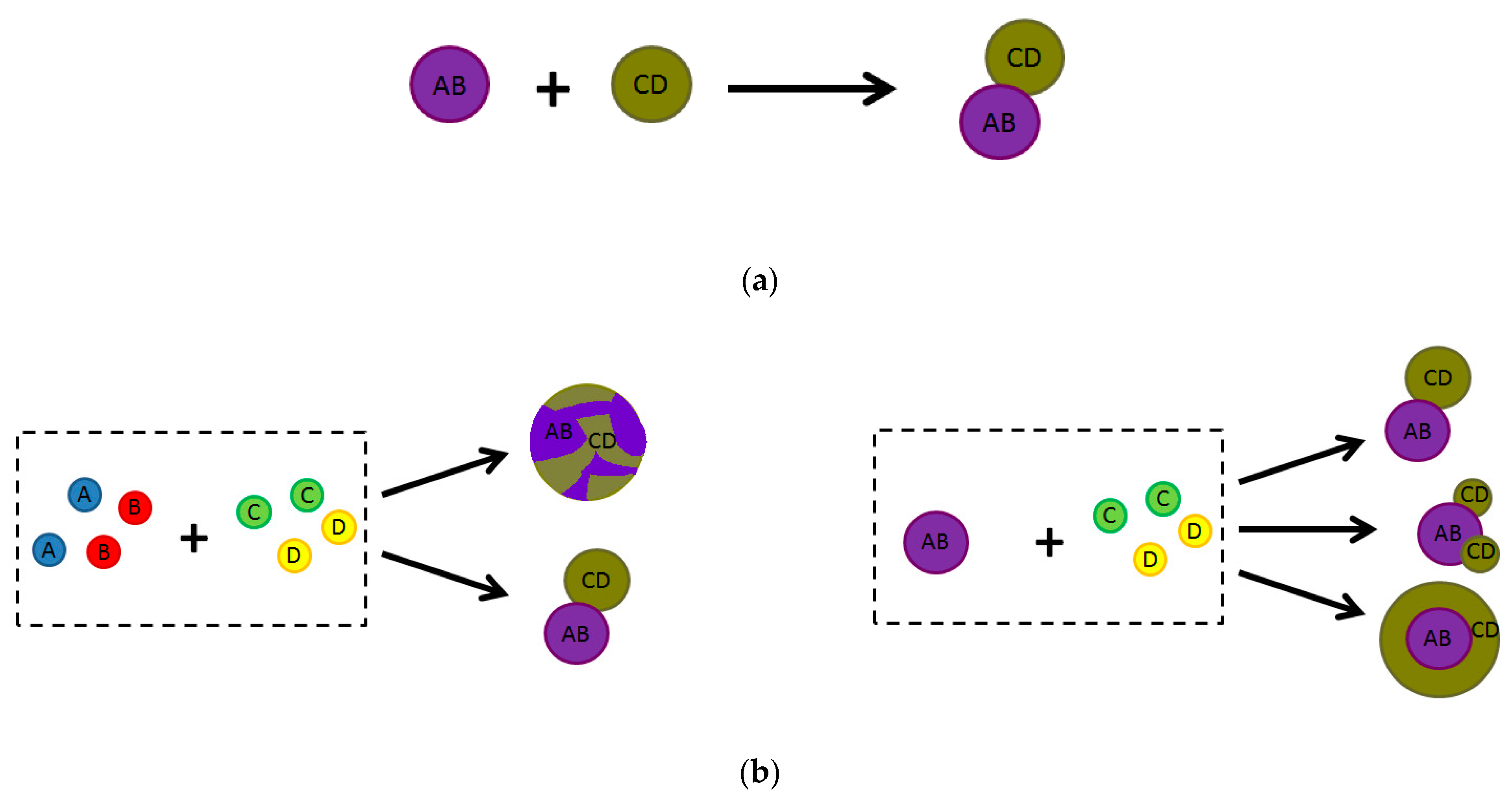
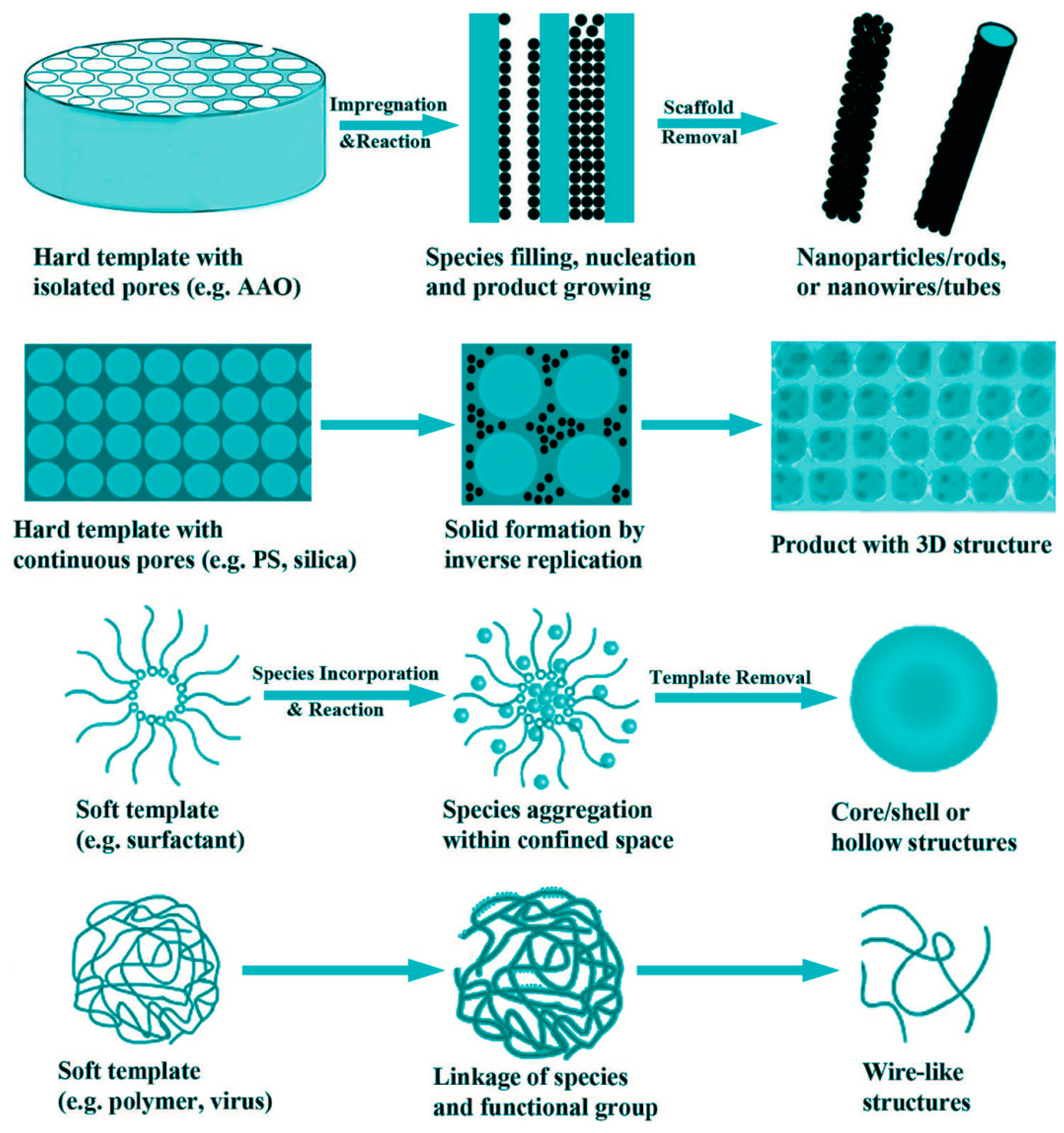
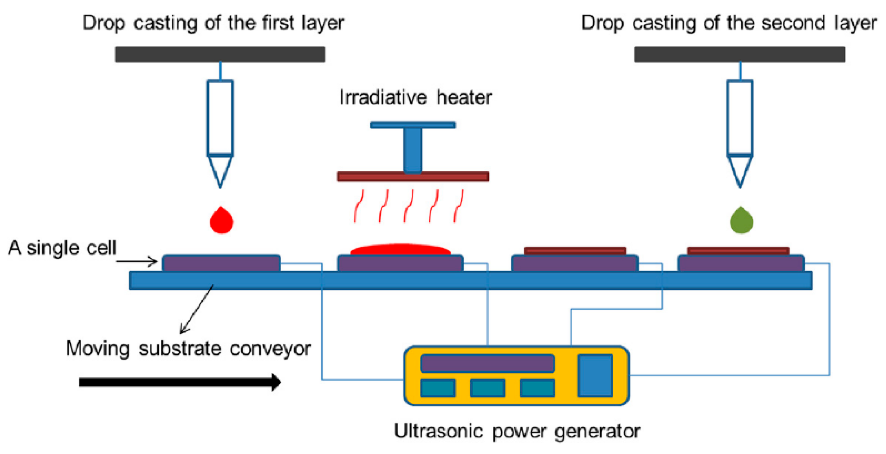
2. How Photoactive Heterostructures Are Made

In general, heterostructured photoactive materials can be divided into two major types: dispersed and deposited on various substrates (in particular, surfaces such as planar structures). Figure 3 demonstrates various heterostructured photoactive materials. The designs of these materials can be very unusual in form and composition. The heterostructured systems shown in Figure 3a–j represent the dispersed materials, and those in Figure 3k,l have a planar structure. Typically, dispersed photoactive materials are widely used in photocatalytic processes (such as water and air purification, disinfection, the recovery of metals from industrial wastewater and artificial photosynthesis) while deposited (planar) heterostructures are usually used as electrodes in photoelectrochemical systems, including fuel and solar cells. The latter can be used also as self-cleaning coatings.
The synthesis and heterostructure formation methods for the dispersed and deposited systems can be significantly different. Further, we consider the major methods of the synthesis and formation of heterostructured materials, indicating for which system they are more suitable.
Photoactive heterostructured materials can be formed via either one-pot (in situ) or multistep (ex situ) synthesis approaches. In the ex situ synthetic strategy (Figure 4a), the components of the heterostructured material are prepared separately in advance and then heterostructures are formed using a variety of techniques such as high temperature solid phase synthesis, drop-casting, sonication assembly, impregnation, ball-milling, sol–gel, or hydrothermal/solvothermal assembly methods, etc. An ex situ synthesis approach has many advantages including low cost and scalable production. However, the methods require multiple complex and time-consuming steps to prepare the individual materials and components of heterostructures. Moreover, it is difficult to control the preparation of the heterostructures, since their components are randomly dispersed with weak interactions. In these cases, it is imperative to verify the quality of the heterojunctions.
For an in situ synthesis strategy, the starting materials for one or all of the components of the desired heterostructure are mixed together for further treatment (Figure 4b). Since the synthesis process typically involves ionic reactions, this synthesis route leads to complex interactions and a uniform dispersion of components throughout the entire volume of the heterostructured material. That is why the one-pot synthetic strategy has attracted great attention from researchers in various fields of science, including material science and photocatalysis.
Methods for the synthesis of both heterostructured materials and their individual components can be classified in different ways. For example, all methods can be divided in two groups based on the type of nanostructure formation: the “bottom-up” approach is characterized by the growth of nanoparticles or the assembly of nanoparticles from individual atoms, and the methods related to the group “top-down” are based on the “crushing” of starting materials to nanosized particles or on the intercalation and exfoliation of nanosheets [20,38,44]. Several synthesis methods according to this classification and the possible types of the obtained nanostructures are presented in Table 1. “Top-down” approach methods are able to produce large amounts of nanostructured materials. However, controlling the size of the obtained nanomaterials is very difficult and expensive. The “bottom-up” approach takes advantage of physicochemical interactions for the hierarchical synthesis of ordered structures through a self-assembly of the building blocks. In this approach, particle morphology and size can be easily controlled. For example, graphene- and metal dichalcogenide-based layered composites are successively produced by exfoliation methods [45,46,47,48].
The major characteristics for another type of classification is based on the principles for producing and stabilizing a material [27]. According to this classification, synthesis methods can be conventionally divided into three groups: chemical, physical, and mechanical. However, clear borders between these groups do not exist. Thus, the mechanical methods ascribed elsewhere [27,49,50,51,52,53] are often proposed to be combined with chemical methods, and also used for the modification and activation of synthesized materials. Using mechanochemistry, particles with sizes of up to submicron (100–1000 nm) can be produced.
The application of the physical methods for material formation assumes that no new compounds are formed from precursors, although chemical bonds are formed during the growth of the nanostructures. Most physical methods are based on a “top-down” approach (see Table 1) [27]. Various types of lithography are intensively used for nanostructure fabrication [28,44,54,55]. Among the “bottom-up” physical methods, typical examples are molecular beam epitaxy and various methods of evaporation (physical vapor deposition (PVD), magnetron sputtering, plasma-enhanced deposition, laser ablation, electric arc deposition, etc.) followed by growth control in an inert atmosphere and the stabilization of the nanoparticles [45,53]. At the same time, it should be noted that when the particle growth occurs in an active gaseous atmosphere (for example, in the presence of oxygen to obtain oxide nanoparticles), then various chemical reactions can take place. Thus, such processes of material formation start from physical pathways and finish as a chemical reaction. The application of a “bottom-up” approach looks quite attractive, since self-assembly processes open up the possibility of forming rather large arrays of identical elements, and the size of these elements can vary within a wide range (for example, compared to what is currently available in lithography). However, the application of self-assembly processes has at least one drawback, such as packaging defects in the deposited particle layers.
Purely chemical methods involve chemical synthesis routes in which new substances are formed from their precursors. Widely used examples of chemical methods are sol–gel synthesis (including film formation by dip-coating and spin-coating methods from sols), synthesis in micelles (microemulsion approach), high temperature solid-state reaction, chemical precipitation or coprecipitation, chemical bath deposition, etc., i.e., facile methods of wet chemistry. These methods are reviewed in detail elsewhere [26,27,28,29,44,48,51,53]. Chemical precipitation carried out in an aqueous solution is straightforward and readily upgraded to an industrial scale [56,57,58]. However, as precipitation occurs in the entire volume, not all particles come into contact with the substrate. It also causes a wide particle size distribution and poor crystallinity that relies on additional processes such as solvothermal treatment. Hot injection produces particles with a narrow size distribution, but which need further professing to remove the stabilizers and/or organic linkers [59]. Chemical bath deposition is a method best suited for producing one-dimensional structures that have the advantage of increased surface area [60]. Unfortunately, this method is rather limited to several compounds and cannot be used for complex compositions. Summarizing all of the above, the advantages of the chemical methods include their simplicity and scalability, as well as their compatibility with a wide set of nanostructured compounds.
The most widespread methods applied to form heterostructures are physicochemical, in which nanoparticles are formed as a result of chemical reactions under the influence of various “physical” factors such as temperature, pressure, ultrasound and microwave irradiation, etc. These factors affect primarily the thermodynamic and kinetic parameters of the chemical process, but not the substances themselves. This results in the formation of materials with a specific microstructure, phase composition, and consequently, with unique functional properties. Remarkably, it is impossible to obtain a material with such properties carrying out a reaction without an appropriate “physical” impact (for example, see [28,61,62]).
This group includes solvothermal synthesis (sometimes ultrasound-assisted) [27,28,44,51,53,63], microwave-assisted synthesis [26,27,28,44,53], photodeposition [29,44,64], synthesis in supercritical solvents [65], aerosol pyrolysis (spray pyrolysis and laser pyrolysis) [26,27,53,66], chemical exfoliation [53], and methods for nanoparticle or film growth from the gas phase (chemical vapor deposition [26,27,44,51,53,67], atomic layer deposition [48], etc.), the growth of nanostructures by the liquid-crystal mechanism (hot injection [29], successive ionic layer adsorption (SILAR) [29,68] and other methods of layer-by-layer deposition [26,28,44,69]).
Therefore, one can infer that the formation of heterostructured materials with high-quality heterojunctions typically requires a combination of the various methods and techniques (even for in situ synthesis). The selection of the appropriate synthesis method can produce heterostructures with the desired performance. To solve specific synthetic problems, one can be guided by previously accumulated experience (for example, the preparation of mixed-phase heterostructured photocatalysts has already been described for TiO2 [70] and BiVO4 [71]). Today, the scientific literature contains excellent reviews on the synthesis of various heterostructures based on different metal oxides and chalcogenides [28,29,72], hematite [73], layered double hydroxides [74], graphene [45,46,47,48], and quantum dots [65,75].
In the set of various physicochemical methods, electrochemical deposition takes a special place [29,44,53]. It involves chemical reactions in an electrolyte solution when a potential bias is applied to the conducting substrates (metal, FTO or ITO glass). Electrochemical deposition is relatively simple and scalable for the production of planar systems with high-quality heterojunctions in a controllable and directed way. Electrodeposition can be used to form heterostructures with complex morphologies in a highly controllable manner, though it requires an advanced deposition setup.
The fabrication of some hierarchical composite structures, such as core-shell [26,44,66,76] and hollow [44,77] structures, requires an application of the specialized synthetic techniques. The template-assisted method is worth mentioning [44,78]. The employed materials in template synthesis can be simply classified into hard templates (anodic aluminum oxide or silica, possessing well-confined void, which is in the form of channels, pores, or connected hollow space) and soft (consists of organic surfactants, polymers, and even biological viruses, which are relatively flexible in shape) templates. Figure 5 shows some typical examples of the hard and soft template synthesis of electrode materials with diverse morphologies. The overall process generally involves the following procedures: (1) precursors combine with templates by impregnation or incorporation; (2) solid species form through reaction, nucleation and growth; and (3) product is obtained after template removal. Templates can be employed for various synthetic techniques such as sol–gel synthesis, chemical vapor deposition, thermal decomposition, electrodeposition, solvothermal preparation, and so on.
Recently [79], a simple, low-cost, versatile, and potentially scalable casting method was proposed for the fabrication of micro- and nanofilms, termed ultrasonic “substrate vibration-assisted drop casting”. Imposing ultrasonic vibration on the substrate can convert the uncontrollable drop casting method into a controllable coating process. Figure 6 illustrates the scheme of the suggested technique. The maximum effective and uniform surface area that can be obtained for application in a device depends on the surface wettability, solution properties, impingement conditions, and substrate vibration.
It is wise to note that the quality of the resulting heterostructured material, both in dispersed and in deposited form, is significantly affected by such factors as the affinity of heterostructure components (the values of surface free energy, adhesion, surface wettability) [44,55,80], the roughness of the substrate or previously formed layer or component, the formation of the intermediate layer between different components [81], the acidic–basic conditions of the reaction media (especially for the components of heterostructure with different points of zero charge) [29,64,71], the reaction temperature [24,82], the organic binder, surfactant and organic solvent (mainly in the synthesis from solutions, for example, in solvothermal technology) [76,80,82,83,84], etc.
The effect of the reaction temperature on the morphology of monolayer MoS2-WS2 lateral heterostructures has been demonstrated by Liu and coauthors [24]. It was convincingly shown that the size of as-formed heterostructures synthesized via the chemical vapor deposition method proportionally increases with the reaction temperature, which can be explained by the enhanced vapor pressure and reactivity of precursors at elevated temperature. Thus, at the precursor weight ratio (MoO3:WO3) of 1:100, a large size of lateral heterostructure of about 560 µm was obtained at a high temperature of 750 °C. At reaction temperatures above 800 °C, the WS2 stripe embedded in the MoS2 matrix was formed, opening up an easy way for the fabrication of quantum well structures.
The acidity of the reaction medium as an example of influencing factor, is considered below [29]. An optimal pH value for heterostructure formation can be found by measuring the point of zero charge or the ζ-potential value of individual nanoparticles at different pH. Figure 7 demonstrates ζ-potentials of g-C3N4 and Zn2GeO4 nanoparticles in water as a function of acetic acid concentration. As one can see, at a given acid concentration materials exhibit distinct (either positive or negative) ζ-potentials. The region where nanoparticles have opposite charge is then considered as an optimal condition for aggregation.
Finally, it is worth mentioning the scaling issues for some synthesis methods. Many of the “bottom-up” methods for the synthesis of nanomaterials are based on solution synthesis, in which precursor concentrations are usually very low (typically, in the millimolar range). Scaling up these synthesis approaches to produce commercial-scale quantities is expected to introduce significant challenges for control of particle size, morphology, and structure. This aspect of nanomaterial synthesis is still in its infancy and offers new exciting research endeavors in the area of photoactive heterostructured materials.

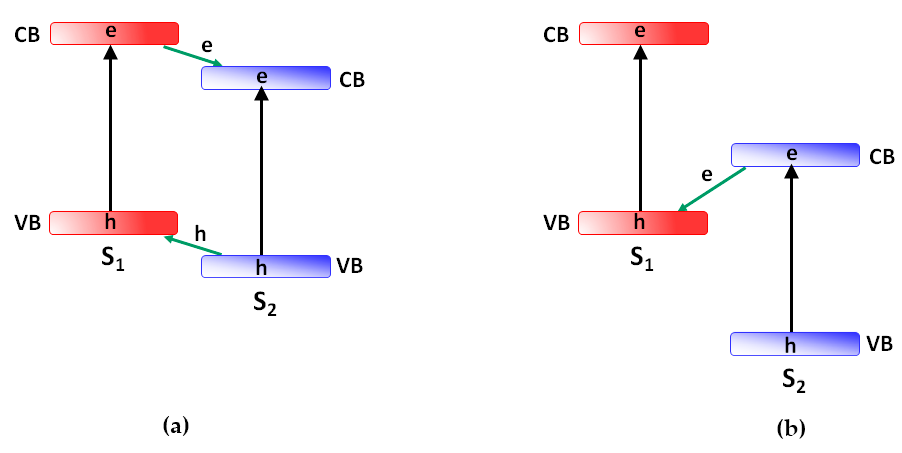
3. How They Are Explored

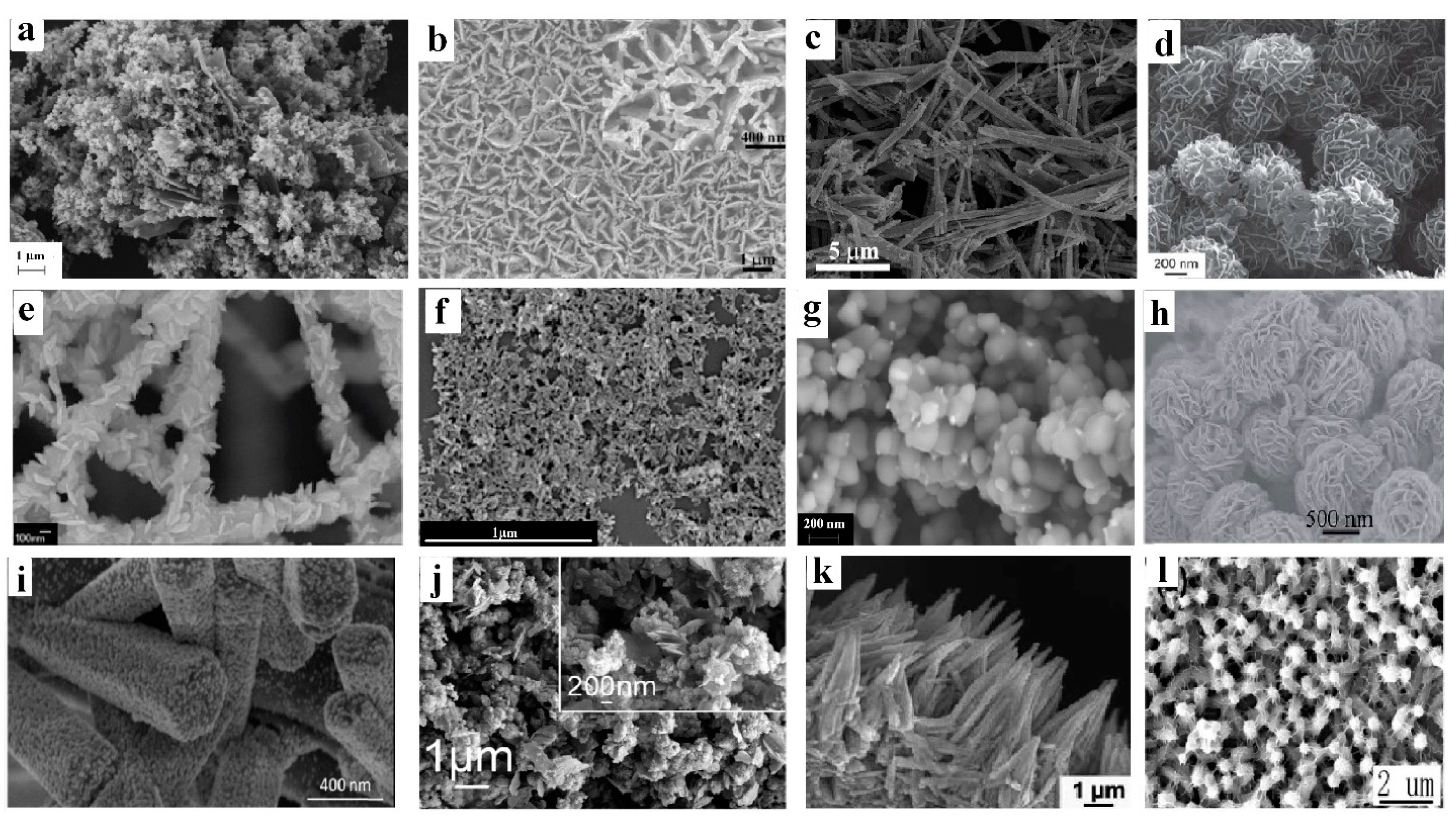
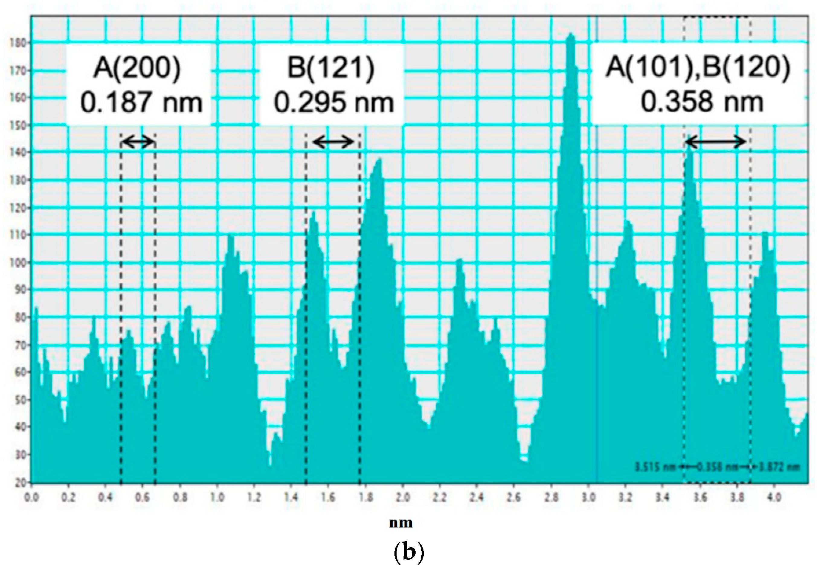
3.1. Electron Microscopy

After the synthesis of a material believed to be a heterostructured material, an absolutely necessary action is to confirm the successful formation of a heterostructure. A distinguishing feature of a successfully formed heterostructure is the observation of a strong, dense and defect-free heterojunction between heterostructure components. The main direct method to prove a heterojunction formation is the observation of images of the interface zone between the heterostructure components using high-resolution transmission electron microscopy (HRTEM). The principles of transmission electron microscopy techniques for imaging and compositional evaluation in semiconductor heterostructures have been described elsewhere [85]. The presence of the fringes with several lattice spacings corresponding to the components of the studied composite material indicates that the components are well contacted and, therefore, an interface of heterostructure has been successfully constructed. Figure 8 shows several examples of formed intimate heterojunctions. The lattice fringes make it possible to identify crystallographic spacings corresponding to a specific plane of a given crystal solid. For example, in the HRTEM image of Bi2MoO6/Zn–Al layered double hydroxide (LDH) (Figure 8a), d-spacing value of 0.192 nm corresponds to the (018) plane of LDH, whereas the d values of 0.166 nm represent the (331) plane of the orthorhombic phase of Bi2MoO6 [86].
HRTEM images are often accompanied by electron diffraction patterns (selected-area electron diffraction (SAED) convergent-beam electron diffraction (CBED) or precession electron diffraction (PED)) [20,23], suggesting the highly crystalline nature of the given sample. From the technical point of view, electron diffraction is readily available on any transmission electron microscope where it can be further combined with other complementary techniques such as imaging and/or X-ray spectroscopy. Moreover, electrons are scattered by light atoms relatively more strongly, and electron diffraction patterns can show reflections corresponding to a resolution beyond that available with X-rays. It is wise to note that the typical size of an area studied by SAED is a few hundred of nanometers; with CBED, the areas studied are limited by the beam size and the beam interaction volume (approximately 10 nm) [87,88,89,90].
By definition, electron diffraction patterns reflect a reciprocal lattice structure of solids. Consequently, in the heterojunction area one can see either a combination of electron diffraction patterns of heterostructure components (for a close to ideal heterojunction with a sharp boundary) or the traces of the new pattern corresponding to the structure of a spatially extended heterojunction. Examples of the electron diffraction patterns are shown in Figure 9 and Figure 10.
Figure 9 demonstrates electron diffraction patterns of VO2/NiO/c-YSZ/Si (here c-YSZ denotes cubic Y stabilized zirconia) heterostructures for different thicknesses of VO2 epitaxy grown film [91]. The crystallographic alignment across the interfaces was established to be VO2(010)||NiO(111)||c-YSZ(100)||Si(100) and VO2(100)||NiO(110)||c-YSZ(100)||Si(100). Particularly, the analysis of the electron diffraction patterns inferred that the increase in the VO2 layer thickness results in the relaxation of the VO2||NiO interface due to the decrease in the lattice misfit strains caused by the formation of dislocations at the surface of the thicker layers.
The data presented below (Figure 10) demonstrate the importance of the TEM method for the characterization of heterostructured materials. The aim of the presented experimental studies was to determine whether the mixed-phase TiO2 nanomaterials are a simple physical mixture or whether each individual nanoparticle consists of more than one phase forming heterojunctions. For this purpose, three mixed-phase (anatase (A), rutile (R), and brookite (B)) TiO2 nanoparticles were probed by transmission electron microscopy.
According to the HRTEM images in Figure 10a(ii) [70], d spacings from different TiO2 phases can be observed, hence providing direct evidence of the intraparticle mixed-phase nanomaterials. The analysis of A/b, B/r and R/b in terms of the presence of the characteristic d-spacings demonstrates a coexistence of the corresponding phases A–B, B–R and R–B. Further evidence of the mixed-phase character of the synthesized TiO2 photocatalysts is revealed by the SAED patterns shown in Figure 10a(iii). The continuous ring patterns indicate the anatase-major, brookite-major, and rutile-major particles to be polycrystalline, judging from the concentric Debye–Scherrer rings which can be indexed to (111) and (101) for anatase, (121) and (120) for brookite and (211) for rutile. More specifically, using the DigitalMigrograph software, the HRTEM images of all three mixed-phase materials were analyzed by taking lattice profiles at three different spots of <4 nm size. Thus, as can be seen in the case of A/b (Figure 10b), the characteristic A (101), A (200) and B (121) and B (120) planes are present within 2–3 nm space, i.e., in a distance smaller than the size of a single nanocrystallite.
The phase composition can be additionally confirmed by the X-Ray diffraction (XRD) method and Raman spectroscopy. However, it wise to remember that these widely used methods provide information neither about the formation of the interface nor about the quality of the heterojunction. Chemical information obtained by electron dispersive X-ray spectroscopy (EDX or EDS) allows unequivocal recognition of the heterostructure components using an element mapping that provides element distributions over both sides of the heterostructure interface [20,21,22,23].
Therefore, the images obtained by the HRTEM technique combined with electron diffraction patterns provide strongly necessary evidence of the successful formation of the heterojunction in heterostructured photoactive materials. Note that the SEM images typically used in many studies cannot prove the formation of a heterojunction as they show only a presence of the “physical” contact between different components, providing no data about the quality of any interface between them.

3.2. Optical Characterization

The optical properties of photoactive materials play a key role in their fundamental behavior and practical functionalities. Indeed, a starting point of photocatalytic processes, which particularly those determining the photoactivity of materials, is light quantum absorption. The absorption by solid material of light quanta of the UV-VIS-NIR spectral region results in the process of electron transition from the ground state to the excited state of solids. Thus, optical measurements are often used in studies devoted to the electronic structure of investigated materials. Strictly speaking, an electron structure of solids determines the probability of the light quanta absorption in accordance with the solid electronic structure and the selection rules of electronic transitions from the one (ground) state to another (excited) state(s) due to a perturbation caused by light electromagnetic waves (or photons). The corresponding theory is well developed and described in detail in the framework of quantum mechanics. The ground and excited electron energy levels can form both the bands of delocalized electron states (valence and conduction bands) and the localized energy levels (for example, localized electronic states of impurities and defects within the bandgap of solids).
The backward process is the relaxation (or recombination) of the excited state of solids, during which the energy of the excited state may be transformed into either heat or into new light quanta (luminescence). The time period between the excitation and relaxation processes is called the lifetime of the excited state. In the photoactive materials used in heterogeneous photocatalysis and photoelectrochemistry, the most essential type of photoexcitation results in the generation of free charge carriers. During their lifetime, photogenerated charge carriers can migrate toward the surface and initiate interfacial chemical transformation sequences by interaction with molecules adsorbed at the surface or located near the surface of photoactive materials due to the charge transfer process. At the same time, during their migration in the bulk and at the surface of solids, photogenerated charge carriers can recombine with each other, be trapped by impurities and defective states or drift in an applied electric field. This results in a set of various photostimulated phenomena such as photoluminescence, photochromism, surface photochemical activity, photoconductivity, etc. Whatever a photoresponse effect caused by solid photoexcitation is, all of them start from light absorption. In turn, it means that experimental studies of such materials and phenomena require an application of the correctly performed optical measurements.
In accordance with the energy conservation law, the intensities of the incident (Io), transmitted (IT) and specular reflected (IR) beams are then related as shown by Equation (1),
Io = IR + IT + IA
where IR, IT, and IA are the intensities of the reflected, transmitted and absorbed light, respectively. They can be described with the corresponding coefficients R, T, and A representing the fractions of reflected, transmitted and absorbed light with respect to the actinic light.
IR = R Io
IT = T Io
IA = A Io
Thus, from Equations (1) and (2) it is clear that the dimensionless coefficients R, T and A, that refer, respectively, to reflectance, transmittance and absorbance satisfy Equation (3),
R + T + A = 1
It is also known from experience that for optically uniform solid plate with a thickness d (Equation (4)),
I T = ( 1 R ) I o   e α d
Accordingly, from Equations (2a–c) and (3) one obtains Equation (5):
T = ( 1 R ) e α d
A = ( 1 R ) [ 1   e α d ]
In the general case,
I ( x ) = ( 1 R ) I o   e α x
where I(x) is the intensity of the light beam at a distance x from the illuminated surface. The latter equations (Equations (5) and (6)) represent the Lambert-Bouguer law for absorbance (of a solid parallel plate of thickness d). The entity α is known as the linear (Naperian) absorption coefficient (its dimension is the inverse length with typical units of cm−1). It is wise to note that the absorption coefficient is an intrinsic optical characteristic of solids. Indeed, the intrinsic electronic structure and optical band gap are unequivocally defined by the chemical composition and crystal structure of solids. At the same time, the absorption coefficient within fundamental absorption spectral region of a solid is absolutely dictated by the band structures and the band gap (following the selection rules for electronic transitions between different electronic states in the bands and energy and momentum conservation laws) and therefore, is a fundamental characteristic of solids.
However, in practice for measurement of the absorption coefficient of a nonscattering medium (such as a solid single crystal plate) a double beam spectrophotometer is used. An absorbance A (or optical density) value provided by the spectrophotometer is the result of a calculation based on the data on transmission, i.e.,
A = −log10 T = −α’d.
It is important to note that the logarithm in this calculation is a decimal one and the absorption coefficient α’, calculated for solid plate of the thickness d, is called a decimal absorption coefficient (Equation (8)):
α = log 10 ( I I 0 ) d
Typically, an absorbance (optical density) of optical materials (glass filters, crystals, etc.) presented in catalogs is calculated by Equation (7). The decimal absorption coefficient α’ could be easily recalculated to the natural α by the formula α = ln10 α’ ≈ 2.303 α’. This fact must be attentively taken into account for the correct application of the absorption coefficient values obtained from somewhere else in the further considerations. However, by definition an absorption coefficient for solids as their fundamental optical characteristic is determined by Equation (4). Particularly, the linear (Naperian) absorption coefficient is used to describe the spectral dependence α(hν) at the edge of the fundamental absorption.
Should either the direct or indirect band-to-band electronic transitions correspond to the parabolic part of the Brillouin plot for both valence and conduction bands, the dependence of the absorption coefficient on the energy of the actinic photons is given by Equation (9):
α ( h ν ) = const ( h     E g ) m h ν
where Eg is an optical band gap of semiconductor, and m = ½ for direct transitions, and m = 2 for indirect transitions. Accordingly, the transformation of Equation (9) to the form of Equation (10) infers that α(hν) = 0 at hν = Eg which, in turn, provides an estimation of the optical band gap of a solid by applying a linear approximation for the transformed absorption spectrum at the edge of the fundamental absorption.
( α ( h ν ) h   ) 1 / m = const ( h   E g )
However, in practice the photoactive materials (either photocatalysts or photoelectrode materials) are highly dispersed and, therefore, represent strongly light scattering media. Consequently, the direct measurement of the absorption spectra is not possible and one is forced to apply diffuse reflectance spectroscopy to measure a diffuse reflected light [92,93] (or diffuse reflection coefficient).
There are two type of reflection: regular or specular (mirror) reflection, for which the term reflectivity is often used; and reflectance, in which the angular distribution is isotropic and independent of the angle of incidence [92,94]. The last term is also called diffuse reflectance.
For the measurement of diffuse reflectance, a double beam spectrophotometer is equipped with a special accessory—an integrating sphere [93,94]. Diffuse reflectance spectroscopy is an irreplaceable method in the experimental measurements of the optical absorption of powdered solid specimens. For instance, the absorbance A of a sample and the diffuse reflectance coefficient are correlated as defined by Equation (11); that is,
A = 1 − R
provided that the transmittance of the system T = 0, which in practice is valid when the thickness of the powdered sample is ca. 3–5 mm.
The reflectance spectrum R(λ) measured by spectrophotometer is a ratio of light intensities reflected from the sample, Is(λ), and that reflected from the reference, Iref(λ).
R ( λ ) = I s ( λ ) I ref ( λ )
Note that mathematically Equation (12) is the same as Equation (2b). It means that a spectrophotometer technically cannot recognize and does not know what exactly is being measured: either transmittance or diffuse reflectance. However, physically there is a great difference between these two optical characteristics. Therefore, it is absolutely physically incorrect to set a spectrophotometer in regime “absorbance” measurements while measuring diffuse reflection. Unfortunately, this is a typical experimental mistake in the optical characterization of photoactive materials.
It should be also emphasized that diffuse reflection coefficient R(λ) in Equation (12) is a relative parameter which is defined with respect to diffuse reflection of the reference sample and is not equal to the absolute reflection coefficient R used in Equation (3). The materials with reflectance properties close to the ideal (that is Rref ≈ 1) in a required spectral range (for example, magnesium oxide, barium sulfate, sodium chloride [94] and others) are used as the reference samples. However, even their diffuse reflectance is not equal to 1 across the whole spectral range. In other words, the absolute diffuse reflectance coefficient of the studied material, R, is R = R*R∞(ref), where R* is the diffuse reflectance coefficient measured by the spectrophotometer and R∞(ref) is the absolute diffuse reflectance coefficient of the reference sample. Therefore, one should know the spectral alteration of the diffuse reflectance of the reference sample to calculate an absolute diffuse reflectance spectrum of the studied photoactive materials. This fact is typically ignored by researchers in the fields of photocatalysis and photoelectrochemistry, which often leads to incorrect data presentation and conclusions. It is especially important when diffuse reflectance spectra are used for their further development and transformation in the form of Kubelka–Munk function and Tauc plot. In both transformations an absolute diffuse reflectance coefficient must be used.
A theory of light scattering for description of diffuse reflectance was developed by Kubelka and Munk [95]. The Kubelka–Munk theory was described for the first time in 1929 in a research paper of the Spolek pro chemickou a hutni vyrobu (Chemical and Metallurgical Works) at Aussig (Usti) and then published in Zeits. F. Tech. Physik in 1931 [95]. Later, the theory was described in English by Steele [96] and the Steele’s abstract was recommended by Paul Kubelka for familiarization with the basis of Kubelka–Munk theory [97]. The description of the Kubelka–Munk theory has been also presented in the works [92,93,94].
The model is referred to a “continuum theory’, which is based on the concept of a homogeneous medium layer with absorption coefficient k and scattering coefficient s referred simply to unit path length. The model does not include the real properties of particles (size, shape, refractive index, absorption coefficient) as well as the change of wavelength distribution by specific absorption or by dispersion [95,97]. It is assumed that an infinitely thick layer is irradiated with diffuse monochromatic light from one side, and inside the layer light propagates the medium in both forward and backward directions diffusively [95,97].
As a result of the KM modeling, the relation connecting the absolute diffuse reflectance R of an infinitely thick layer, its absorption k and scattering s coefficients are obtained:
f K M = k s = ( 1 R ) 2 2 R
where fKM—is Kubelka–Munk function, k—absorption coefficient (cm−1), and s—is scattering coefficient (cm−1).
Although a number of other similar equations were developed at that time [98,99,100,101,102,103], they are generally considered as specific cases of the general Kubelka–Munk theory [104]. The extended forms of the Kubelka–Munk function for various particular cases—sample thickness, scattering and absorption properties, nonhomogeneous medium—were presented in the later works by Kubelka [97,104]. Further considerations of diffuse reflectance in the framework of the “discontinuum theory” (i.e., including the structure of a medium, index of refraction, etc.) are presented elsewhere [105,106,107,108,109,110,111,112]. A question about k included in Equation (13) was also raised: is k equal to absorption coefficient α? For example, Kortum considered these constants as equal [92,94], while Simmons [103] derived for particles of size d with the refractive index n and absorption coefficient α the equations:
k = 2n2α/3
and
s = 1/d
In general, the constant k in Equation (13) may be considered only as being proportional to α [103,112].
The Kubelka–Munk theory predicts that the KMF is proportional to the concentration C of the absorbing species as long as the main assumptions of the theory are fulfilled, namely that the absorbance of the sample is not too high and the absorbing species are distributed uniformly. Note that these two conditions must be strongly satisfied for the correct application of the KMF treatment. Obviously, in general, the latter condition concerning the uniform distribution of the absorbing species is not fulfilled for heterostructured materials composed of at least two different materials possessing different optical properties.
Because of their extreme simplicity, KM functions are quite attractive. In this regard, we should note that even the main assumptions of the theory are not often fulfilled in actual experiments. For example, calculation of the KMF from R(λ) in the range of hν ≥ Eg, which is in the range of strong absorption, is incorrect. The Kubelka–Munk two-flux radiative transfer model is strictly applicable only to the case of the diffuse illumination of a sample, but is often applied in the case of collimated illumination used in a spectrophotometer. When collimated illumination is examined, the theory of light propagation in dispersed media loses the above-mentioned simplicity [97,113]. Another typical mistake in the practical application of KMF is the assumption that KMF corresponds to the absorption coefficient by ignoring the spectral dependence of the scattering coefficient. In fact, the spectral dependence s = fn(λ) of the light absorbing media can be far more complex. Again, dealing with heterostructured materials, one should keep in mind that each component of a heterostructure possesses its own optical characteristics and therefore the application of the KMF treatment for such materials is physically invalid.
At the present time, a typical approach to determine an optical band gap of dispersed photocatalysts used by many researchers is the so-called Tauc plot method. Remarkably paradoxical, the original work by Tauc [114] considered the optical spectra of amorphous solids and did not concern crystal solids. Moreover, the original Tauc plot method was applied to determine the optical band gap (not an edge of absorption) of amorphous solids for the spectral region of strong fundamental absorption (α ~ 104 cm−1) where light absorption corresponding to the amorphous states of solids became negligible compared to the absorption originating from the band-to-band transitions, and where the light absorption was too strong for the reliable application of diffuse reflectance spectroscopy. Nevertheless, mathematically, the Tauc plot model coincides with Equations (9) and (10), which are valid at lower values of the absorption coefficient at the edge of the fundamental absorption of crystal solids. Thus, the correct approach to determine the optical band gap using diffuse reflectance spectroscopy is a combination of Equations (9) and (10) and the Kubelka–Munk model. It is based on the substitution of the absorption coefficient in Equations (9) and (10) by the Kubelka–Munk function (KMF) which, as assumed, is proportional to the absorption coefficient. Concomitantly, in most cases the conditions of validity and reliability of KMF and the Equation (9) are completely ignored as well as the fact that a “Tauc plot” is just a mathematical treatment of the diffuse reflectance spectra that does not provide a physical sense of these spectra. The correct application of the Tauc plot method to estimate (not to determine) the optical band gap requires the absolute fulfillment of the following three conditions:
  • The absorption in the given spectral range corresponds to the edge of the fundamental absorption and not to another type of light absorption by the solids (such as surface or extrinsic absorption);
  • The electronic transition between valence and conduction bands is either direct or indirect and a dependence of density of states on the energy near the top of the valence band and bottom of the conduction band is a square root dependence (that is characteristic for crystalline solids);
  • The conditions for the application of the KFM approach are completely fulfilled for the treatment of the experimental diffuse reflectance spectra (this is especially true for the requirement of the optical uniformity of the dispersed samples).
The latter conditions are often ignored. In particular, this makes the application of KMF and the “Tauc plot” treatment physically meaningless for heterostructured materials since such materials are not optically uniform by definition. In fact, all information which can be derived from the diffuse reflectance spectra of heterostructured materials is an observation of the difference between the diffuse reflectance spectra of heterostructured materials and their individual components. Otherwise, a development of the specific light propagation models is required for each studied heterostructure taking into account its spatial construction and the morphological and optical properties of the components.
In other words, heterostructured materials can be optically characterized correctly by original diffuse reflectance spectra (R(λ)). The application of KMF (and consequently so-called Tauc plot methods) to characterize the optical properties of heterostructures are physically incorrect since by definition, heterostructures are optically nonuniform materials. It is strictly necessary to indicate which material was used as a reference sample to measure diffuse reflectance spectra.

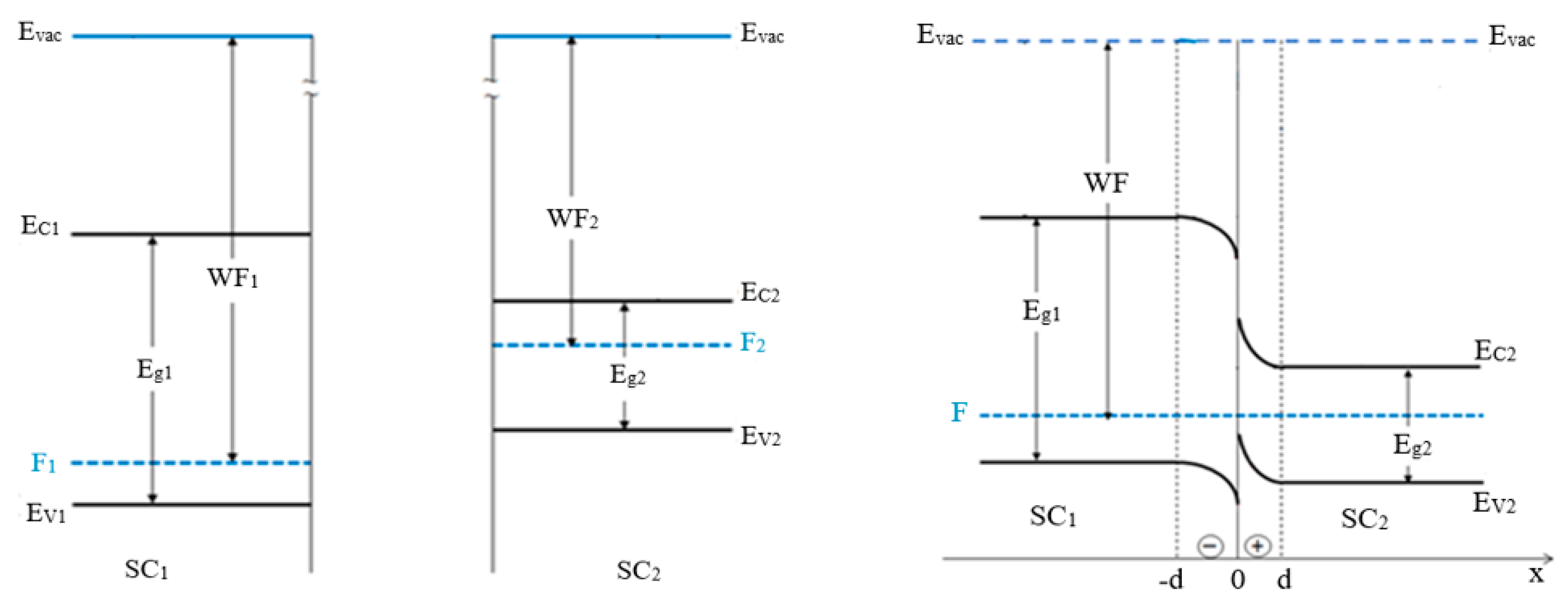
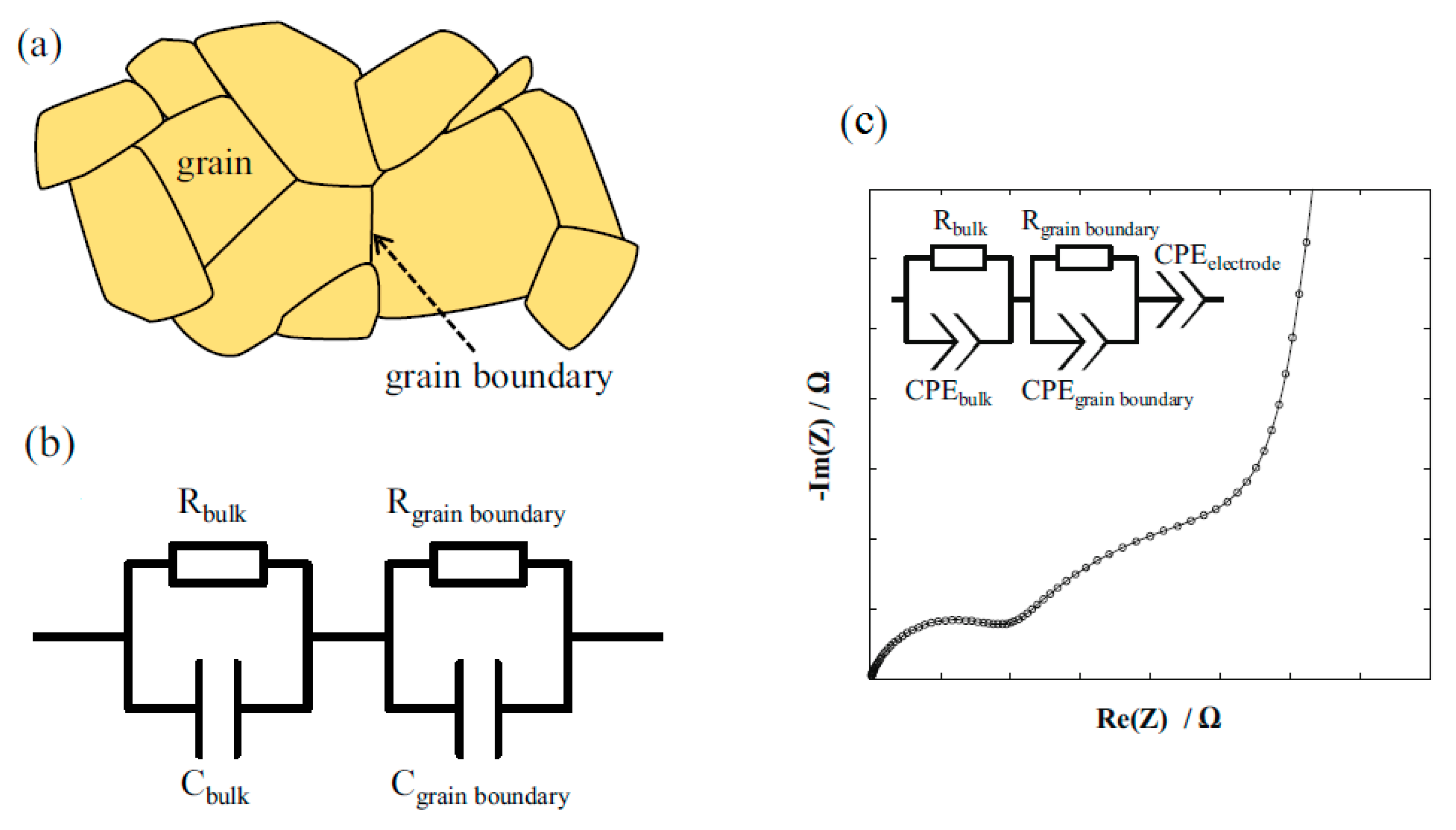
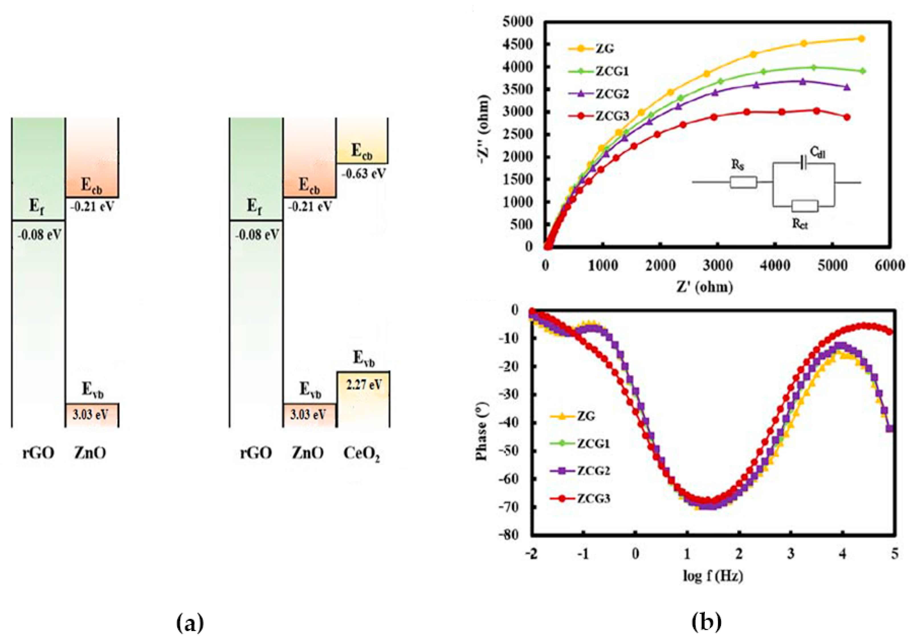
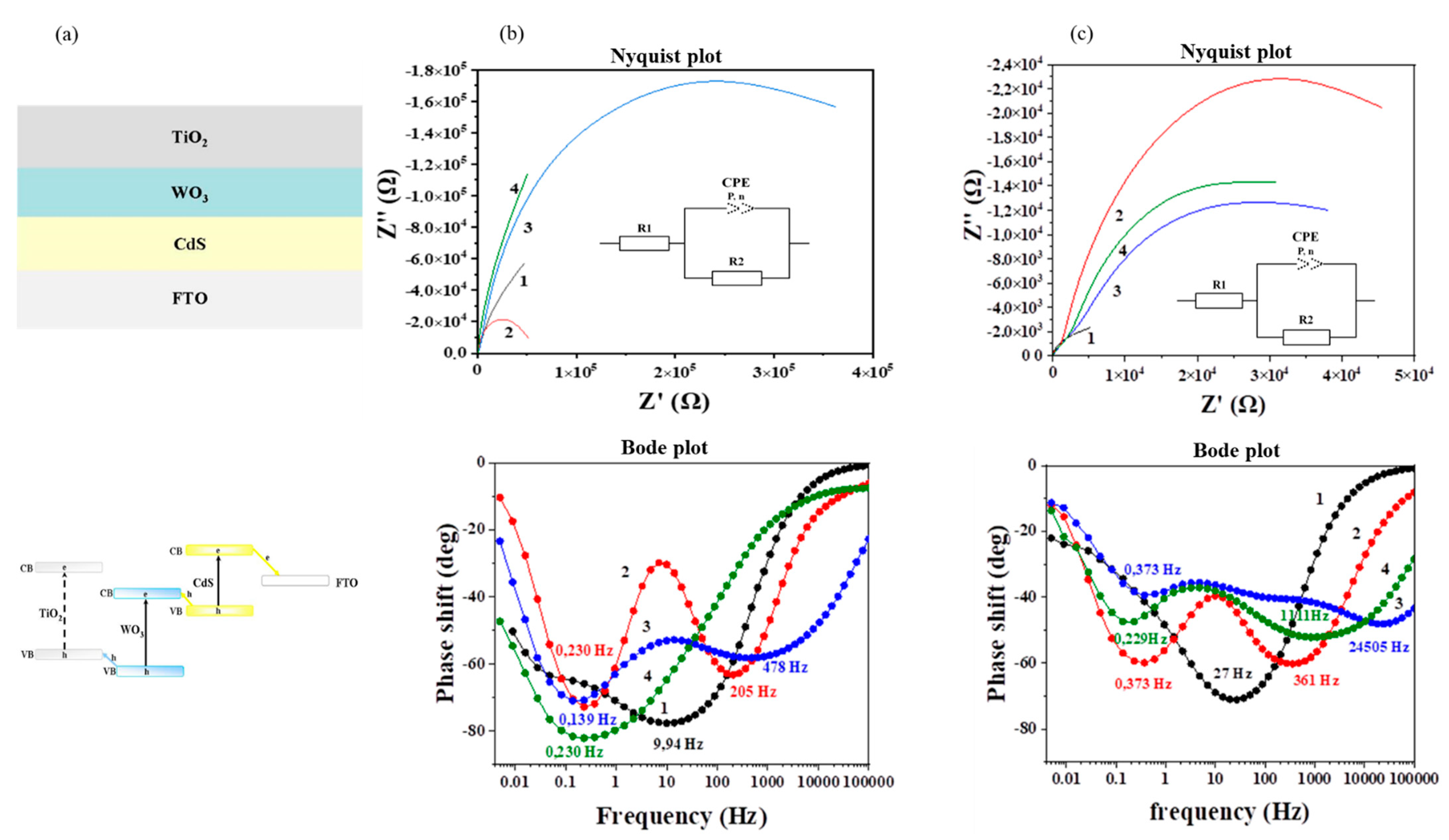
3.3. Electrophysical Characterization

A simple method to verify the successful formation of a heterostructure based on semiconductors, is a measurement of the work function of a heterostructure and its components. This method is based on the effect of the alteration of the work function caused by the redistribution of the charge carriers when a heterostructure is formed and the establishment of a new thermodynamical equilibrium state in heterostructure, comparing to its components and characterized by overall Fermi level and work function as demonstrated in Figure 11.
Since the formation of a heterostructure results in charge redistribution between its components, it leads to the establishment of a new Fermi level position in the heterostructure which is higher than in one component and lower than in another component. Consequently, a work function value of the heterostructure becomes located between the work functions of the individual components that is, WF1 > WF > WF2 (see Figure 11). Such an alteration of the work function value clearly indicates a formation of heterostructured materials as a united thermodynamic system.
The work functions of materials can be measured by the Kelvin probe technique. However, the application of this method has certain limitations: since the method is based on the oscillating capacitor system, the heterostructure material must have a flat surface morphology. That means that the photoactive heterostructured materials should be either in the “sandwich like” form (layer by layer) [115] or pressed in the form of plate [116].
Otherwise, work function can be measured using another experimental approach based on the application of UV or X-ray photoelectron spectroscopy [117,118,119]. It is important to note that in this case Fermi level positions and work functions must be measured and presented as absolute values with respect to vacuum level (not as relative values with respect to the Fermi level of the setup).
The electrochemical impedance spectroscopy (EIS) technique is another one of the most accessible and informative methods for studying electrochemical and electrophysical processes in different types of materials. This method proves to be extremely informative in various fields of electrochemistry, physics and materials science. In recent years, a broad variety of approaches have been successfully developed, allowing researchers to obtain unique information both on the properties of the systems under study and on the mechanisms of various photoprocesses [120,121,122,123,124].
The EIS method is based on the analysis of the dependences of the electrical impedance value of the studied system, as well as its components, on the frequency of the alternating current flowing through it. In addition to information on the direct current electrical conductivity of the system, this technique allows one to obtain information on the resistance of its components and the contributions of existed interfaces, as well as the resistances and capacitances of the boundaries between the particles forming the system [120,125,126].
The Z(ω) dependence analysis method, in general, is based on constructing equivalent electrical schemes—these being the model electrical circuits made of idealized circuit elements, such as resistance, capacitance, inductance, etc.—having the same frequency total impedance dependence compared to the sample under study. The equivalent substitution scheme type is determined not only by the properties of the system, but also by the frequency range in which it is investigated. Expanding the frequency range may lead to adding new elements to the equivalent circuit. Experimental techniques and data analysis are described in detail elsewhere [121,125,126,127]. One of the most serious problems of the experimental practice is the presence of the imperfect electrode contacts on solid material [128].
Initially, the basic principles of the impedance spectroscopy method were developed for ideal “single crystal—liquid electrolyte” systems, where the components were considered as bulk homogeneous phases with constant physical and chemical properties throughout the entire volume. [120,121] However, many real photoelectrochemical systems are by their nature polycrystalline solids. These materials have a lower real density compared to the theoretical density (due to hollowness) and disordered grains (which is important for anisotropic materials). In the simplest case, these effects will lead to a decrease in conductivity relative to a single crystal. In addition, various types of impurities can be present at the grain boundaries as a second phase, which also leads to a change in their properties [129,130]. The charge also transports properties of the complex systems that are controlled by imperfections, expected to exist there in higher concentrations than in the center of a grain, leading to an additional contribution to the intergrain impedance value. However, the relatively small difference between the absolute conductivity values does exist, most probably due to the geometric anisotropic effects of the material, as well as the preferential particles orientation in the pressed powdered sample.
The transport properties of lithium-ion conducting Li3xLa2/3-xTiO3 material were presented in [115] and were studied for bulk and grain-boundary effects. It was found that the intergrain boundary conductivity effect has greater activation energy and disappeared at higher temperatures. This interplay between the bulk and grain boundaries’ conductivity contributions can be modeled by an equivalent circuit model (Figure 12a,b) [130]. The Rbulk value thereby describes the intragrain conductive properties and the Cbulk value shows the dielectric properties, triggered by localized opposite charges such as lithium vacancies and lithium ions. Rgrain boundary resistance represents the value of the inner grain conductivity, while the C grain value characterizes the capacitance of grain boundaries partially blocked by impurities. Eectrochemical impedance spectroscopy (EIS) is a common analysis method of the intra- and intergrain processes in systems. In reality, the semicircles presented by the Nyquist plot, obtained for such a system, become depressed and the capacitive branch is not ideally perpendicular to the Nyquist diagram’s real axes, as shown in Figure 12c. The depressed semicircles can be modeled by a parallel arrangement of a resistance (R), and a constant phase element (CPE).
In addition to purely resistive elements, the current flow through a large number of boundaries leads to a significant increase in the value of the system’s electric capacity, caused by the accumulation of charge at the interface, which makes impedance data analysis a rather complicated task. Hence, it is necessary to take into account the charge accumulation processes on the geometric grain boundaries and diffusion through the component layers of the system [121,124]. In addition, the presence of the adsorbed molecule layer, usually consisting of water and carbon dioxide, affects the impedance spectrum of the tested sample [120,131,132,133]. In order to presently remove many restrictions, the concept of an “equivalent circuit” has been replaced by the more correct concept of a “model”, when modeling is applied to solve specific problems in a certain system [122,133,134,135,136].
In the last few years, the EIS method has become a very promising method for studying heterostructured photoactive materials with the aim of improving their performance by identifying the origin of the limitations of their energy conversion and stability. The number of publications devoted to the application of this technique to the study of photoprocesses involving various heterostructures is quite large and constantly continues to grow [123,124,137,138,139,140,141,142,143,144,145,146,147,148,149,150,151,152,153,154]. By studying the system’s response to an exciting small-amplitude signal in a broad frequency range one can obtain information on both the charge transfer kinetics through the solid/solid interface and the structure and the properties of this interface. By using the EIS method, the planar type electrodes are usually examined.
The impedance spectroscopy of heterostructures is also based on the analysis of the dependence of the complex electrical resistance Z (impedance) on the frequency of the alternating current (AC) [137,138,139,140,141,142,143,144,145,146,147,148,149,150,151,152,153,154]. It is possible to determine the structural features of the studied heterostructures (sizes of the heterostructure components, their local resistance), as well as other characteristics. By analogy with electrochemical systems based on individual materials, the data for heterostructured systems obtained by the AC EIS method can be presented in the form of various frequency dependences of complex quantities: impedance, admittance, complex capacitance, etc. Effective electrical conductivity is the main characteristic describing charge transfer in an inhomogeneous system such as a heterostructure.
The frequency dependences of impedance are determined by various physical factors, some of which may appear at the same frequency values. These factors include electronic relaxation processes at the phase interface, relaxation processes at the phase interface associated with the transfer of ions, as well as with the occurrence of the electrochemical reactions, and the amplitude-phase dependence of the electrical characteristics on frequency (dispersion) for the system studied [124,137,138,139,140].
The impedance spectra of the heterostructures made from individual components demonstrate new features. Obviously, the heterostructured system should possess new physicochemical (electrical) properties in comparison with those for individual components. For the investigated heterostructured system under dark conditions (without any irradiation), this will manifest itself in the complication and branching of the electrochemical equivalent circuit, for example, in the appearance of additional elements there (usually, the capacitance elements are expected to be included). As mentioned above, interpreting and analyzing the results obtained is quite a complex task. Models that are automatically suggested by commonly used software programs for analysis are not always realistic due to the rough averaging of the electrophysical parameters of the individual components throughout the system studied. In the field of impedance spectroscopy, data analysis is not always sufficiently adequate and does not fully reflect the properties of real heterostructures. In fact, the typically used equivalent circuit schemes, strictly speaking, are physically correct for single crystal electrodes only. In the reality of dispersed systems, there is a large array of resistors and capacitors corresponding to each individual particle and the interfaces between the particles (see Figure 12a). Accordingly, the measured dependences represent a physically (not mathematically) averaged behavior of dispersed electrode materials. Particularly, the heterojunctions in heterostructures manifest themselves in EIS data provided that the effect of the interfaces between particles of different chemical composition is sufficiently stronger compared to the interfaces between the particles of the same nature. It is wise to note that an application of CPE in an equivalent circuit is more physically correct than using a “true” capacitor to describe a behavior of heterojunctions, since photoexcitation of heterostructure can lead to significant decay of the barrier between heterostructure components, which is caused by interfacial charge transfer that diminishes a capacitor effect, transforming the heterojunction into a “real” resistor. In this case, the parameters of CPE can be used to analyze a heterojunction behavior under photoexcitation.
Unfortunately, even when the data are adequately presented, there is often no sufficient discussion of the corresponding model or equivalent circuit diagram. Quite often the approximation methods for data evaluation are used without indicating the applicability limits of the proposed approach and the error estimates [121].
Drawing an analogy between the elements of the circuit and the electrical and electrochemical processes occurring in the system facilitates understanding when converting the selection results of equivalent circuits and models. It is very important that the interpretation is always based on the known properties of the individual components of the complex system and on common sense. Therefore, the impedance spectrum model cannot be built within the method and requires additional information.
Typically, the diameter of this semicircle for heterostructures is noticeably smaller than for the individual components of a given structure [124,141,142,143,144]. As a good example, the experimental data on the EIS measurements in the dark conditions for the ZnO-CeO2-rGO (here rGO is a reduced graphene oxide) ternary nanocomposites synthesized by hydrothermal process are presented in Figure 10 [141]. The mass ratio of ZnO/CeO2 in these ternary composites varied and was equal to 95/5, 90/10, and 85/15. The rGO content in all samples was fixed as 0.2 of the ZnO content. The binary ZnO-rGO composite was used as a reference sample. The formation of the ZnO-CeO2-rGO heterostructure was confirmed by the lattice fringes of its components in their HR TEM images. The energy charts of the ZnO-rGO and ZnO-CeO2-rGO heterojunctions are presented in Figure 13a.
The Nyquist plots were fitted to the Randles circuit [149], as shown in the inset in Figure 13b, where Rs, Cdl, and Rct denote the electrolyte solution resistance, double-layer capacitance, and the interfacial charge transfer resistance across the electrode/electrolyte, respectively. The ZnO-CeO2-rGO composite with the highest CeO2 content (denoted as ZCG3) demonstrated a smaller semicircle diameter in the Nyquist plot showing that higher cerium oxide loading and the presence of rGO decreased the Rct, which was attributed to the efficient charge transfer [141]. From the Bode phase plots for the nanocomposite electrodes (Figure 13b), it is obviously seen that the characteristic frequency shifted to lower frequencies for the electrodes with lower Rct. The determined values of characteristic frequency f0 and the electron lifetime τ were found to be 45.81 Hz and 3.47 ms for ZnO-rGO composite, 33.11 Hz and 4.80 ms for ZnO-CeO2-rGO composite with ZnO/CeO2 = 95/5, 31.67 Hz and 5.02 ms for ZnO-CeO2-rGO composite with ZnO/CeO2 = 90/10, 24.92 Hz and 6.38 ms for ZnO-CeO2-rGO composite with ZnO/CeO2 = 85/15, respectively. Among all samples studied, the sample with the highest CeO2 content displayed the highest electron lifetime, indicating the reduction of the electron-hole pair recombination rate, and, therefore, the enhancement of the photoelectrochemical and photocatalytic performance. Analysis of the EIS data is in good agreement with the energy diagram of the ZnO-CeO2-rGO heterojunction, which demonstrates effective charge separation (Figure 13a).
It is known that upon the heterojunction formation between two semiconductors, the alignment of their Fermi levels at the interface takes place. As a result, the energy barrier (barrier layer) for carriers is formed [150,151]. This may explain the appearance of additional elements in the equivalent circuit related to the boundary between these components, such as capacitance. Therefore the, formation of a high quality heterojunction can be directly determined from the EIS data.
However, the impedance spectra for composite materials under dark conditions do not always detect the heterojunction constructed between its components. For example, this may happen due to the difference in the electronic properties of components, the formation of a high energy barrier at the interface, and many other reasons. A possible cause may be an imperfect contact between particles of different components. In this case, one should apply the method of “parameters modeling”, which can significantly facilitate this task. For photoactive materials, it is sufficient to study the impedance spectra of the heterostructured material providing that either only one or all of its components are being photoexcited. Upon the photoexcitation of the solid, the carrier concentration noticeably increases, leading to the energy barrier decrease at the heterojunction interface. As a result, the charge carriers are more easily transferred from the bulk of one material to the bulk of another; that is, in general, the resistance decreases over the volume of the material, as well as at the heterojunction interface. Thus, the equivalent circuit for the same composite material should remain the same as before the system was exposed to radiation, except that the capacitance or another electric element responsible for the heterojunction interface may completely disappear from the circuit. Consequently, the parameters of an equivalent circuit are changed [123,124,138,148,152,153,154,155,156,157].
In order to demonstrate the method of “parameters modeling” for the study of photoactive nanocomposite materials, the EIS data obtained for the TiO2-dopped electrodes in the darkness and under irradiation are presented below. Two binary (TiO2/CdS and TiO2/WO3) and one ternary (TiO2/WO3/CdS) planar systems were deposited on FTO glass substrates and then tested by the EIS method [148] The structure of the obtained ternary heterostructured electrode is depicted in Figure 14a. The scheme of the photoinduced charge transfer at the TiO2-WO3-CdS heterojunction in such a constructed ternary heterostructured system is also presented. Graphical treatment of the impedance measurements in the dark and under irradiation was performed by applying the two most common ways of presenting such data: the Nyquist plot and the Bode plot (see Figure 14b,c).
The curvature of the semicircles in the Nyquist plots is related to the electron transfer resistance, which reveals electron transfer kinetics of the redox pair at the electrode/electrolyte interface. These semicircles became more emphasized for all systems under irradiation (see Figure 14b,c). The character of the behavior of the electrodes in the dark and under irradiation was simulated by the same equivalent circuit scheme presented in the Nyquist plots. A comparative analysis of the equivalent circuit scheme parameters, measured in the dark and under irradiation, shows that in the dark, the impedances of CPE demonstrate a capacitor behavior (n→1) with essentially large resistance R2 as is typical for heterostructures due to barrier formation at the heterojunctions. The resistance changes in the set of the heterostructured electrodes in the following order: CdS/TiO2 > WO3/TiO2 > CdS/WO3/TiO2. Thus, the ternary system demonstrates minimal resistance compared to binary systems. However, under irradiation, the impact of the capacitor behavior is significantly reduced (n << 1), as well as which both active and reactive resistances also decrease (R1 and P). This indicates that photoexcitation of the heterosystem results in the generation of free charge carriers in all semiconductor components of the heterostructures, which in turn decreases the barriers in the corresponding heterojunctions. Thus, photoexcitation opens pathways for effective electron transfer through the heterostructures.
It is evident from the Bode plots (Figure 14b,c), that the behavior of all systems, especially those under irradiation, describes (at least) two different processes reflected by the presence of two-phase shift extrema, which demonstrated that the key role in the photoelectrochemical behavior belongs to the heterojunctions. The characteristic frequency f0 and the electron lifetime τ were determined for systems in the darkness and under irradiation. The corresponding data are presented in Table 2. It is evident that the behavior of all systems, especially those under irradiation, describes (at least) two different processes reflected by the presence of two phase-shift extrema (see Figure 11b,c and Table 2), which demonstrated that the key role in the photoelectrochemical behavior belongs to the heterojunctions. It is also wise to note that the maximal values of τ are observed for the binary and ternary heterostructured systems, since the complex character of heterojunctions in such systems makes a pathway for charge carriers significantly “longer” compared to simpler structures.
Thus, electrophysical methods provide clear evidence of the successful formation of heterostructures and the difference observed between experimental electrophysical parameters obtained for heterostructures and their individual components is an intrinsic signature of the behavior of the formed heterostructure.

4. Conclusions

In conclusion, it should be emphasized that in order to improve the physical properties of heterostructures, the key issues are the design and synthesis of complex heterostructures with controlled assembly of each section of materials, including the size, shape, and uniformity of the building blocks. This control can be achieved by the exploration and variation of the kinetic and thermodynamic parameters of synthesis processes. A fundamental understanding of the nucleation and growth mechanisms as well as the unidirectional growth of crystal facets could be highly desirable for the development of effective heterostructured photoactive materials and the devices based on them. There is strong demand for standard or unique synthesis approaches with large yields, uncontaminated heterostructures, and minimal aggregation effects. At the same time, quality control of heterojunctions and systematic comparative studies of the heterostructured materials and their components using electrophysical methods are necessary to prove the formation of heterostructures and to understand their functional actions. Unfortunately, the optical methods typically used for the exploration of single component photoactive materials cannot provide reliable information about heterostructure behavior, especially when they are used incorrectly. In fact, a physical mixture of two (or more) components can demonstrate an optical response similar to true heterostructures based on these components. Reliable proof of heterostructure formation requires the application of high-precision microscopic techniques such as HRTEM and electron crystallography due to their outstanding spatial resolution and excellent reproducibility. Quality control of the heterojunctions in the formed heterostructured materials and systematic studies of their functional properties in comparison with heterostructure components should be carried out by electrophysical methods, namely, the Kelvin probe method and EIS spectroscopy.

Author Contributions

Conceptualization, A.V.E. and D.W.B.; methodology, A.V.E., A.V.R., R.V.M., K.M.B.; software, A.V.E., A.V.R., R.V.M., K.M.B.; validation, A.V.E., A.V.R., R.V.M., K.M.B.; formal analysis, A.V.E., A.V.R., R.V.M., K.M.B.; writing—original draft preparation, A.V.E., A.V.R., R.V.M., K.M.B.; writing—review and editing, A.V.E., A.V.R., R.V.M., K.M.B., D.W.B.; visualization, A.V.R., R.V.M., K.M.B.; supervision, D.W.B.; project administration, D.W.B.; funding acquisition, A.V.E. and D.W.B. All authors have read and agreed to the published version of the manuscript.

Funding

This research was funded by Russian Foundation for Basic Research (Grant No. 18-29-23035_mk) and Saint-Petersburg State University (ID: 73032813).

Data Availability Statement

Data reported are available from correspondence author upon request.

Acknowledgments

Preparation of this review article was performed within the activities of the Laboratory “Photoactive Nanocomposite Materials” established in Saint Petersburg University (ID: 73032813) A.V.E. and A.V.R. are also grateful for financial support provided by the Russian Foundation for Basic Research to explore heterostructured photoactive materials (Grant No. 18-29-23035 mk).

Conflicts of Interest

The authors declare no conflict of interest.

References

  1. Chen, X.; Mao, S.S. Titanium dioxide nanomaterials: Synthesis, properties, modifications, and applications. Chem. Rev. 2007, 7, 2891–2959. [Google Scholar] [CrossRef] [PubMed]
  2. Schneider, J.; Matsuoka, M.; Takeuchi, M.; Zhang, J.; Horiuchi, Y.; Anpo, M.; Bahnemann, D.W. Understanding TiO2 Photocatalysis: Mechanisms and Materials. Chem. Rev. 2014, 114, 9919–9986. [Google Scholar] [CrossRef] [PubMed]
  3. Fujishima, A.; Hashimoto, K.; Watanabe, T. TiO2 Photocatalysis: Fundamentals and Applications; BKC Publ.: Tokyo, Japan, 1999. [Google Scholar]
  4. Graetzel, M. Dye-sensitized solar cells. J. Photochem. Photobiol. C 2003, 4, 145–153. [Google Scholar] [CrossRef]
  5. Serpone, N.; Emeline, A.V. Fundamentals in metal-oxide heterogeneous photocatalysis. In Nanostructured and Photoelectrochemical Systems for Solar Photon Conversion; Archer, M.D., Nozik, A.J., Eds.; Imperial College Press: London, UK, 2008; pp. 275–381. [Google Scholar]
  6. Nakata, K.; Ochiai, T.; Murakami, T.; Fujishima, A. Photoenergy conversion with TiO2 photocatalysis: New materials and recent applications. Electrochim. Acta 2012, 84, 103–111. [Google Scholar]
  7. Serpone, N.; Lawless, D.; Disdier, J.; Herrmann, J.M. Spectroscopic, Photoconductivity, and Photocatalytic Studies of TiO2 Colloids: Naked and with the Lattice Doped with Cr3+, Fe3+, and V5+ Cations. Langmuir 1994, 10, 643–652. [Google Scholar] [CrossRef]
  8. Nagaveni, K.; Hedge, M.S.; Madras, G. Structure and photocatalytic activity of Ti1-xM xO2×δ (M = W, V, Ce, Zr, Fe, and Cu) synthesized by solution combustion method. J. Phys. Chem. B 2004, 108, 20204–20212. [Google Scholar] [CrossRef]
  9. Gracia, F.; Holgado, J.P.; Caballero, A.; Gonzalez-Elipe, A.R. Structural, Optical, and Photoelectrochemical Properties of Mn+−TiO2 Model Thin Film Photocatalyst. J. Phys. Chem. B 2004, 108, 17466–17476. [Google Scholar] [CrossRef]
  10. Torres, G.R.; Lindgren, T.; Lu, J.; Granqvist, C.-G.; Lindquist, S.-E. Photoelectrochemical study of nitrogen-doped titanium dioxide for water oxidation. J. Phys. Chem. B 2004, 108, 5995–6003. [Google Scholar] [CrossRef]
  11. Nakamura, R.; Tanaka, T.; Nakato, Y. Mechanism for visible light responses in anodic photocurrents at N-doped TiO2 film electrodes. J. Phys. Chem. B 2004, 108, 10617–10620. [Google Scholar] [CrossRef]
  12. Meng, S.; Zhang, J.; Chen, S.H.; Zhang, S.; Huang, W. Perspective on construction of heterojunction photocatalysts and the complete utilization of photogenerated charge carriers. Appl. Surf. Sci. 2019, 476, 982–992. [Google Scholar] [CrossRef]
  13. Lianos, P. Review of recent trends in photoelectrocatalytic conversion of solar energy to electricity and hydrogen. Appl. Catal. B Environ. 2017, 210, 235–254. [Google Scholar] [CrossRef]
  14. He, X.; Zhang, C. Recent advances in structure design for enhancing photocatalysis. J. Mater. Sci. 2019, 54, 8831–8851. [Google Scholar] [CrossRef]
  15. Serpone, N.; Emeline, A.V.; Ryabchuk, V.K.; Kuznetsov, V.N.; Artem’ev, Y.M.; Horikoshi, S. Why do Hydrogen and Oxygen Yields from Semiconductor-Based Photocatalyzed Water Splitting Remain Disappointingly Low? Intrinsic and Extrinsic Factors Impacting Surface Redox Reactions. ACS Energy Lett. 2016, 1, 931–948. [Google Scholar] [CrossRef]
  16. Yu, J.; Wang, S.; Lowa, J.; Xiao, W. Enhanced photocatalytic performance of direct Z-scheme g-C3N4-TiO2 photocatalysts for the decomposition of formaldehyde in air. Phys. Chem. Chem. Phys. 2013, 15, 16883–16890. [Google Scholar] [CrossRef]
  17. Low, J.; Jiang, C.; Cheng, B.; Wageh, S.; Al-Ghamdi, A.A.; Yu, J. A Review of Direct Z-Scheme Photocatalysts. Small Methods 2017, 1, 1700080. [Google Scholar] [CrossRef]
  18. Serpone, N.; Emeline, A.V. Semiconductor Photocatalysis - Past, Present, and Future Outlook. J. Phys. Chem. Lett. 2012, 3, 673–677. [Google Scholar] [CrossRef] [PubMed]
  19. Enesca, A.; Andronic, L. The Influence of Photoactive Heterostructures on the Photocatalytic Removal of Dyes and Pharmaceutical Active Compounds: A Mini-Review. Nanomaterials 2020, 10, 1766. [Google Scholar] [CrossRef]
  20. Zhang, R.; Sun, M.; Zhao, G.; Yin, G.; Liu, B. Hierarchical Fe2O3 nanorods/TiO2 nanosheets heterostructure: Growth mechanism, enhanced visible-light photocatalytic and photoelectrochemical performances. Appl. Surf. Sci. 2019, 475, 380–388. [Google Scholar] [CrossRef]
  21. Ghosh, M.; Liu, J.; Chuang, S.S.C.; Jana, S.C. Fabrication of Hierarchical V2O5 Nanorods on TiO2 Nanofibers and Their Enhanced Photocatalytic Activity under Visible Light. ChemCatChem 2018, 10, 3305–3318. [Google Scholar] [CrossRef]
  22. Lin, Y.-Z.; Wang, K.; Zhang, Y.; Dou, Y.; Yang, Y.; Xu, M.; Wang, Y.; Liu, F.; Li, K. Metal–organic framework-derived CdS–NiO heterostructures with modulated morphology and enhanced photocatalytic hydrogen evolution activity in pure water. J. Mater. Chem. C 2020, 8, 10071–10077. [Google Scholar] [CrossRef]
  23. Kaur, N.; Zappa, D.; Ferroni, M.; Poli, N.; Campanini, M.; Negrea, R.; Comini, E. Branch-like NiO/ZnO heterostructures for VOC sensing. Sens. Actuators B Chem. 2018, 262, 477–485. [Google Scholar] [CrossRef]
  24. Zhou, J.; Tang, B.; Lin, J.; Lv, D.; Shi, J.; Sun, L.; Zeng, Q.; Niu, L.; Liu, F.; Wang, X.; et al. Morphology Engineering in Monolayer MoS2-WS2 Lateral Heterostructures. Adv. Funct. Mater. 2018, 28, 1801568. [Google Scholar] [CrossRef]
  25. van de Voorde, M.; Tulinski, M.; Jurczyk, M. Engineered Nanomaterials: A Discussion of the Major Categories of Nanomaterials. In Metrology and Standardization of Nanotechnology: Protocols and Industrial Innovations; Mansfield, E., Kaiser, D.L., Fujita, D., van de Voorde, M., Eds.; Wiley-VCH Verlag GmbH & Co. KGaA: Weinheim, Germany, 2017; pp. 49–74. [Google Scholar]
  26. Vattikuti, S.V.P. Heterostructured Nanomaterials: Latest Trends in Formation of Inorganic Heterostructures. In Synthesis of Inorganic Nanomaterials; Bhagyaraj, S.M., Oluwafemi, O.S., Kalarikkal, N., Thomas, S., Eds.; Elsevier: Amsterdam, The Netherlands, 2018; pp. 89–120. [Google Scholar]
  27. Kulkarni, S.K. Nanotechnology: Principles and Practices; Springer: Berlin/Heidelberg, Germany, 2015; 403p. [Google Scholar]
  28. Grabowska, E.; Marchelek, M.; Paszkiewicz-Gawron, M.; Zaleska-Medynska, A. Metal Oxide-Based Photocatalysis; Zaleska-Medynska, A., Ed.; Elsevier: Amsterdam, The Netherlands, 2018; pp. 51–207. [Google Scholar]
  29. Šutka, A.; Järvekülg, M.; Gross, K.A. Photocatalytic Nanoheterostructures and Chemically Bonded Junctions Made by Solution-Based Approaches. Crit. Rev. Solid State Mater. Sci. 2019, 44, 239–263. [Google Scholar] [CrossRef]
  30. Luo, B.; Liu, G.; Wang, L. Recent advances in 2D materials for photocatalysis. Nanoscale 2016, 8, 6904–6920. [Google Scholar] [CrossRef]
  31. Yuan, Y.-P.; Ruan, L.-W.; Barber, J.; Loo, S.C.J.; Xue, C. Hetero-nanostructured suspended photocatalysts for solar-to-fuel conversion. Energy Environ. Sci. 2014, 7, 3934–3951. [Google Scholar] [CrossRef]
  32. Yuan, X.; Wu, X.; Feng, Z.; Jia, W.; Zheng, X.; Li, C. Facile Synthesis of Heterojunctioned ZnO/Bi2S3 Nanocomposites for Enhanced Photocatalytic Reduction of Aqueous Cr(VI) under Visible-Light Irradiation. Catalysts 2019, 9, 624. [Google Scholar] [CrossRef] [Green Version]
  33. Peng, B.; Xia, M.; Li, C.; Yue, C.; Diao, P. Network Structured CuWO4/BiVO4/Co-Pi Nanocomposite for Solar Water Splitting. Catalysts 2018, 8, 663. [Google Scholar] [CrossRef] [Green Version]
  34. Ju, P.; Wang, Y.; Sun, Y.; Zhang, D. In-Situ Green Topotactic Synthesis of a Novel Z-Scheme Ag@AgVO3/BiVO4 Heterostructure with Highly Enhanced Visible-Light Photocatalytic Activity. J. Colloid Interface Sci. 2020, 579, 431–447. [Google Scholar] [CrossRef]
  35. Mi, F.; Chen, X.; Ma, Y.; Yin, S.; Yuan, F.; Zhang, H. Facile Synthesis of Hierarchical Core–Shell Fe3O4@MgAl–LDH@Au as Magnetically Recyclable Catalysts for Catalytic Oxidation of Alcohols. Chem. Commun. 2011, 47, 12804–12806. [Google Scholar] [CrossRef] [Green Version]
  36. Shang, M.; Wang, W.; Zhang, L.; Sun, S.; Wang, L.; Zhou, L. 3D Bi2WO6/TiO2 Hierarchical Heterostructure: Controllable Synthesis and Enhanced Visible Photocatalytic Degradation Performances. J. Phys. Chem. C 2009, 113, 14727–14731. [Google Scholar] [CrossRef]
  37. Kim, H.; Tak, Y.; Senthil, K.; Joo, J.; Jeon, S.; Yong, K. Novel Heterostructure of CdS Nanoparticle/WO3 Nanowhisker: Synthesis and Photocatalytic Properties. J. Vac. Sci. Technol. 2009, 27, 2182. [Google Scholar] [CrossRef]
  38. Handoko, C.T.; Moustakas, N.G.; Peppel, T.; Springer, A.; Oropeza, F.E.; Huda, A.; Bustan, M.D.; Yudono, B.; Gulo, F.; Strunk, J. Characterization and Effect of Ag(0) vs. Ag(I) Species and Their Localized Plasmon Resonance on Photochemically Inactive TiO2. Catalysts 2019, 9, 323. [Google Scholar] [CrossRef] [Green Version]
  39. Wang, C.; Lin, H.; Xu, Z.; Cheng, H.; Zhang, C. One-Step Hydrothermal Synthesis of Flowerlike MoS2/CdS Heterostructures for Enhanced Visible-Light Photocatalytic Activities. RSC Adv. 2015, 5, 15621. [Google Scholar] [CrossRef]
  40. Rogé, V.; Didierjean, J.; Crêpellière, J.; Arl, D.; Michel, M.; Fechete, I.; Dinia, A.; Lenoble, D. Tuneable Functionalization of Glass Fibre Membranes with ZnO/SnO2 Heterostructures for Photocatalytic Water Treatment: Effect of SnO2 Coverage Rate on the Photocatalytic Degradation of Organics. Catalysts 2020, 10, 733. [Google Scholar] [CrossRef]
  41. He, G.; Zhang, Y.; He, Q. MoS2/CdS Heterostructure for Enhanced Photoelectrochemical Performance under Visible Light. Catalysts 2019, 9, 379. [Google Scholar] [CrossRef] [Green Version]
  42. Luo, Y.; Kong, D.; Luo, J.; Wang, Y.; Zhang, D.; Qiu, K.; Cheng, C.; Li, C.M.; Yu, T. Seed-Assisted Synthesis of Co3O4@α-Fe2O3 Core–Shell Nanoneedle Arrays for Lithium-Ion Battery Anode with High Capacity. RSC Adv. 2014, 4, 13241. [Google Scholar] [CrossRef]
  43. Wang, L.; Su, Z.; Yuan, J. The Influence of Materials, Heterostructure, and Orientation for Nanohybrids on Photocatalytic Activity. Nanoscale Res. Lett. 2019, 14, 20. [Google Scholar] [CrossRef]
  44. Qiao, S.-Z.; Liu, J.; Lu, G.Q.M. Synthetic Chemistry of Nanomaterials. In Modern Inorganic Synthetic Chemistry; Xu, R., Xu, Y., Eds.; Elsevier: Amsterdam, The Netherlands, 2017; pp. 613–640. [Google Scholar]
  45. Butler, S.Z.; Hollen, S.M.; Cao, L.Y.; Cui, Y.; Gupta, J.A.; Gutierrez, H.R.; Heinz, T.F.; Hong, S.S.; Huang, J.X.; Ismach, A.F.; et al. Progress, Challenges, and Opportunities in Two-Dimensional Materials Beyond Graphene. ACS Nano 2013, 7, 2898–2926. [Google Scholar] [CrossRef]
  46. Coleman, J.N.; Lotya, M.; O’Neill, A.; Bergin, S.D.; King, P.J.; Khan, U.; Young, K.; Gaucher, A.; De, S.; Smith, R.J.; et al. Two-Dimensional Nanosheets Produced by Liquid Exfoliation of Layered Materials. Science 2011, 331, 568–571. [Google Scholar] [CrossRef] [Green Version]
  47. Chen, D.; Chen, W.; Ma, L.; Ji, G.; Chang, K.; Lee, J.Y. Graphene-Like Layered Metal Dichalcogenide/Graphene Composites: Synthesis and Applications in Energy Storage and Conversion. Mater. Today 2014, 17, 184–193. [Google Scholar] [CrossRef]
  48. Ozer, L.Y.; Garlisi, C.; Oladipo, H.; Pagliaro, M.; Sharief, S.A.; Yusuf, A.; Almheiri, S.; Palmisano, G.J. Inorganic semiconductors-graphene composites in photo (electro) catalysis: Synthetic strategies, interaction mechanisms and applications. Photochem. Photobiol. C Photochem. Rev. 2017, 33, 132–164. [Google Scholar] [CrossRef]
  49. Boldyrev, V.V. Mechanochemistry and Mechanical Activation of Solids. Rus. Chem. Rev. 2006, 75, 177–189. [Google Scholar] [CrossRef]
  50. James, S.L.; Adams, C.J.; Bolm, C.; Braga, D.; Collier, P.; Friščić, T.; Grepioni, F.; Harris, K.D.M.; Hyett, G.; Jones, W.; et al. Mechanochemistry: Opportunities for New and Cleaner Synthesis. Chem. Soc. Rev. 2012, 41, 413–447. [Google Scholar] [CrossRef] [PubMed] [Green Version]
  51. Tulinski, M.; Jurczyk, M. Nanomaterials Synthesis Methods. In Metrology and Standardization of Nanotechnology: Protocols and Industrial Innovations; Mansfield, E., Kaiser, D.L., Fujita, D., van de Voorde, M., Eds.; Wiley-VCH Verlag GmbH & Co. KGaA: Weinheim, Germany, 2017; pp. 75–98. [Google Scholar]
  52. Xu, R.-R.; Su, Q. High Temperature Synthesis. In Modern Inorganic Synthetic Chemistry; Xu, R., Xu, Y., Eds.; Elsevier: Amsterdam, The Netherlands, 2017; pp. 9–43. [Google Scholar]
  53. Rani, A.; Reddy, R.; Sharma, U.; Mukherjee, P.; Mishra, P.; Kuila, A.; Sim, L.C.; Saravanan, P. A Review on the Progress of Nanostructure Materials for Energy Harnessing and Environmental Remediation. J. Nanostruct. Chem. 2018, 8, 255–291. [Google Scholar] [CrossRef] [Green Version]
  54. Colson, P.; Henrist, C.; Cloots, R. Nanosphere Lithography: A Powerful Method for the Controlled Manufacturing of Nanomaterials. J. Nanomater. 2013, 948510, 19. [Google Scholar] [CrossRef] [Green Version]
  55. Xia, Y.N.; Whitesides, G.M. Soft Lithography. Angew. Chem. Int. Ed. 1998, 37, 550–575. [Google Scholar] [CrossRef]
  56. Phonthammachai, N.; Rumruangwong, M.; Gulari, E.; Jamieson, A.M.; Jitkarnka, S.; Wongkasemjit, S. Synthesis and Rheological Properties of Mesoporous Nanocrystalline CeO2 via Sol–Gel Process. Coll. Surf. A Physicochem. Eng. Asp. 2004, 247, 61–68. [Google Scholar] [CrossRef]
  57. Tyrpekl, V.; Vejpravová, J.P.; Roca, A.G.; Murafa, N.; Szatmary, L.; Nižňanský, D. Magnetically Separable Photocatalytic Composite γ-Fe2O3@TiO2 Synthesized by Heterogeneous Precipitation. Appl. Surf. Sci. 2011, 257, 4844–4848. [Google Scholar] [CrossRef]
  58. Sánchez-Martínez, D.; la Cruz, A.M.; López-Cuéllar, E. Synthesis of WO3 Nanoparticles by Citric Acid-Assisted Precipitation and Evaluation of Their Photocatalytic Properties. Mater. Res. Bull. 2013, 48, 691–697. [Google Scholar] [CrossRef]
  59. Acharya, K.P.; Hewa-Kasakarage, N.N.; Alabi, T.R.; Nemitz, I.; Khon, E.; Ullrich, B.; Anzenbacher, P.; Zamkov, M. Synthesis of PbS/TiO2 Colloidal Heterostructures for Photovoltaic Applications. J. Phys. Chem. C 2010, 114, 12496–12504. [Google Scholar] [CrossRef] [Green Version]
  60. Aniskevich, Y.M.; Malashchonak, M.V.; Chulkin, P.V.; Ragoisha, G.A.; Streltsov, E.A. Cadmium Underpotential Deposition on CdSe and CdS Quantum Dot Films: Size Dependent Underpotential Shift. Electrochim. Acta 2016, 220, 493–499. [Google Scholar] [CrossRef]
  61. Cao, S.-W.; Zhu, Y.-J. Iron Oxide Hollow Spheres: Microwave–Hydrothermal Ionic Liquid Preparation, Formation Mechanism, Crystal Phase and Morphology Control and Properties. Acta Mater. 2009, 57, 2154–2165. [Google Scholar] [CrossRef]
  62. Bang, J.H.; Suslick, K.S. Applications of ultrasound to the synthesis of nanostructured materials. Adv. Mater. 2010, 22, 1039–1059. [Google Scholar] [CrossRef]
  63. Feng, S.-H.; Li, G.-H. Hydrothermal and Solvothermal Syntheses. In Modern Inorganic Synthetic Chemistry; Xu, R., Xu, Y., Eds.; Elsevier: Amsterdam, The Netherlands, 2017; pp. 73–104. [Google Scholar]
  64. Rao, V.N.; Reddy, N.L.; Kumari, M.M.; Cheralathan, K.K.; Ravi, P.; Sathish, M.; Neppolian, B.; Reddy, K.R.; Shetti, N.P.; Prathap, P.; et al. Sustainable Hydrogen Production for the Greener Environment by Quantum Dots-Based Efficient Photocatalysts: A Review. J. Environ. Manag. 2019, 248, 109246. [Google Scholar] [CrossRef] [PubMed]
  65. Türk, M.; Erkey, C. Synthesis of Supported Nanoparticles in Supercritical Fluids by Supercritical Fluid Reactive Deposition: Current State, Further Perspectives and Needs. J. Supercrit. Fluids 2018, 134, 176–183. [Google Scholar] [CrossRef]
  66. He, X.; Wang, W.-N. Rational Design of Efficient Semiconductor-Based Photocatalysts via Microdroplets: A Review. KONA Powder Part. J. 2019, 36, 201–214. [Google Scholar] [CrossRef] [Green Version]
  67. Wang, J.-T. Chemical Vapor Deposition and Its Applications in Inorganic Synthesis. In Modern Inorganic Synthetic Chemistry; Xu, R., Xu, Y., Eds.; Elsevier: Amsterdam, The Netherlands, 2017; pp. 167–188. [Google Scholar]
  68. Korotcenkov, G.; Tolstoy, V.; Schwank, J. Successive Ionic Layer Deposition (SILD) as a New Sensor Technology: Synthesis and Modification of Metal Uxides. Meas. Sci. Technol. 2006, 17, 1861–1869. [Google Scholar] [CrossRef]
  69. Tolstoi, V.P. New Routes for the Synthesis of Nanocomposite Layers of Inorganic Compounds by the Layer-by-Layer Scheme. Rus. J. Gen. Chem. 2009, 79, 2578–2583. [Google Scholar] [CrossRef]
  70. Chalastara, K.; Guo, F.; Elouatik, S.; Demopoulos, G.P. Tunable Composition Aqueous-Synthesized Mixed-Phase TiO2 Nanocrystals for Photo-Assisted Water Decontamination: Comparison of Anatase, Brookite and Rutile Photocatalysts. Catalysts 2020, 10, 407. [Google Scholar] [CrossRef] [Green Version]
  71. Nguyen, T.D.; Nguyen, V.-H.; Nanda, S.; Vo, D.-N.; Nguyen, V.H.; Tran, T.V.; Xuan, L.N.; Nguyen, T.T.; Bach, L.-G.; Abdullah, B.; et al. BiVO4 Photocatalysis Design and Applications to Oxygen Production and Degradation of Organic Compounds: A Review. Environ. Chem. Lett. 2020. [Google Scholar] [CrossRef]
  72. Sudha, D.; Sivakumar, P. Review on the Photocatalytic Activity of Various Composite Catalysts. Chem. Eng. Process. 2015, 97, 112–133. [Google Scholar] [CrossRef]
  73. Wu, W.; Jiang, C.; Roy, V.A.L. Recent Progress in Magnetic Iron Oxide–Semiconductor Composite Nanomaterials as Promising Photocatalysts. Nanoscale 2015, 7, 38–58. [Google Scholar] [CrossRef] [PubMed] [Green Version]
  74. Prasad, C.; Tang, H.; Liu, Q.Q.; Zulfiqar, S.; Shah, S.; Bahadur, I. An Overview of Semiconductors/Layered Double Hydroxides Composites: Properties, Synthesis, Photocatalytic and Photoelectrochemical Applications. J. Molec. Liquids 2019, 289, 111114. [Google Scholar] [CrossRef]
  75. Chu, K.-W.; Lee, S.L.; Chang, C.-J.; Liu, L. Recent Progress of Carbon Dot Precursors and Photocatalysis Applications. Polymers 2019, 11, 689. [Google Scholar] [CrossRef] [PubMed] [Green Version]
  76. Gawande, M.B.; Goswami, A.; Asefa, T.; Guo, H.; Biradar, A.V.; Peng, D.-L.; Zboril, R.; Varma, R.S. Core–Shell Nanoparticles: Synthesis and Applications in Catalysis and Electrocatalysis. Chem. Soc. Rev. 2015, 44, 7540–7590. [Google Scholar] [CrossRef]
  77. Wang, S.; Wang, Y.; Zang, S.-Q.; Lou, X.W. Hierarchical Hollow Heterostructures for Photocatalytic CO2 Reduction and Water Splitting. Small Methods 2019, 4, 1900586. [Google Scholar] [CrossRef]
  78. Cheng, F.; Tao, Z.; Liang, J.; Chen, J. Template-Directed Materials for Rechargeable Lithium-Ion Batteries. Chem. Mater. 2008, 20, 667–681. [Google Scholar] [CrossRef]
  79. Eslamian, M.; Zabihi, F. Ultrasonic Substrate Vibration-Assisted Drop Casting (SVADC) for the Fabrication of Photovoltaic Solar Cell Arrays and Thin-Film Devices. Nanoscale Res. Let. 2015, 10, 462. [Google Scholar] [CrossRef] [Green Version]
  80. Tolstoy, V.P. Successive Ionic Layer Deposition. The Use in Nanotechnology. Rus. Chem. Rev. 2006, 75, 161–175. [Google Scholar] [CrossRef]
  81. Erkov, V.G.; Devyatova, S.F.; Molodstova, E.L.; Malsteva, T.V.; Yanovskii, U.A. Si–TiO2 Interface Evolution at Prolonged Annealing in Low Vacuum or N2O Ambient. Appl. Surf. Sci. 2000, 166, 51–56. [Google Scholar] [CrossRef]
  82. Chen, B.; Meng, Y.; Sha, J.; Zhong, C.; Hua, W.; Zhao, N. Preparation of MoS2/TiO2 Based Nanocomposites for Photocatalysis and Rechargeable Batteries: Progress, Challenges, and Perspective. Nanoscale 2018, 10, 34–68. [Google Scholar] [CrossRef]
  83. Zori, M.H. Synthesis of TiO2 Nanoparticles by Microemulsion/Heat Treated Method and Photodegradation of Methylene Blue. J. Inorg. Organomet. Polym. 2011, 21, 81–90. [Google Scholar] [CrossRef]
  84. Rivera-Gonzalez, N.; Chauhan, S.; Watson, D.F. Aminoalkanoic Acids as Alternatives to Mercaptoalkanoic Acids for the Linker-Assisted Attachment of Quantum Dots to TiO2. Langmuir 2016, 32, 9206–9215. [Google Scholar] [CrossRef] [PubMed]
  85. Lazzarini, L.; Nasi, L.; Grillo, V. Transmission Electron Microscopy Techniques for Imaging and Compositional Evaluation in Semiconductor Heterostructures. In Characterization of Semiconductor Heterostructures and Nanostructures; Lamberti, C., Agostini, G., Eds.; Elsevier: Amsterdam, The Netherlands, 2013; pp. 413–465. [Google Scholar]
  86. Li, H.; Deng, Q.; Liu, J.; Hou, W.; Du, N.; Zhang, R.; Tao, X. Synthesis, Characterization and Enhanced Visible Light Photocatalytic Activity of Bi2MoO6/Zn–Al Layered Double Hydroxide Hierarchical Heterostructures. Catal. Sci. Technol. 2014, 4, 1028–1037. [Google Scholar] [CrossRef]
  87. Liu, Y.; Li, G.; Mi, R.; Deng, C.; Gao, P. An Environment-Benign Method for the Synthesis of p-NiO/n-ZnO Heterostructure with Excellent Performance for Gas Sensing and Photocatalysis. Sens. Actuators B 2014, 191, 537–544. [Google Scholar] [CrossRef]
  88. Gemmi, M.; Mugnaioli, E.; Gorelik, T.E.; Kolb, U.; Palatinus, L.; Boullay, P.; Hovmoller, S.; Abrahams, J.P. 3D Electron Diffraction: The Nanocrystallography Revolution. ACS Cent. Sci. 2019, 5, 1315–1329. [Google Scholar] [CrossRef] [Green Version]
  89. Hens, Z.; de Roo, J. Atomically Precise Nanocrystals. J. Am. Chem. Soc. 2020, 142, 15627–15637. [Google Scholar] [CrossRef]
  90. Beanland, R.; Thomas, P.J.; Woodward, D.I.; Thomas, P.A.; Roemer, R.A. Digital Electron Diffraction-Seeing the Whole Picture. Acta Cryst. 2013, 69, 427–434. [Google Scholar] [CrossRef] [PubMed]
  91. Molaei, R.; Bayati, R.; Wu, F.; Narayan, J. A Microstructural Approach toward the Effect of Thickness on Semiconductor-to-Metal Transition Characteristics of VO2 Epilayers. J. Appl. Phys. 2014, 115, 164311. [Google Scholar] [CrossRef]
  92. Kortum, G. Reflectance Spectroscopy: Principles, Methods, Applications; Lohr, J.E., Ed.; Springer: New York, NY, USA, 1969. [Google Scholar]
  93. Klier, K. Reflectance spectroscopy as a tool for investigating dispersed solids and their surfaces. Catal. Rev. Sci. Eng. 1968, 1, 207–232. [Google Scholar] [CrossRef]
  94. Kortum, G.; Braun, W.; Herzog, G. Principles and Techniques of Diffuse-Reflectance Spectroscopy. Angew. Chem. Internat. Edit. 1963, 2, 333–341. [Google Scholar] [CrossRef]
  95. Kubelka, P.; Munk, F. Ein Beitrag zur Optik der Farbanstriche. Z. Tech. Phys. (Leipzig) 1931, 12, 593–601. [Google Scholar]
  96. Steele, F.A. The optical characteristics of paper. I. The mathematical relationships between basis weight, reflectance, contrast ratio and other optical properties. Paper Trade, J. 1935, 100, 37–42. [Google Scholar]
  97. Kubelka, P.J. New contribution to the optics of intensely light-scattering materials. Part I. Opt. Soc. Am. 1948, 38, 448–457. [Google Scholar] [CrossRef]
  98. Smith, T. The hiding power of diffusing media. Trans. Opt. Soc. 1931, 33, 150–159. [Google Scholar] [CrossRef]
  99. Gurevich, M. Über eine Rationelle Klassifikation der Lichtenstreuenden Medien. Phys. Z. 1930, 31, 753. [Google Scholar]
  100. Amy, L.; Sannié, C.; Sarrat, J.M. Sur la couleur des par reflexion. Rev. Optique 1937, 16, 81–86. [Google Scholar]
  101. Judd, D.B. Opacity Standards. J. Res. Nat. Bur. Stand. 1934, 13, 281–291. [Google Scholar] [CrossRef]
  102. Bruce, H.D. A Photometric method for determining the Hiding Power of Paints. Nat. Bur. Stand 1926, 306, 173–190. [Google Scholar] [CrossRef]
  103. Simmons, E.L. Relation of the diffuse reflectance remission function to the fundamental optical parameters. Optica Acta 1972, 19, 845–851. [Google Scholar] [CrossRef]
  104. Kubelka, P.J. New contribution to the optics of intensely light-scattering materials. Part II. Opt. Soc. Am. 1954, 44, 330–335. [Google Scholar] [CrossRef]
  105. Bodo, Z. Some optical properties of luminescent powders. Acta Phys. Acad. Sci. Hung. 1951, 1, 135–150. [Google Scholar] [CrossRef]
  106. Melamed, N.T. Optical Properties of Powders. Part I. Optical Absorption Coefficients and the Absolute Value of the Diffuse Reflectance. Part II. Properties of Luminescent Powders. J. Appl. Phys. 1963, 34, 560–570. [Google Scholar] [CrossRef]
  107. Johnson, P.D. Absolute Optical Absorption from Diffuse Reflectance. J. Opt. Soc. Am. 1952, 42, 978–981. [Google Scholar] [CrossRef]
  108. Simmons, E.L. Diffuse reflectance spectroscopy: a comparison of the theories. Appl. Optics 1975, 14, 1380–1386. [Google Scholar] [CrossRef]
  109. Karvaly, B. Investigation on the connections between the bulk absorption and diffuse reflectance spectra of powdered solids. Acta Phys. Acad. Sci. Hung. 1970, 28, 381–399. [Google Scholar] [CrossRef]
  110. Hecht, H.G. The Interpretation of Diffuse Reflectance Spectra. J. Res. Natl. Bureau Stand. A Phys. Chem. 1976, 80, 567–583. [Google Scholar] [CrossRef]
  111. Klier, K.J. Absorption and Scattering in Plane Parallel Turbid Media. Opt. Soc. Amer. 1972, 62, 882–885. [Google Scholar] [CrossRef]
  112. Brinkworth, B.J. On the theory of reflection by scattering and absorbing media. J. Phys. D: Appl. Phys. 1971, 4, 1105–1106. [Google Scholar] [CrossRef]
  113. Murphy, A.B. Modified Kubelka-Munk model for calculation of the reflectance of coatings with optically-rough surfaces. J. Phys. D Appl. Phys. 2006, 39, 3571–3581. [Google Scholar] [CrossRef]
  114. Tauc, J. Optical Properties and Electronic Structure of Amorphous Ge and Si. Mat. Res. Bull., Pergamon Press 1968, 3, 37–46. [Google Scholar] [CrossRef]
  115. Rudakova, A.V.; Emeline, A.V.; Bahnemann, D.W. Effect of the TiO2–ZnO Heterostructure on the Photoinduced Hydrophilic Conversion of TiO2 and ZnO Surfaces. J. Phys. Chem. C 2019, 123, 14–8884. [Google Scholar] [CrossRef]
  116. Murzin, P.D.; Murashkina, A.A.; Emeline, A.V.; Bahnemann, D.W. Effect of Sc 3+/V 5+ Co-doping on photocatalytic activity of TiO2. Top. Catal. 2020. [Google Scholar] [CrossRef]
  117. Claessen, R.; Sing, M.; Paul, M.; Berner, G.; Wetscherek, A.; Müller, A.; Drube, W. Hard X-Ray Photoelectron Spectroscopy of Oxide Hybrid and Heterostructures: A New Method for the Study of Buried Interfaces. New J. Phys. 2009, 11, 125007. [Google Scholar] [CrossRef]
  118. Zhi, Y.; Liu, Z.; Wang, X.; Li, S.; Wang, X.; Chu, X.; Li, P.; Guo, D.; Wu, Z.; Tang, W.J. X-Ray Photoelectron Spectroscopy Study for Band alignments of BaTiO3/Ga2O3 and In2O3/Ga2O3 Heterostructures. Vac. Sci. Technol. A 2020, 38, 023202. [Google Scholar] [CrossRef]
  119. Sushko, P.V.; Chambers, S.A. Extracting Band Edge Profiles at Semiconductor Heterostructures from Hard-X-Ray Core-Level Photoelectron Spectra. Sci. Rep. 2020, 10, 13028. [Google Scholar] [CrossRef] [PubMed]
  120. Bauerle, J.E. Study of Solid Electrolyte Polarization by a Complex Admittance Method. J. Phys. Chem. Solids 1969, 30, 2657–2670. [Google Scholar] [CrossRef]
  121. Macdonald, J.R. Impedance Spectroscopy. In Theory, Experiment and Applications; Macdonald, J.R., Barsoukov, E., Eds.; John Wiley & Sons, Inc.: Hoboken, NJ, USA, 2005; 595p. [Google Scholar]
  122. Bredar, A.R.C.; Chown, A.L.; Burton, A.R.; Farnum, B.H. Electrochemical Impedance Spectroscopy of Metal Oxide Electrodes for Energy Applications. ACS Appl. Energy Mater. 2020, 3, 66–98. [Google Scholar] [CrossRef] [Green Version]
  123. Mora-Sero, I.; Garcia-Belmonte, G.; Boix, P.P.; Vazquez, M.A. Bisquert, Impedance Spectroscopy Characterisation of Highly Efficient Silicon Solar Cells under Different Light Illumination Intensities. J. Energy Environ. Sci. 2009, 2, 678–686. [Google Scholar] [CrossRef]
  124. Bisquert, J.; Gimenez, S.; Bertoluzzi, L.; Herraiz-Cardona, I. Analysis of Photoelectrochemical Systems by Impedance Spectroscopy. In Photoelectrochemical Solar Fuel Production; Giménez, S., Bisquert, J., Eds.; Springer: Berlin/Heidelberg, Germany, 2016; pp. 281–321. [Google Scholar]
  125. The Impedance Measurement Handbook: A Guide to Measurement Technology and Techniques; Agilent Technologies Co. Ltd.: USA, 2006; 126p.
  126. Bandarenka, A.S. Exploring the Interfaces between Metal Electrodes and Aqueous Electrolytes with Electrochemical Impedance Spectroscopy. Analyst 2013, 138, 5540–5554. [Google Scholar] [CrossRef]
  127. Dincer, I.; Bicer, Y. Photoelectrochemical Energy Conversion. Compr. Energy Syst. 2018, 4, 816–855. [Google Scholar]
  128. Fleig, J.; Maier, J. The Impedance of Imperfect Electrode Contacts on Solid Electrolytes. Solid State Ionics 1996, 85, 17–24. [Google Scholar] [CrossRef]
  129. Lipilin, A.S.; Ivanov, V.V.; Shkerin, S.N.; Nikonov, A.V.; Khrustov, V.R. Fuel Cell Technologies: State and Perspectives; Sammes, N., Smirnova, A., Vasylyev, O., Eds.; Springer: Berlin/Heidelberg, Germany, 2005; pp. 265–270. [Google Scholar]
  130. Braun, P.; Uhlmann, C.; Weber, A.; Störmer, H.; Gerthsen, D.; Ivers-Tiffée, E.J. Separation of the Bulk and Grain Boundary Contributions to the Total Conductivity of Solid Lithium-Ion Conducting Electrolytes. J. Electroceram 2017, 38, 157–167. [Google Scholar] [CrossRef]
  131. Shkerin, S.N. Fuel Cell Technologies: State and Perspectives; Sammes, N., Smirnova, A., Vasylyev, O., Eds.; Springer: Berlin/Heidelberg, Germany, 2005; pp. 301–306. [Google Scholar]
  132. Lasia, A. Electrochemical Impedance Spectroscopy and Its Applications; Springer: Berlin/Heidelberg, Germany, 2014; 367p. [Google Scholar]
  133. Balasubramani, V.; Chandraleka, S.; Rao, T.S.; Sasikumar, R.; Kuppusamy, M.R.; Sridhar, T.M. Recent Advances in Electrochemical Impedance Spectroscopy Based Toxic Gas Sensors Using Semiconducting Metal Oxides. J. Electrochem. Soc. 2020, 167, 037572. [Google Scholar] [CrossRef]
  134. Keddam, M.; Portail, N.; Trinh, D.; Vivier, V. Progress in Scanning Electrochemical Microscopy by Coupling with Electrochemical Impedance and Quartz Crystal Microbalance. ChemPhysChem 2009, 10, 3175–3182. [Google Scholar] [CrossRef] [PubMed]
  135. Berkes, B.B.; Maljusch, A.; Schuhmann, W.; Bondarenko, A.S. Influence of Cs + and Na+ on Specific Adsorption of *OH, *O, and *H at Platinum in Acidic Sulfuric Medi. J. Phys. Chem. C 2011, 115, 9122–9130. [Google Scholar] [CrossRef]
  136. Bard, A.J. Inner-Sphere Heterogeneous Electrode Reactions. Electrocatalysis and Photocatalysis: The Challenge. J. Am. Chem. Soc. 2010, 132, 7559–7567. [Google Scholar] [CrossRef] [PubMed]
  137. Bertoluzzi, L.; Bisquert, J.J. Equivalent Circuit of Electrons and Holes in Thin Semiconductor Films for Photoelectrochemical Water Splitting Applications. Phys. Chem. Lett. 2012, 3, 2517–2522. [Google Scholar] [CrossRef]
  138. Quang, N.D.; Majumder, S.; Choi, G.S.; Kim, C.; Kim, D. Optimization strategy for CdSe@CdS Core–Shell Nanorod Structures Toward High Performance Water Splitting Photoelectrodes. Mater. Res. Bull. 2020, 129, 110914. [Google Scholar] [CrossRef]
  139. Shin, D.-M.; Choi, J.-R.; Oh, J.-W.; Kim, H.K.; Han, D.-W.; Kim, K.; Hwang, Y.-H. Exploring the Use of Impedance Spectroscopy in Relaxation and Electrochemical Studies. Appl. Spectrosc. Rev. 2018, 53, 157–176. [Google Scholar] [CrossRef]
  140. Kafizas, A.; Godin, R.; Durrant, J.R. Charge Carrier Dynamics in Metal Oxide Photoelectrodes for Water. In Semiconductors for Photocatalysis; Mi, Z., Wang, L., Jagadish, C., Eds.; Elsevier: Amsterdam, The Netherlands, 2017; Volume 97, pp. 3–46. [Google Scholar]
  141. Murali, A.; Sarswat, P.K.; Free, M.L. Minimizing Electron-Hole Pair Recombination Through Band-Gap Engineering in novel ZnO-CeO2-rGO Ternary Nanocomposite for Photoelectrochemical and Photocatalytic Applications. Environ. Sci. Pollut. Res. 2020, 27, 25042–25056. [Google Scholar] [CrossRef] [PubMed]
  142. Ma, J.; Lu, C.; Liu, C.; Qi, M.; Xu, X.; Yang, D.; Xu, X.J. Electrophoretic Deposition of ZnSnO3/MoS2 Heterojunction Photoanode with Improved Photoelectric Response by Low Recombination Rate. J. Alloys Compds. 2019, 810, 151845. [Google Scholar] [CrossRef]
  143. Yi, S.-S.; Yan, J.-M.; Wulan, B.-R.; Li, S.-J.; Liu, K.-H.; Jiang, Q. Noble-Metal-Free Cobalt Phosphide Modified Carbon Nitride: An Efficient Photocatalyst for Hydrogen Generation. Appl. Catal. B Environ. 2017, 200, 477–483. [Google Scholar] [CrossRef]
  144. Yan, Y.; Yang, H.; Yi, Z.; Xian, T.; Wang, X. Direct Z-scheme CaTiO3@BiOBr Composite Photocatalysts with Enhanced Photodegradation of Dyes. Environ. Sci. Pollut. Res. 2019, 26, 29020–29031. [Google Scholar] [CrossRef]
  145. Li, Y.; Zhang, P.; Wan, D.; Xue, C.; Zhao, J.; Shao, G. Direct Evidence of 2D/1D Heterojunction Enhancement on Photocatalytic Activity Through Assembling MoS2 Nanosheets onto Super-Long TiO2 Nanofibers. Appl. Surf. Sci. 2020, 504, 144361. [Google Scholar] [CrossRef]
  146. Khalid, N.R.; Israr, Z.; Tahir, M.B.; Iqbal, T. Highly Efficient Bi2O3/MoS2 p-n Heterojunction Photocatalyst for H2 Evolution from Water Splitting. Int. J. Hydrog. Energy 2020, 45, 8479–8489. [Google Scholar] [CrossRef]
  147. Shabbir, A.; Ajmal, S.; Shahid, M.; Shakir, I.; Agboola, P.O.; Warsi, M.F. Zirconium Substituted Spinel Nano-ferrite Mg0.2Co0.8Fe2O4 Particles and Their Hybrids with Reduced Graphene Oxide for Photocatalytic and Other Potential Applications. Ceram. Int. 2019, 45, 16121–16129. [Google Scholar] [CrossRef]
  148. Murashkina, A.A.; Bakiev, T.V.; Artemev, Y.M.; Rudakova, A.V.; Emeline, A.V.; Bahnemann, D.W. Photoelectrochemical Behavior of the Ternary Heterostructured Systems CdS/WO3/TiO2. Catalysts 2019, 9, 999. [Google Scholar] [CrossRef] [Green Version]
  149. Randles, J.E.B. Kinetics of Rapid Electrode Reactions. Discuss. Faraday Soc. 1947, 1, 11–19. [Google Scholar] [CrossRef]
  150. Borisenko, V.E.; Ossicini, S. What Is What in the Nanoworld: A Handbook on Nanoscience and Nanotechnology; Wiley-VCH: Weinheim, Germany, 2004. [Google Scholar]
  151. Anderson, R.L. Germanium-Gallium Arsenide Heterojunctions. IBM J. Res. Dev. 1960, 4, 283–287. [Google Scholar] [CrossRef]
  152. Shaddad, M.N.; Arunachalam, P.; Hezamm, M.; Al-Mayouf, A.M. Cooperative Catalytic Behavior of SnO2 and NiWO4 over BiVO4 Photoanodes for Enhanced Photoelectrochemical Water Splitting Performance. Catalysts 2019, 9, 879. [Google Scholar] [CrossRef] [Green Version]
  153. Lv, Y.-R.; Liu, C.-J.; He, R.-K.; Li, X.; Xu, Y.-H. BiVO4/TiO2 Heterojunction with Enhanced Photocatalytic Activities and Photoelectochemistry Performances under Visible Light Illumination. Mater. Res. Bull. 2019, 117, 35–40. [Google Scholar] [CrossRef]
  154. Mohamed, M.M.; Ibrahim, I.; Salama, T.M. Rational Design of Manganese Ferrite-Graphene Hybrid Photocatalysts: Efficient Water Splitting and Effective Elimination of Organic Pollutants. Appl. Catal. A Gener. 2016, 524, 182–191. [Google Scholar] [CrossRef]
  155. Zhu, T.; Huang, L.; Song, Y.; Chen, Z.; Ji, H.; Li, Y.; Xu, Y.; Zhang, Q.; Xu, H.; Li, H. Modification of Ag3VO4 with Graphene-Like MoS2 for Enhanced Visible-Light Photocatalytic Property and Stability. New J. Chem. 2016, 40, 2168–2177. [Google Scholar] [CrossRef]
  156. Ng, C.H.; Lima, H.N.; Hayase, S.; Zainal, Z.; Huang, N.M. Photovoltaic Performances of Mono- and Mixed-Galide Structures for Perovskite Solar Cell: A Review. Renew. Sust. Energ. Rev. 2018, 90, 248–274. [Google Scholar] [CrossRef]
  157. Garcia-Belmonte, G.; Guerrero, A.; Bisquert, J.J. Elucidating Operating Modes of Bulk-Heterojunction Solar Cells from Impedance Spectroscopy Analysis. Phys. Chem. Lett. 2013, 4, 877–886. [Google Scholar] [CrossRef] [Green Version]
Figure 1. Schemes of 1D (a), 2D (b) and 3D (c) heterostructures.
Catalysts 11 00294 g001
Figure 2. Energy diagrams of heterostructures between two semiconductors (S1 and S2) of type-II (a) and Z-scheme (b).
Catalysts 11 00294 g002
Figure 3. SEM images of the heterostructured materials with various morphology: (a) ZnO nanoparticles on Bi2S3 nanoplates (reproduced from [32]); (b) BiVO4 nanofilm on CuWO4 nanoflowers (reproduced from [33]); (c) BiVO4 nanosheets on AgVO3 nanobelts (reproduced from [34], Elsevier permission); (d) “core-shell” structure Fe3O4@MgAl layered double hydroxides (reproduced from [35], RSC permission); (e) Bi2WO6 nanoplates on the TiO2 nanofiber mat (reproduced from [36], ACS permission); (f) CdS nanoparticles in combination with TiO2 nanorods (from [37]); (g) Ag nanoparticles (appearing as white bright spheres) on agglomerated spherical TiO2 particles (reproduced from [38]); (h) flowerlike crumpled MoS2 nanosheets on CdS particles form nanoflowers (reproduced from [39]); (i) SnO2 nanoparticles on ZnO nanorods grown on glass fiber membrane (reproduced from [40]); (j) CdS nanoparticles on MoS2 nanosheets (reproduced from [41]); (k) layer of lamellar α-Fe2O3 on Co3O4 nanoneedle arrays grown on Ni foam (reproduced from [42]); (l) NiO nanofilm on ZnO nanorods electrodeposited on ITO-coated glass (reproduced from [43]). Systems (aj) are dispersed while systems (k) and (l) are planar.
Catalysts 11 00294 g003
Figure 4. Examples of (a) ex situ and (b) in situ (one-pot) synthetic routes of two-component composite materials of various configurations. AB and CD represent the first and second components of the two-component composite, and A, B, C and D are the components’ precursors.
Catalysts 11 00294 g004
Figure 5. Schematic illustration showing some typical examples of the hard and soft template synthesis. AAO, Anodic aluminum oxide; PS, polystyrene. Reproduced from [78], ACS permission.
Catalysts 11 00294 g005
Figure 6. Schematic of proposed automated manufacturing apparatus incorporating ultrasonic substrate vibration-assisted drop casting for the fabrication and heat treatment of solar cell arrays. Reproduced from [79].
Catalysts 11 00294 g006
Figure 7. ζ-potentials of g-C3N4 (red line) and Zn2GeO4 (blue line) dispersed as nanoparticles in different acetic acid concentrations. Both g-C3N4 and Zn2GeO4 carry an opposite charge in acetic acid concentrations shown in the yellow zone. Reproduced from [29].
Catalysts 11 00294 g007
Figure 8. HRTEM images of the heterostructured materials: (a) Bi2MoO6/Zn–Al layered double hydroxide (LDH) (reproduced from [86], RSC permission); (b) Ag/TiO2 (reproduced from [39]); (c) NiO/ZnO heterostructure (reproduced from [87], Elsevier permission); (d) MoS2/CdS heterostructure (reproduced from [41]); (e) Ag@AgVO3/BiVO4 (reproduced from [35], Elsevier permission).
Catalysts 11 00294 g008
Figure 9. Cross-section TEM images and corresponding selected area electron diffraction patterns obtained from the VO2/NiO/c-YSZ/Si heterostructures for different VO2 thicknesses: (a) 10, (b) 30, (c) 70, (d) 100, (e) 150, and (f) 200 nm. (reproduced from [91], AIP permission).
Catalysts 11 00294 g009
Figure 10. (a) TEM analysis of the synthesized mixed-phase TiO2 nanoparticles; (i) TEM images, (ii) HRTEM images, and (iii) SAED patterns; (A) anatase major, A/b, (B) brookite major, B/r, and (R) rutile major, R/b; (b) d-spacing lattice profile sampling within 4 nm space. Reproduced from [70].
Catalysts 11 00294 g010aCatalysts 11 00294 g010b
Figure 11. Energy diagrams of individual semiconductors (SC1 and SC2) characterized by band gaps (Eg1 and Eg2) and specific positions of Fermi levels (F1 and F2) and work functions (WF1 and WF2) (left), and of heterostructure formed by two semiconductors characterized by new equilibrium with overall Fermi level (F) and work function (WF) (right).
Catalysts 11 00294 g011
Figure 12. (a) Schematic of a polycrystalline conductor. (b) Equivalent circuit model for an ideal conductor with the resistance R and capacitance C. (c) Nyquist plot of spectrum as it appears for real solid electrolytes; spectrum simulated with the model shown in graph. Reproduced from [130], Springer.
Catalysts 11 00294 g012
Figure 13. (a) The energy charts of the ZnO-rGO and ZnO-CeO2-rGO heterojunctions. (b) Nyquist plots and Bode phase plots of the nanocomposite electrodes in the darkness: ZG–ZnO-rGO, ZCG1–ZnO-CeO2-rGO with ZnO/CeO2 = 95/5, ZCG2–ZnO-CeO2-rGO with ZnO/CeO2 = 90/10, and ZCG3–ZnO-CeO2-rGO with ZnO/CeO2 = 85/15. The simulated equivalent circuit is shown in the impedance spectrum plot. Reproduced from [141], Springer.
Catalysts 11 00294 g013
Figure 14. (a) Structure of the TiO2/WO3/CdS/FTO planar type electrode and the scheme of the photoinduced charge transfer at the TiO2-WO3-CdS heterojunction. (b) Nyquist plot (top) and Bode plot (bottom) recorded in the dark. (c) Nyquist plot (top) and Bode plot (bottom) recorded upon UV irradiation. Samples: 1-TiO2/FTO, 2-TiO2/CdS/FTO, 3-TiO2/WO3/FTO, 4-TiO2/WO3/CdS/FTO. Reproduced from [148].
Catalysts 11 00294 g014
Table 1. Methods for the synthesis of nanomaterials according to the classification “bottom-up” and “top-down”.
Method GroupSynthesis MethodType of Materials (Systems)
“bottom-up”direct self-assembly1D, 2D (QDs, dispersed)
layer-by-layer assembly2D (dispersed)
emulsion-based synthesis
colloid-chemical routes1D (nanosized dispersed)
thermal decomposition2D, 3D (dispersed, planar)
hydrothermal / solvothermal1D, 2D, 3D (dispersed, planar)
sol–gel2D, 3D (dispersed, planar)
template-directed synthesis3D (dispersed)
microwave-assisted1D (QDs, dispersed)
laser (photo) ablation1D, 2D (QDs, planar)
deposition methods(ALD, PVD, CVD, magnetron sputtering, epitaxy, plasma-enhanced deposition, etc.)2D (planar)
“top-down”mechanical impact (ball milling, gridding, shaking, etc.)3D (dispersed)
exfoliation methods (in situ ion-exchange or ion intercalation assisted, ultrasonic-assisted, etc.)2D (nanosized planar)
techniques based on photolithography, nanoparticle lithography1D, 2D (surface nanostructures)
scanning probe lithographic techniques1D, 2D (surface nanostructures, up to subnanometers)
chemical etching1D, 2D (surface nanostructures)
Table 2. The frequencies (f0) and corresponding time constants (τ) for planar heterostructures under irradiation and in the darkness (data were taken from [148]).
TiO2/FTOTiO2/CdS/FTOTiO2/WO3/FTOTiO2/WO3/CdS/FTO
f0, Hzτ, sf0, Hzτ, sf0, Hzτ, sf0, Hzτ, s
in the darkness9.941.6 × 10−20.230.6920.1391.1450.230.692
2057.76 × 10−44783.33 × 10−4
under irradiation27.06.0 × 10−30.3730.4270.3730.4270.2290.695
3614.0 × 10−4245056.49 × 10−6111114.3 × 10−5
Publisher’s Note: MDPI stays neutral with regard to jurisdictional claims in published maps and institutional affiliations.

