Review

Active Site Engineering on Two-Dimensional-Layered Transition Metal Dichalcogenides for Electrochemical Energy Applications: A Mini-Review

1
Department of Applied Physics and Chemistry, University of Taipei, Taipei 10048, Taiwan
2
Graduate Institute of Nanomedicine and Medical Engineering, College of Biomedical Engineering, Taipei Medical University, Taipei 11031, Taiwan
3
Department of Electronic Engineering, Chung Yuan Christian University, Taoyuan City 32023, Taiwan
*
Authors to whom correspondence should be addressed.
Catalysts 2021, 11(2), 151; https://doi.org/10.3390/catal11020151
Submission received: 22 December 2020 / Revised: 19 January 2021 / Accepted: 19 January 2021 / Published: 21 January 2021

Abstract

:
Two-dimensional-layered transition metal dichalcogenides (2D-layered TMDs) are a chemically diverse class of compounds having variable band gaps and remarkable electrochemical properties, which make them potential materials for applications in the field of electrochemical energy. To date, 2D-layered TMDs have been wildly used in water-splitting systems, dye-sensitized solar cells, supercapacitors, and some catalysis systems, etc., and the pertinent devices exhibit good performances. However, several reports have also indicated that the active sites for catalytic reaction are mainly located on the edge sites of 2D-layered TMDs, and their basal plane shows poor activity toward catalysis reaction. Accordingly, many studies have reported various approaches, namely active-site engineering, to address this issue, including plasma treatment, edge site formation, heteroatom-doping, nano-sized TMD pieces, highly curved structures, and surface modification via nano-sized catalyst decoration, etc. In this article, we provide a short review for the active-site engineering on 2D-layered TMDs and their applications in electrochemical energy. Finally, the future perspectives for 2D-layered TMD catalysts will also be briefly discussed.

1. Introduction

Since the exfoliation of graphene in 2004, 2D-layered materials have caused global research fanaticism based on its unique property [1,2,3,4,5,6,7]. In recent years, the layered transition metal dichalcogenides (TMDs) have been regarded as a hot topic in the research of 2D-layered materials due to their low cost, abundance, and easy processing [8]. These materials also show great potential in many fields due to the distinct physical and chemical properties [9,10,11,12,13,14,15,16]. Unlike bulk materials, the performance of 2D-layered TMDs is determined by the thickness, band gap, interface, interlayer distance, and surface structure [14,17,18,19,20,21]. Moreover, the proper modification will greatly enhance the performance of these materials. Therefore, people are committed to finding the most effective modification method, such as curvature structure, plasma treatment, doping, and surface modification [22,23,24]. Recently, Zeng et al. showed that the band gap of two-dimensional materials could be manipulated via spherical diameter engineering (SDE) technology. By the construction of negative or positive curvature, the increase and decrease in the band gap resulting from compressive and tensile lattice deformation reveals that the optical property of 2D-layered materials can be modified by curvature engineering [25]. In addition, an effective strategy has also been proposed for the doping of MoS2 with nitrogen through a remote N2 plasma surface treatment [26]. Furthermore, a recent report revealed that the contact resistance (Rc) in the few-layered WS2 and MoS2 can be reduced greatly with chloride molecular doping, attributing that the Schottky barrier width decreases with the high electron-doping density [27].
Although the surface of 2D-layered materials with minimal roughness and dangling bonds can be regarded as basal planes, which are useful for electrical applications, the catalytic activity of 2D-layered material basal planes is poor. The catalytic activity is basically located at the edge sites of 2D-layered materials because more dangling bonds can trigger more catalysis [28,29]. Therefore, a new strategy has been proposed to achieve controllable defect engineering in MoS2 ultrathin nanosheets for creating more active edge sites [30]. Besides, the surface modulation has also been developed for the effective decoration of isolated Ni atoms on hierarchical MoS2 nanosheets supported on multichannel carbon matrix nanofibers, showing highly active and stable hydrogen evolution reaction (HER) [31]. Above-mentioned reports have demonstrated that proper modification or treatment can effectively improve the catalytic performance of 2D-layered materials. In this article, we provide a short review of the active-site engineering on 2D-layered TMDs and their applications in electrochemical energy; the various approaches will be briefly discussed as the following.

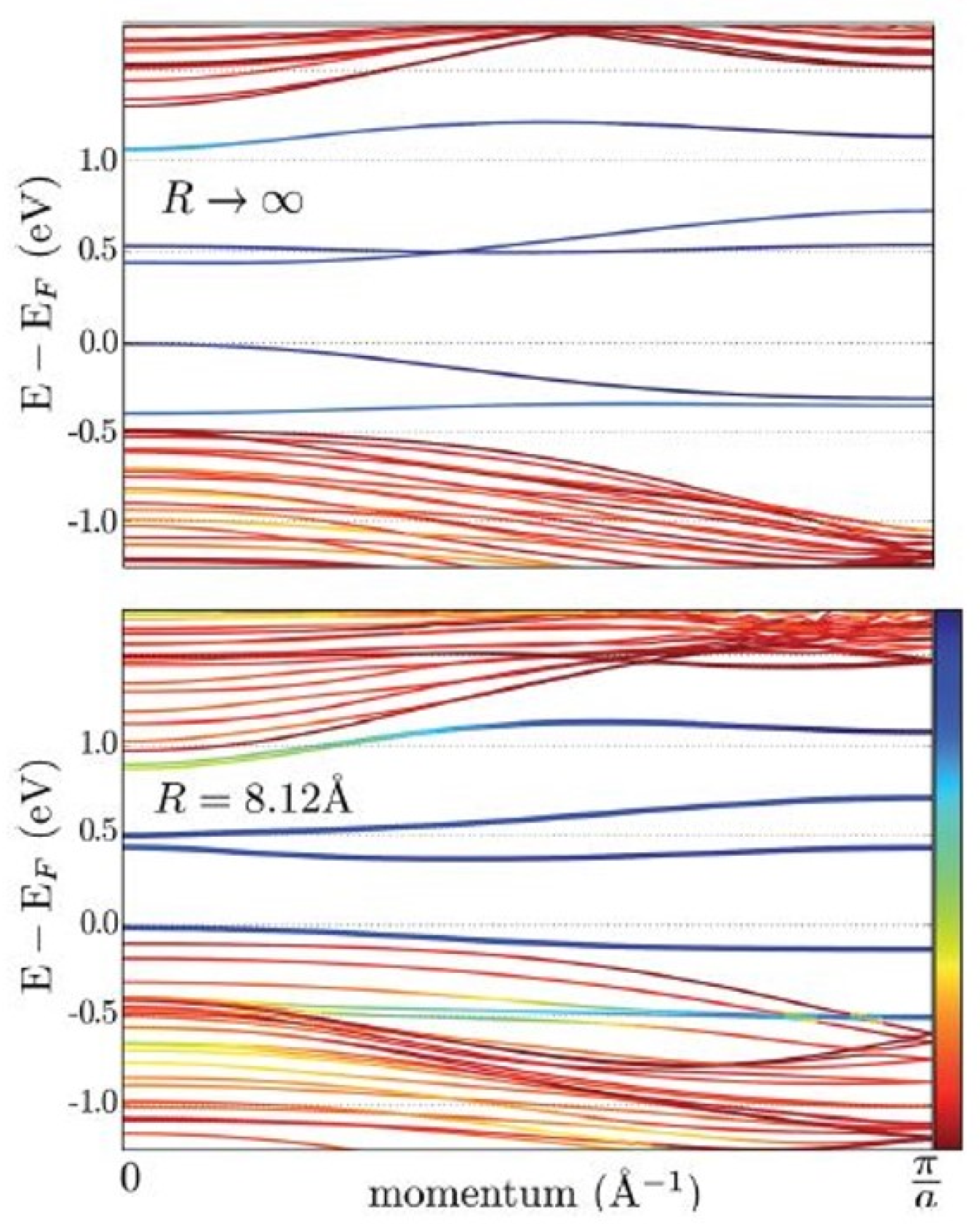
2. Curvature Engineering on 2D-Layered TMDs

The sphere diameter engineering (SDE) technique was demonstrated by Zeng et al. for manipulating the bandgap of 2D-layered materials [25]. By creating an isotropic curved surface, the strain of MoS2 crystals can be induced [25]. After the MoS2 growth processes via SDE, the liquid glass plane changes into a sphere having a specific diameter, resulting in a homogeneous and controllable lattice deformation of the supported 2D-layered materials with great precision and reliability. Moreover, the mass production of MoS2 with a specific bandgap can be fabricated by controlling the glass amount becoming the glass sphere. As compared to traditional strategies (i.e., unidirectional strain engineering), it is worth noting that the higher tuning performance of this approach owing to the lattice deformation of the MoS2 crystal is isotropic and multidirectional [18,32,33]. Moreover, this approach can obtain a uniform distribution of lattice deformation for all flakes on the entire isotropic sphere. The photoluminescence (PL) spectra of the MoS2 crystals grown on the glass spheres having different diameters show that a peak redshift of the neutral exciton can be detected with the decrease in the diameter of the sphere due to the electronic band structure tuning resulting from the lattice deformation increase of the monolayer MoS2 crystal [34]. By using this SDE strategy, the sphere design and assembly could boost the bandgap tuning of the post-growth MoS2 and maintain the uniform lattice deformation of 2D-layered crystals over the surface of the isotropic sphere. This technique opens avenues to tune the bandgap of low-dimensional nanomaterials (such as 2D-layered materials and nanowires) and help promote their practical applications [25].
In 2018, Gonz’alez et al. investigated the bending process of 2D-layered materials, which is related to external forces [35], and studied the bending of a MoS2 band in order to increase the complexity of the material, in this case, using the bending force on the central Mo layer while permitting the S atoms to move freely. As shown in Figure 1, the inner, bulk-like bands (the red lines) are qualitatively similar for R = 8.12 Å and R→∞, but the band gap is ~0.8 eV smaller, indicating that it is possible to control the bandgap of a MoS2 nanosheet by bending it [35].
Developing effective catalysts can be achieved by controlling the surface structure on the atomic scale; it is well known that the edge sites of a MoS2 nanosheet are active for catalysis. Synthesizing a contiguous thin film consisting of highly ordered double-gyroid MoS2 crystals having nanoscale pores can efficiently expose the edge sites of MoS2. The high surface curvature of the mesoporous double-gyroid MoS2 exposing large edge sites could provide excellent electrocatalytic activity toward hydrogen evolution reaction (HER) [36]. The HER activity data (i.e., cyclic voltammograms) of double-gyroid MoS2 with Mo deposition times of 10 s, 20 s, and 1 min show that the increased surface area for samples deposited with longer deposition times is obvious when comparing the difference in capacitance current in the region of −0.1 to +0.4 V versus the reversible hydrogen electrode (RHE). The sample deposited for 1 min shows the greatest capacitance while the sample deposited for 10 s shows the smallest capacitance. Meanwhile, this double-gyroid MoS2 also exhibited potential HER performance as compared to traditionally noble metal catalysts, such as Pt [36].

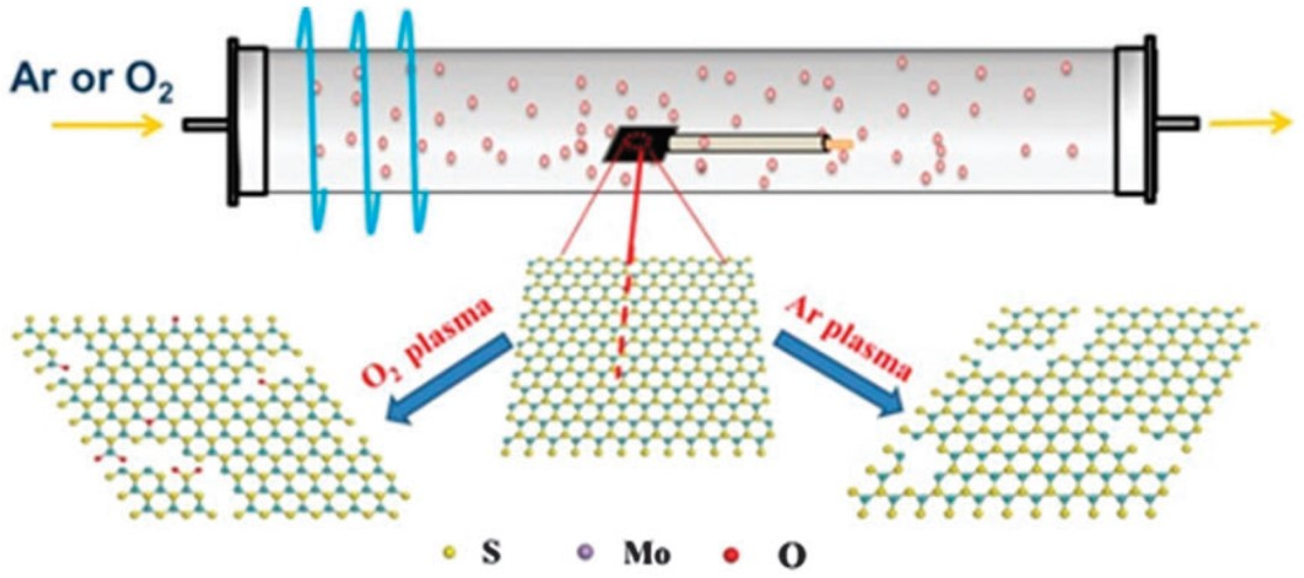
3. Plasma Treatment on 2D-Layered TMDs

A higher number of defects of pristine single-layer MoS2 could be created via oxygen plasma exposure and hydrogen treatment, resulting in a high density of exposed edges and an obvious enhancement in the hydrogen evolution activity [37]. In Figure 2a, the intensity of both A1g and E12g modes of single-layer MoS2 decreases with the oxygen plasma treatment time, indicating that the MoS2 lattice distortion is caused by oxygen plasma [38]. In addition, a new peak at 285 cm−1 (Mo−O bonds) becomes more obvious with the increase in the oxygen bombardment time [39]. Moreover, as shown in Figure 2b, the intensity of the PL peak (680 nm) also lowers with the increase in plasma treatment time, indicating that more defects and cracks were induced by the bombardment of oxygen [40,41]. Accordingly, oxygen plasma can not only decrease the MoS2 crystal symmetry but also increase the lattice distortion, inducing more defects in MoS2 for boosting electrochemical catalytic reactions. In Figure 3a, to reveal the effects of defects on the catalytic property of MoS2, the HER property characterization of the MoS2 monolayer with different oxygen plasma exposure times (0, 10, and 20 s) was measured. The sample (with 20 s oxygen plasma treatment) expresses the smallest onset potential, attributing to the largest amount of electrochemically active sites of MoS2 after plasma exposure. Moreover, a positive correlation exists between the enhancement of HER activity and the plasma exposure time after the correction of the j−V curve for iR losses via MoS2 itself. As shown in Figure 3b, the Tafel slope (~171 mV dec−1) of MoS2 with 20 s plasma treatment obviously decreases, indicating that the defects in the single-layer MoS2 basal plane can be induced effectively by oxygen plasma exposure for boosting HER [37].
In 2019, Nguyen et al. reported that the active sites can be effectively induced within the continuous MoS2 sheets by plasma treatment [42]. Maximum active sites in large-area single-layer MoS2 were obtained via N2 plasma to meet the requirement of a high HER performance. In order to reveal the effect of N2 plasma on the optical characteristics of MoS2, the Raman and PL spectroscopy are shown in Figure 4. The Raman peak (E2g and A1g) intensity and width of MoS2 decrease a lot and become broadened, respectively, implying that a lot of lattice distortion and defects (such as cracks and sulfur vacancies) generated after plasma treatment [37]. On the other hand, the PL intensity also rapidly decreased with plasma treatment time, attributing to more defects site induced by N2 plasma. For the HER performance, the MoS2 without plasma treatment showed relatively low HER activities with an onset potential at −460 mV (vs. reversible hydrogen electrode (RHE)). By contrast, the samples with N2 plasma treatment for 10–30 min showed a considerable decrease in the onset potential. The smallest value of the onset potential (−210 mV) was exhibited by the 20 min plasma-treated MoS2, as shown in Figure 5. Although this method is simple and controllable to maximize the HER efficiency of the wafer-scale MoS2, the plasma treatment time should still be carefully controlled for optimizing the active site. This method holds promise for further improving the HER efficiency of 2D-layered TMDS [42].
Tao et al. reported that the electrocatalytic activity of MoS2 thin-films for the HER significantly enhanced after using Ar or O2 plasma treatment [43]. Figure 6 illustrates the processes of O2 or Ar plasma treatment. With different Ar or O2 plasma treatment durations, the electronic properties and defect sites of MoS2 thin films could be adjusted. The polarization curves of the MoS2 thin films before and after plasma treatment are shown in Figure 7a,b. To compare with the pristine MoS2, the Ar and O2 plasma-treated MoS2 thin films show higher HER performance. At the beginning, the HER performance of MoS2 was improved with increasing Ar plasma treatment time due to the increase in defects. After Ar plasma treatment for 720 s, the MoS2 exhibited the best HER activity (a current density of 16.3 mA cm−2 at −350 mV). However, the HER activity sharply declined (11.83 mA cm−2) with increasing Ar plasma treatment time to 960 s, owing to the decrease in active species for too long a plasma treatment process. Furthermore, MoS2 with O2 plasma treatment showed a similar behavior of the HER activity. After 480 s O2 plasma treatment, the maximum HER activity of MoS2 was obtained. The HER activity decreased from 480 to 720 s plasma treatment, resulting from over-doping oxygen species, and the active species decreased for long-term plasma treatment. This report demonstrated that electrocatalytic activity on the 2D-layered material surface could be modified by controlling the plasma irradiation time [43]; however, over oxidation of MoS2 could probably cause negative effects on the device performance due to the decreases in active species. Moreover, it is well known that the formation of molybdenum oxides could also decrease the carrier mobility in pertinent electronic devices and result in the poor stability in acidic or alkaline electrolytes of the electrolysis system.

4. Heteroatom-Doping on 2D-Layered TMDs

Shi et al. proposed a strategy to enhance the HER performance of MoS2 by direct transition-metal doping [27]. The HER active centers of MoS2 come from the edge deformed sites, as everyone knows [37]. Therefore, to enhance the HER catalytic activity of MoS2, the effect of Zn atom doping on HER was investigated. The Raman spectrum of Zn-MoS2 and the pure MoS2 show a similar curve, as shown in Figure 8, indicating that there is no change in the MoS2 layered feature of Zn-MoS2. In other words, the physical characterizations show the high uniformity of Zn atom doping in the MoS2 structure. As shown in Figure 9a (green line), the bulk MoS2 shows poor HER activity (Tafel slope of 692 mV dec−1) as in the previous report, owing to huge lateral resistance. To compare with pure MoS2, Zn-MoS2 exhibits superior electrocatalytic activity for HER, as shown in Figure 9a, promising to reduce the gap with the commercial Pt/C catalyst (Figure 9a, blue line). For the long-term stability test, the profile for the cathodic wave after 1000 cyclic potential sweeps shows a similar current density with the initial curve, as shown in Figure 9b, indicating the ultra-high stability of Zn-MoS2 for HER. This low-cost strategy was demonstrated to design highly efficient electrocatalysts for HER, holding promise for broad applications in other catalytic systems [27].
In 2015, Deng et al. reported that the in-plane S atom catalytic activity of MoS2 can be activated with single-atom metal doping. As shown in Figure 10a, compared to the blank glassy carbon (GC) electrode and bulk MoS2, the pure few-layer MoS2 nanosheets (FL-MoS2) without Pt atom doping showed a higher activity [44]. However, the activity of FL-MoS2 without Pt atom doping was still much lower than with the 40% Pt/C catalyst. There is a big difference in the Tafel value of Pt–MoS2 (96 mV dec−1) and of the Pt/C electrocatalyst (32 mV dec−1), as shown in Figure 10b, implying that the mechanism should be low relative to Pt. By contrast, the Tafel value of Pt–MoS2 is closer to FL-MoS2 (98 mV dec−1). This result implies that the active sites of HER should also come from the S atoms rather than the Pt atoms in the Pt–MoS2 sample. For stability testing, the Pt-MoS2 catalyst exhibited a very stable performance after 5000 cycles of cyclic voltammetry (CV) scans, as shown in Figure 10c [44].
Wang and his group predicted the trends in HER activity of MoS2 structures with different transition metals (Co, Fe, Ni, Cu) doping via a computational descriptor-based approach [45]. The enhancement in HER incorporating transition metal doping into the edge sites of the vertically aligned MoS2 nanofilms was confirmed experimentally. Their polarization curves shows that Fe, Co, Ni, and Cu-doped MoS2 nanofilms achieve −2.3, −3.5, −2.4, and −2.6 mA cm−2 at the overpotential of 300 mV, respectively, around four times that of the pristine MoS2 (−0.6 mA cm−2 at 300 mV), indicating the large enhancement after the transition metal atoms incorporated into the edge sites. The Tafel plots corresponding to the above polarization plots suggest that the difference in Tafel slopes of pristine MoS2 (118 mV dec1) and MoS2 with doping (from 117 to 103 mV dec−1) results is very small, indicating that the rate-limiting step is not changed after the doping process. These results show that MoS2 could be doped with various transition metal dopants to discover new MoS2-based catalysts in the future [45].

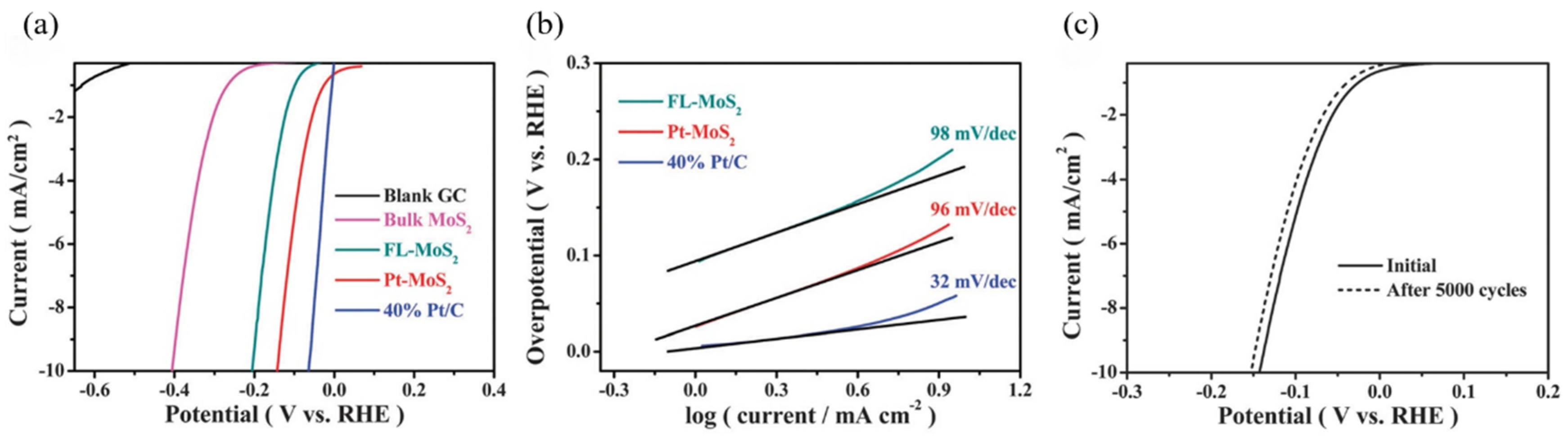
5. Surface Modification on 2D-Layered TMDs

Huang et al. reported that a composite film of molybdenum diselenide nanosheets (MoSe2 NSs)/poly(3,4-ethylenedioxythiophene):poly(styrenesulfonate) (PEDOT:PSS) was fabricated using a low-cost drop-coating method for the counter electrode (CE) of a dye-sensitized solar cell (DSSC) [46]. The morphological features of various CEs are shown in Figure 11. The smoothest morphology of the bare PEDOT:PSS film is shown in Figure 11a. However, the smooth surface could lead to few electrocatalytic active sites and poor electrochemical surface. Compared with the bare PEDOT:PSS film, the composite films of MP-1.00 (MoSe2 NSs in the PEDOT:PSS matrix) show rougher surfaces, as shown in Figure 11b. As shown in Figure 11c, the surface roughness of MoSe2 NSs (planar size: 100–800 nm; thickness: 10–50 nm) in the bare MoSe2 film is high. However, the poor adhesion of MoSe2 NSs in the bare MoSe2 film hinders electrocatalytic applications. With the incorporation of PEDOT:PSS, the composite films of MoSe2/PEDOT:PSS would exhibit better electrocatalytic activity as compared to the bare MoSe2 film; besides, the PEDOT:PSS could act as a binder to enhance the adhesion on the substrate, which could greatly improve the electro-catalytic ability and mechanic stability. Figure 12 shows the j–V curves of the DSSCs with the CEs of Pt, bare PEDOT:PSS, MP-1.00, and bare MoSe2. The pertinent photovoltaic parameters are listed in Table 1. The power conversion efficiency (η) of the DSSC with a composite film having equal weights of MoSe2 and PEDOT:PSS (MP-1.00) is 7.58 ± 0.05%, which is competitive with the efficiency of a Pt CE (7.81 ± 0.03%) [46].
Zhang et al. reported that the decoration of isolated Ni atoms on the surface of MoS2 NSs supported on multichannel carbon matrix (MCM) nanofibers can improve the hydrogen evolution activity obviously [31]. As shown in Figure 13a, the hierarchical shell composed of randomly assembled ultrathin MoS2 NSs can be clearly observed from the SEM image. There are no obvious changes in the original morphology of MCM@MoS2 after the modification of the Ni atom (Figure 13b). In addition, the cross-sectional image of the multichannel structure of the MCM@MoS2–Ni is shown in Figure 13c. As shown in Figure 14, compared with the original MoS2 (−297 mV), MCM @ MoS2 has a positively shifted overpotential at −10 mA cm−2 (−263 mV), showing a significantly enhanced performance. Moreover, hydrogen evolution is considerably accelerated by the MCM@MoS2–Ni catalyst, and it shows a smaller onset overpotential (−53 mV) and higher current increase rate. This report represents a good method to activate the electrocatalytic activity of MoS2 inert surfaces, which can be used in HER and other energy-related catalytic processes [31].

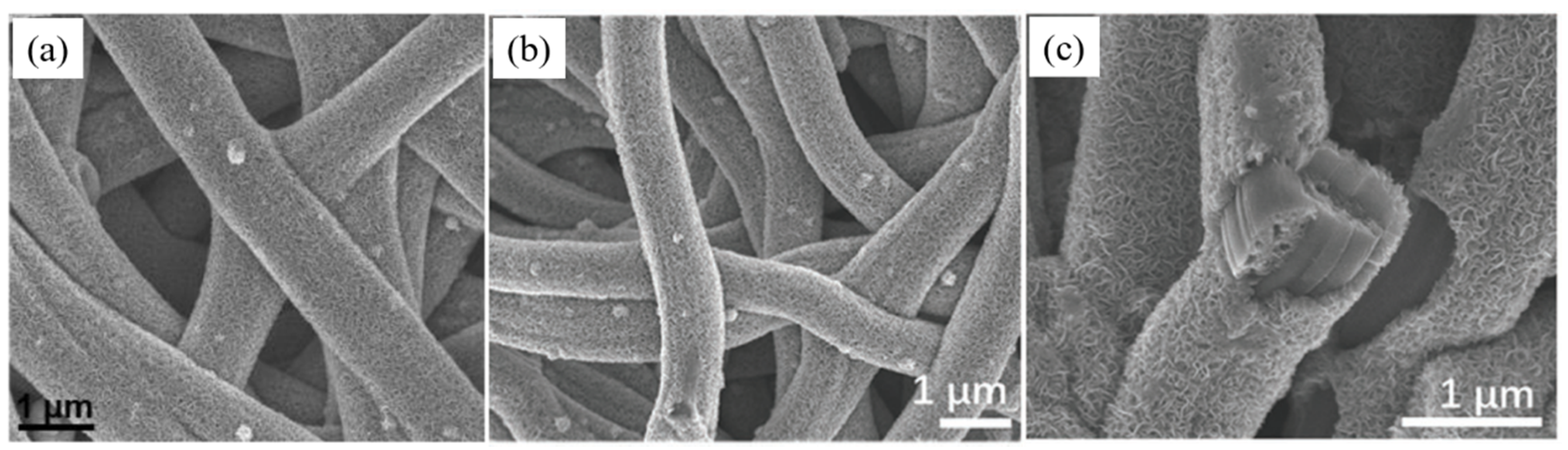
6. Edge Site Formation on 2D-Layered TMDs

In 2013, Xie et al. proposed creating active edge sites on the MoS2 surface by the defect engineering for enhancing HER performance [30]. As shown in Figure 15, by designing a reaction with a high concentration of precursors and different amounts of thiourea, the modulation of defects on the surface of MoS2 ultrathin NSs could be accomplished. As shown in Figure 16, the defect-rich MoS2 ultrathin NSs showed a small onset potential of 120 mV, and a fast-rising current under higher negative potential. Compared with the highly crystalline samples (160–250 mV) and the nanostructured MoS2, the defect-rich MoS2 ultrathin NSs exhibited a good catalytic activity owing to the unique defect-rich structure, resulting in more active edge sites [36,47] By contrast, polarization curves of defect-free MoS2 NSs and calcined MoS2 NSs showed not only poor HER performance with high onset potential (180 and 230 mV) but also low cathodic current density. In addition, although the onset overpotential of the thicker NSs is competitive with the defect-rich MoS2 ultrathin NSs, the cathodic current density is still unsatisfactory due to the limitation of the exposure of defect-induced active sites by assembly morphology. Therefore, the HER performance could be boosted significantly by the rich defects in the ultrathin NSs. As shown in Table 2, the defect-rich MoS2 ultra-thin NSs show the highest active site density, proving the primary enrichment effect of active edge sites resulting from rich defects. Furthermore, the NS structure could produce more available defect-induced edge sites owing to the higher surface area of the ultrathin NSs. Generally speaking, the great electrocatalytic behavior of the defect-rich MoS2 ultrathin NSs is attributed to the enrichment effect of active edge sites induced by abundant defects and the synergic effect of ultrathin NS morphology. This study demonstrates controllable defect engineering in MoS2 ultrathin NSs and opens avenues to develop other 2D-layered electrocatalysts (such as WS2 and MoSe2) [30].
Zhang et al. reported that the defect-rich MoS2 monolayer with the two-dimensional reticulated structure was facilely prepared by a conventional hydrothermal method (surfactant ethyl xanthate (C2H5OC(=S)SNa) as sulfur source). To enhance electronic and photoelectric properties, the inert basal plane and delivered active sites in the MoS2 monolayer should be triggered by increasing defects [48]. Figure 17 shows the Raman spectra of as-prepared MoS2 (i.e., defect-rich MoS2) and bulk MoS2. The E12g/A1g peaks of defect-rich MoS2 and bulk MoS2 are at ∼380.7/406.1 and∼383.0/408.5 cm−1, respectively. Compared to bulk MoS2, the Raman peaks of defect-rich MoS2 blue-shift, possibly owing to the vacancies in its structure [49]. Furthermore, the broader and weaker Raman peaks of the defect-rich MoS2 than bulk MoS2 imply its weak crystalline and abundant defects in its basal plane [50,51,52]. The S 2p3/2 XPS spectra were deconvolved into two components, as shown in Table 3. The peaks at ∼161.33 and ∼162.75 eV correspond to the full-bonded S atoms of the MoS2 monolayer and the part-coordinated S atoms, respectively [53,54,55]. Additionally, the atomic proportion of part-coordinated S atoms is 23.86%, estimating a lot of S vacancies in defect-rich MoS2. There are two characteristic bands of Mo 3d5/2 XPS at around 228.60 and 229.06 eV with a proportion of 57.90% and 42.10%, respectively, as shown in Table 3 [56]. The low band (228.60 eV) and the high band (229.06 eV) might be related to the Mo atoms with dangling bonds (lower valence than the full-coordinated Mo+4 atoms) and the full-coordinated Mo atoms of MoS2, respectively. Therefore, in addition to S vacancies, a lot of Mo vacancies exist in the defect-rich MoS2. The HER activity of the defect-rich MoS2 was measured by the electrochemical technique, as shown in Figure 18. The linear sweep voltammetry (LSV) curves in Figure 18a show the hydrogen evolution potentials of the defect-rich (235 mV) and bulk MoS2 (707 mV), respectively. In order to reach the 10 mA cm−2 current densities (j), the overpotentials (η) for the defect-rich and bulk MoS2 should reach 244.18 mV with a 58 mV dec−1 Tafel slope and 736.21 mV with a 173.6 mV dec−1 Tafel slope, respectively, as shown in Figure 18b [57,58], indicating the superior catalytic activity and hydrogen evolution velocity of the defect-rich MoS2. The electrochemical double-layer capacitance (Cdl) represents the active site quantities in the electrode interface, as shown in Figure 18c [59]. The larger Cdl value and very small Rct value of the defect-rich MoS2 imply the higher density of HER sites and high conductivity, respectively, possibly leading to the fast electron transfer and high-efficiency electrocatalytic process, as shown in Figure 18d [60]. The LSV curve for the initial cycle and that after 1000 CV cycles in Figure 18e showed similar results, implying the excellent stability of the defect-rich MoS2 material. All above results reveal that the defect-rich MoS2 possessed an excellent and stable activity for HER [48].

7. Conclusions and Outlook

2D-layered TMDs possess promising catalysis properties and have been widely investigated for the applications on electrochemical energy. Especially, research on hydrogen evolution is theoretically well supported that 2D-layered MoS2 exhibits much more favorable reaction coordinates for hydrogen evolution than most Pt-free catalysts [61]. In practically, though their basal plane shows poor activity toward catalysis reaction, several approaches, such as curvature engineering, plasma treatment, heteroatom-doping, edge site formation, and surface modification via nano-sized catalyst decoration, can be utilized to improve their catalysis activity efficiently. Future development of 2D-layered TMDs having superior catalytic activity would focus on the structural and interfacial engineering on 2D-layered TMDs. For example, the structural transformation of layered TMDs from a 2D sheet to 3D hollow sphere consisted of curved 2D TMDs, which could significantly increase the specific surface area and strain-induced active sites, as well as prevent the stacking and aggregation of most 2D-layered materials. Moreover, heteroatom-doping (e.g., single-atom doping or dual-atom co-doping) on curved 2D-layered materials is also theoretically demonstrated as a potential approach to further enhance the catalysis performance [62].

Author Contributions

Conceptualization and organization, C.-P.L. and D.-S.T.; Writing—original draft, C.-A.C., C.-L.L., and P.-K.Y. All authors have read and agreed to the published version of the manuscript.

Funding

This research received funding from Ministry of Science and Technology (MOST) of Taiwan.

Acknowledgments

This work was supported by the Ministry of Science and Technology (MOST) of Taiwan, under grant numbers 107-2113-M-845-001-MY3 and 109-2112-M-033-010-MY3.

Conflicts of Interest

The authors declare no conflict of interest.

References

  1. Dean, C.R.; Young, A.F.; Meric, I.; Lee, C.; Wang, L.; Sorgenfrei, S.; Watanabe, K.; Taniguchi, T.; Kim, P.; Shepard, K.L.; et al. Boron nitride substrates for high-quality graphene electronics. Nat. Nanotechnol. 2010, 5, 722–726. [Google Scholar] [CrossRef] [PubMed]
  2. Novoselov, K.S.; Geim, A.K.; Morozov, S.V.; Jiang, D.; Zhang, Y.; Dubonos, S.V.; Grigorieva, I.V.; Firsov, A.A. Electric field effect in atomically thin carbon films. Science 2004, 306, 666–669. [Google Scholar] [CrossRef] [PubMed] [Green Version]
  3. Tseng, C.-A.; Chen, C.-C.; Ulaganathan, R.K.; Lee, C.-P.; Chiang, H.-C.; Chang, C.-F.; Chen, Y.-T. One-step synthesis of antioxidative graphene-wrapped copper nanoparticles on flexible substrates for electronic and electrocatalytic applications. ACS Appl. Mater. Interfaces 2017, 9, 25067–25072. [Google Scholar] [CrossRef] [PubMed]
  4. Tseng, C.-A.; Lee, C.-P.; Huang, Y.-J.; Pang, H.-W.; Ho, K.-C.; Chen, Y.-T. One-step synthesis of graphene hollow nanoballs with various nitrogen-doped states for electrocatalysis in dye-sensitized solar cells. Mater. Today Energy 2018, 8, 15–21. [Google Scholar] [CrossRef]
  5. Tseng, C.-A.; Sahoo, P.K.; Lee, C.-P.; Lin, Y.-T.; Xu, J.-H.; Chen, Y.-T. Synthesis of CoO-decorated graphene hollow nanoballs for high-performance flexible supercapacitors. ACS Appl. Mater. Interfaces 2020, 12, 40426–40432. [Google Scholar] [CrossRef]
  6. Osada, M.; Sasaki, T. Two-dimensional dielectric nanosheets: Novel nanoelectronics from nanocrystal building blocks. Adv. Mater. 2012, 24, 210–228. [Google Scholar] [CrossRef]
  7. Pacilé, D.; Meyer, J.C.; Girit, Ç.Ö.; Zettl, A. The two-dimensional phase of boron nitride: Few-atomic-layer sheets and suspended membranes. Appl. Phys. Lett. 2008, 92, 133107. [Google Scholar] [CrossRef]
  8. Mishra, A.K.; Lakshmi, K.V.; Huang, L. Eco-friendly synthesis of metal dichalcogenides nanosheets and their environmental remediation potential driven by visible light. Sci. Rep. 2015, 5, 15718. [Google Scholar] [CrossRef] [Green Version]
  9. Ding, Y.; Wang, Y.; Ni, J.; Shi, L.; Shi, S.; Tang, W. First principles study of structural, vibrational and electronic properties of graphene-like MX2 (M=Mo, Nb, W, Ta; X=S, Se, Te) monolayers. Phys. B Condens. Matter 2011, 406, 2254–2260. [Google Scholar] [CrossRef]
  10. Zhang, X.; Qiao, X.-F.; Shi, W.; Wu, J.-B.; Jiang, D.-S.; Tan, P.-H. Phonon and Raman scattering of two-dimensional transition metal dichalcogenides from monolayer, multilayer to bulk material. Chem. Soc. Rev. 2015, 44, 2757–2785. [Google Scholar] [CrossRef] [Green Version]
  11. Ayari, A.; Cobas, E.; Ogundadegbe, O.; Fuhrer, M.S. Realization and electrical characterization of ultrathin crystals of layered transition-metal dichalcogenides. J. Appl. Phys. 2007, 101, 014507. [Google Scholar] [CrossRef] [Green Version]
  12. Tran, P.D.; Wong, L.H.; Barber, J.; Loo, J.S.C. Recent advances in hybrid photocatalysts for solar fuel production. Energy Environ. Sci. 2012, 5, 5902. [Google Scholar] [CrossRef]
  13. Han, S.A.; Bhatia, R.; Kim, S.-W. Synthesis, properties and potential applications of two-dimensional transition metal dichalcogenides. Nano Converg. 2015, 2, 17. [Google Scholar] [CrossRef] [Green Version]
  14. Zhang, C.; Gong, C.; Nie, Y.; Min, K.-A.; Liang, C.; Oh, Y.J.; Zhang, H.; Wang, W.; Hong, S.; Colombo, L.; et al. Systematic study of electronic structure and band alignment of monolayer transition metal dichalcogenides in Van der Waals heterostructures. 2D Mater. 2016, 4, 015026. [Google Scholar] [CrossRef]
  15. Chhowalla, M.; Shin, H.S.; Eda, G.; Li, L.-J.; Loh, K.P.; Zhang, H. The chemistry of two-dimensional layered transition metal dichalcogenide nanosheets. Nat. Chem. 2013, 5, 263–275. [Google Scholar] [CrossRef] [PubMed]
  16. Pan, H. Metal dichalcogenides monolayers: Novel catalysts for electrochemical hydrogen production. Sci. Rep. 2014, 4, 5348. [Google Scholar] [CrossRef] [PubMed] [Green Version]
  17. Velusamy, D.B.; Kim, R.H.; Cha, S.; Huh, J.; Khazaeinezhad, R.; Kassani, S.H.; Song, G.; Cho, S.M.; Cho, S.H.; Hwang, I.; et al. Flexible transition metal dichalcogenide nanosheets for band-selective photodetection. Nat. Commun. 2015, 6, 8063. [Google Scholar] [CrossRef] [Green Version]
  18. Conley, H.J.; Wang, B.; Ziegler, J.I.; Haglund, R.F., Jr.; Pantelides, S.T.; Bolotin, K.I. Bandgap engineering of strained monolayer and bilayer MoS2. Nano Lett. 2013, 13, 3626–3630. [Google Scholar] [CrossRef] [Green Version]
  19. Dumcenco, D.; Ovchinnikov, D.; Lopez Sanchez, O.; Gillet, P.; Alexander, D.T.L.; Lazar, S.; Radenovic, A.; Kis, A. Large-area MoS2 grown using H2S as the sulphur source. 2d Mater. 2015, 2, 4. [Google Scholar] [CrossRef]
  20. Xu, J.; Zhang, J.; Zhang, W.; Lee, C.-S. Interlayer nanoarchitectonics of two-dimensional transition-metal dichalcogenides nanosheets for energy storage and conversion applications. Adv. Energy Mater. 2017, 7, 1700571. [Google Scholar] [CrossRef] [Green Version]
  21. Voiry, D.; Goswami, A.; Kappera, R.; Silva, C.; Kaplan, D.; Fujita, T.; Chen, M.; Asefa, T.; Chhowalla, M. Covalent functionalization of monolayered transition metal dichalcogenides by phase engineering. Nat. Chem. 2015, 7, 45–49. [Google Scholar] [CrossRef] [PubMed]
  22. Kim, S.J.; Kim, D.W.; Lim, J.; Cho, S.Y.; Kim, S.O.; Jung, H.T. Large-area buckled MoS2 films on the graphene substrate. ACS Appl. Mater. Interfaces 2016, 8, 13512–13519. [Google Scholar] [CrossRef] [PubMed]
  23. Bissett, M.A.; Tsuji, M.; Ago, H. Strain engineering the properties of graphene and other two-dimensional crystals. Phys. Chem. Chem. Phys. 2014, 16, 11124–11138. [Google Scholar] [CrossRef]
  24. Desai, S.B.; Seol, G.; Kang, J.S.; Fang, H.; Battaglia, C.; Kapadia, R.; Ager, J.W.; Guo, J.; Javey, A. Strain-induced indirect to direct bandgap transition in multilayer WSe2. Nano Lett. 2014, 14, 4592–4597. [Google Scholar] [CrossRef] [PubMed]
  25. Zeng, M.; Liu, J.; Zhou, L.; Mendes, R.G.; Dong, Y.; Zhang, M.-Y.; Cui, Z.-H.; Cai, Z.; Zhang, Z.; Zhu, D.; et al. Bandgap tuning of two-dimensional materials by sphere diameter engineering. Nat. Mater. 2020, 19, 528–533. [Google Scholar] [CrossRef]
  26. Azcatl, A.; Qin, X.; Prakash, A.; Zhang, C.; Cheng, L.; Wang, Q.; Lu, N.; Kim, M.J.; Kim, J.; Cho, K.; et al. Covalent nitrogen doping and compressive strain in MoS2 by remote N2 plasma exposure. Nano Lett. 2016, 16, 5437–5443. [Google Scholar] [CrossRef] [Green Version]
  27. Shi, Y.; Zhou, Y.; Yang, D.-R.; Xu, W.-X.; Wang, C.; Wang, F.-B.; Xu, J.-J.; Xia, X.-H.; Chen, H.-Y. Energy level engineering of MoS2 by transition-metal doping for accelerating hydrogen evolution reaction. J. Am. Chem. Soc. 2017, 139, 15479–15485. [Google Scholar] [CrossRef]
  28. Kong, D.; Wang, H.; Cha, J.J.; Pasta, M.; Koski, K.J.; Yao, J.; Cui, Y. Synthesis of MoS2 and MoSe2 films with vertically aligned layers. Nano Lett. 2013, 13, 1341–1347. [Google Scholar] [CrossRef]
  29. Padmajan Sasikala, S.; Singh, Y.; Bing, L.; Yun, T.; Koo, S.H.; Jung, Y.; Kim, S.O. Longitudinal unzipping of 2D transition metal dichalcogenides. Nat. Commun. 2020, 11, 5032. [Google Scholar] [CrossRef]
  30. Xie, J.; Zhang, H.; Li, S.; Wang, R.; Sun, X.; Zhou, M.; Zhou, J.; Lou, X.; Xie, Y. Defect-rich MoS2 ultrathin nanosheets with additional active edge sites for enhanced electrocatalytic hydrogen evolution. Adv. Mater. 2013, 25. [Google Scholar] [CrossRef]
  31. Zhang, H.; Yu, L.; Chen, T.; Zhou, W.; Lou, X.W. Surface Modulation of hierarchical MoS2 nanosheets by Ni single atoms for enhanced electrocatalytic hydrogen evolution. Adv. Funct. Mater. 2018, 28. [Google Scholar] [CrossRef]
  32. He, K.; Poole, C.; Mak, K.F.; Shan, J. Experimental demonstration of continuous electronic structure tuning via strain in atomically thin MoS2. Nano Lett. 2013, 13, 2931–2936. [Google Scholar] [CrossRef] [PubMed] [Green Version]
  33. Zhu, C.R.; Wang, G.; Liu, B.L.; Marie, X.; Qiao, X.F.; Zhang, X.; Wu, X.X.; Fan, H.; Tan, P.H.; Amand, T.; et al. Strain tuning of optical emission energy and polarization in monolayer and bilayer MoS2. Phys. Rev. B 2013, 88, 121301. [Google Scholar] [CrossRef] [Green Version]
  34. Feng, J.; Qian, X.; Huang, C.-W.; Li, J. Strain-engineered artificial atom as a broad-spectrum solar energy funnel. Nat. Photonics 2012, 6, 866–872. [Google Scholar] [CrossRef]
  35. González, R.I.; Valencia, F.J.; Rogan, J.; Valdivia, J.A.; Sofo, J.; Kiwi, M.; Munoz, F. Bending energy of 2D materials: Graphene, MoS2 and imogolite. RSC Adv. 2018, 8, 4577–4583. [Google Scholar] [CrossRef] [Green Version]
  36. Kibsgaard, J.; Chen, Z.; Reinecke, B.N.; Jaramillo, T.F. Engineering the surface structure of MoS2 to preferentially expose active edge sites for electrocatalysis. Nat. Mater. 2012, 11, 963–969. [Google Scholar] [CrossRef]
  37. Ye, G.; Gong, Y.; Lin, J.; Li, B.; He, Y.; Pantelides, S.T.; Zhou, W.; Vajtai, R.; Ajayan, P.M. Defects engineered monolayer MoS2 for improved hydrogen evolution reaction. Nano Lett. 2016, 16, 1097–1103. [Google Scholar] [CrossRef]
  38. Kang, N.; Paudel, H.P.; Leuenberger, M.N.; Tetard, L.; Khondaker, S.I. Photoluminescence quenching in single-layer MoS2 via oxygen plasma treatment. J. Phys. Chem. C 2014, 118, 21258–21263. [Google Scholar] [CrossRef] [Green Version]
  39. Nan, H.; Wang, Z.; Wang, W.; Liang, Z.; Lu, Y.; Chen, Q.; He, D.; Tan, P.; Miao, F.; Wang, X.; et al. Strong photoluminescence enhancement of MoS2 through defect engineering and oxygen bonding. ACS Nano 2014, 8, 5738–5745. [Google Scholar] [CrossRef] [Green Version]
  40. Yang, J.; Kim, S.; Choi, W.; Park, S.H.; Jung, Y.; Cho, M.-H.; Kim, H. Improved growth behavior of atomic-layer-deposited high-k dielectrics on multilayer MoS2 by oxygen plasma pretreatment. ACS Appl. Mater. Interfaces 2013, 5, 4739–4744. [Google Scholar] [CrossRef]
  41. Islam, M.R.; Kang, N.; Bhanu, U.; Paudel, H.P.; Erementchouk, M.; Tetard, L.; Leuenberger, M.N.; Khondaker, S.I. Tuning the electrical property via defect engineering of single layer MoS2 by oxygen plasma. Nanoscale 2014, 6, 10033–10039. [Google Scholar] [CrossRef] [PubMed] [Green Version]
  42. Nguyen, A.D.; Nguyen, T.K.; Le, C.T.; Kim, S.; Ullah, F.; Lee, Y.; Lee, S.; Kim, K.; Lee, D.; Park, S.; et al. Nitrogen-Plasma-Treated Continuous Monolayer MoS2 for Improving Hydrogen Evolution Reaction. ACS Omega 2019, 4, 21509–21515. [Google Scholar] [CrossRef] [PubMed] [Green Version]
  43. Tao, L.; Duan, X.; Wang, C.; Duan, X.; Wang, S. Plasma-engineered MoS2 thin-film as an efficient electrocatalyst for hydrogen evolution reaction. Chem. Commun. 2015, 51, 7470–7473. [Google Scholar] [CrossRef] [PubMed]
  44. Deng, J.; Li, H.; Xiao, J.; Tu, Y.; Deng, D.; Yang, H.; Tian, H.; Li, J.; Ren, P.; Bao, X. Triggering the electrocatalytic hydrogen evolution activity of the inert two-dimensional MoS2 surface via single-atom metal doping. Energy Environ. Sci. 2015, 8, 1594–1601. [Google Scholar] [CrossRef]
  45. Wang, H.; Tsai, C.; Kong, D.; Chan, K.; Abild-Pedersen, F.; Nørskov, J.K.; Cui, Y. Transition-metal doped edge sites in vertically aligned MoS2 catalysts for enhanced hydrogen evolution. Nano Res. 2015, 8, 566–575. [Google Scholar] [CrossRef]
  46. Huang, Y.-J.; Fan, M.-S.; Li, C.-T.; Lee, C.-P.; Chen, T.-Y.; Vittal, R.; Ho, K.-C. MoSe2 nanosheet/poly(3,4-ethylenedioxythiophene): Poly(styrenesulfonate) composite film as a Pt-free counter electrode for dye-sensitized solar cells. Electrochim. Acta 2016, 211, 794–803. [Google Scholar] [CrossRef]
  47. Chen, Z.; Cummins, D.; Reinecke, B.N.; Clark, E.; Sunkara, M.K.; Jaramillo, T.F. Core-shell MoO3-MoS2 nanowires for hydrogen evolution: A functional design for electrocatalytic materials. Nano Lett. 2011, 11, 4168–4175. [Google Scholar] [CrossRef]
  48. Zhang, Z.; Dong, Y.; Sun, H.; Liu, G.; Liu, S.; Yang, X. Defect-rich 2D reticulated MoS2 monolayers: Facile hydrothermal preparation and marvellous photoelectric properties. J. Taiwan Inst. Chem. Eng. 2019, 101, 221–230. [Google Scholar] [CrossRef]
  49. Abinaya, R.; Archana, J.; Harish, S.; Navaneethan, M.; Ponnusamy, S.; Muthamizhchelvan, C.; Shimomura, M.; Hayakawa, Y. Ultrathin layered MoS2 nanosheets with rich active sites for enhanced visible light photocatalytic activity. RSC Adv. 2018, 8, 26664–26675. [Google Scholar] [CrossRef] [Green Version]
  50. Jiang, Y.; Wang, D.; Li, J.; Li, M.; Pan, Z.; Ma, H.; Lv, G.; Qu, W.; Wang, L.; Tian, Z. Designing MoS2 nanocatalysts with increased exposure of active edge sites for anthracene hydrogenation reaction. Catal. Sci. Technol. 2017, 7, 2998–3007. [Google Scholar] [CrossRef]
  51. Liu, K.-K.; Zhang, W.; Lee, Y.-H.; Lin, Y.-C.; Chang, M.-T.; Su, C.-Y.; Chang, C.-S.; Li, H.; Shi, Y.; Zhang, H.; et al. Growth of large-area and highly crystalline MoS2 thin layers on insulating substrates. Nano Lett. 2012, 12, 1538–1544. [Google Scholar] [CrossRef] [PubMed] [Green Version]
  52. Gogoi, G.; Arora, S.; Vinothkumar, N.; De, M.; Qureshi, M. Quaternary semiconductor Cu2ZnSnS4 loaded with MoS2 as a co-catalyst for enhanced photo-catalytic activity. RSC Adv. 2015, 5, 40475–40483. [Google Scholar] [CrossRef]
  53. Jong, A.D.; Borg, H.; Ijzendoorn, L.J.; Soudant, V.G.F.M.; Beer, V.D.; Veen, J.; Niemantsverdriet, J. Sulfidation mechanism of molybdenum catalysts supported on SiO2/Si(100) model support studied by surface spectroscopy. J. Phys. Chem. 1993, 97, 6477–6483. [Google Scholar] [CrossRef] [Green Version]
  54. Stevens, G.C.; Edmonds, T. Electron spectroscopy for chemical analysis spectra of molybdenum sulfides. J. Catal. 1975, 37, 544–547. [Google Scholar] [CrossRef]
  55. Benoist, L.; Gonbeau, D.; Pfister-Guillouzo, G.; Schmidt, E.; Meunier, G.; Levasseur, A. X-ray photoelectron spectroscopy characterization of amorphous molybdenum oxysulfide thin films. Thin Solid Film. 1995, 258, 110–114. [Google Scholar] [CrossRef]
  56. Shuxian, Z.; Hall, W.K.; Ertl, G.; Knözinger, H. X-ray photoemission study of oxygen and nitric oxide adsorption on MoS2. J. Catal. 1986, 100, 167–175. [Google Scholar] [CrossRef]
  57. Wu, H.B.; Xia, B.Y.; Yu, L.; Yu, X.-Y.; Lou, X.W. Porous molybdenum carbide nano-octahedrons synthesized via confined carburization in metal-organic frameworks for efficient hydrogen production. Nat. Commun. 2015, 6, 6512. [Google Scholar] [CrossRef]
  58. Zeng, M.; Li, Y. Recent advances in heterogeneous electrocatalysts for the hydrogen evolution reaction. J. Mater. Chem. A 2015, 3, 14942–14962. [Google Scholar] [CrossRef]
  59. Jian, W.; Cheng, X.; Huang, Y.; You, Y.; Zhou, R.; Sun, T.; Xu, J. Arrays of ZnO/MoS2 nanocables and MoS2 nanotubes with phase engineering for bifunctional photoelectrochemical and electrochemical water splitting. Chem. Eng. J. 2017, 328, 474–483. [Google Scholar] [CrossRef]
  60. Tian, J.; Liu, Q.; Cheng, N.; Asiri, A.M.; Sun, X. Self-supported Cu3P nanowire arrays as an integrated high-performance three-dimensional cathode for generating hydrogen from water. Angew. Chem. (Int. Ed. Engl.) 2014, 53, 9577–9581. [Google Scholar] [CrossRef]
  61. Hinnemann, B.; Moses, P.G.; Bonde, J.; Jørgensen, K.P.; Nielsen, J.H.; Horch, S.; Chorkendorff, I.; Nørskov, J.K. Biomimetic hydrogen evolution:  MoS2 nanoparticles as catalyst for hydrogen evolution. J. Am. Chem. Soc. 2005, 127, 5308–5309. [Google Scholar] [CrossRef] [PubMed]
  62. Qu, Y.; Ke, Y.; Shao, Y.; Chen, W.; Kwok, C.T.; Shi, X.; Pan, H. Effect of curvature on the hydrogen evolution reaction of graphene. J. Phys. Chem. C 2018, 122, 25331–25338. [Google Scholar] [CrossRef]
Figure 1. Band structure of a flat (upper panel) and a bent (lower panels) MoS2 nanoribbon [35]. The different color shows the location of the eigenvalues: The inner subbands (i.e., bulk-like) and the edge subbands are red and blue, respectively; the hybridization of bulk and edge states are between red and blue.
Catalysts 11 00151 g001
Figure 2. (a) Raman and (b) PL spectra of single-layer MoS2 show that the peak intensity and position decrease and shift, respectively, with different oxygen plasma exposure times [37].
Catalysts 11 00151 g002
Figure 3. Hydrogen evolution reaction (HER) properties of single-layer MoS2 with different oxygen plasma treatment times (0, 10, and 20 s). (a) Linear sweep voltammetry (LSV) curves show a positive correlation between the HER activity enhancement of single-layer MoS2 and the plasma exposure time at the cathodic sweep of the first cycle. (b) Tafel plots show the better performance in electrochemical activity of the single-layer MoS2 catalyst after 20 s oxygen plasma treatment [37].
Catalysts 11 00151 g003
Figure 4. (a) Raman and (b) PL characteristics of MoS2 with varying N2 plasma treatment time [42].
Catalysts 11 00151 g004
Figure 5. (a) iR-corrected linear sweep voltammograms and (b) Tafel plots with varying N2 plasma treatment time [42].
Catalysts 11 00151 g005
Figure 6. The development of defect sites in the MoS2 thin films after O2 or Ar plasma treatment [43].
Catalysts 11 00151 g006
Figure 7. The polarization curves of the MoS2 thin films at a 2 mV s−1 scan rate after different (a) Ar plasma and (b) O2 plasma treatment times [43].
Catalysts 11 00151 g007
Figure 8. Raman characteristics of pure MoS2 (black line) and Zn-MoS2 (red line) [27].
Catalysts 11 00151 g008
Figure 9. (a) Polarization curves of HER for bulk MoS2, Pt/C, pure MoS2, and Zn-MoS2. (b) The polarization stability tests of Zn-MoS2 catalyst (black line: Initial state; red line: After 1000 cycles) [27].
Catalysts 11 00151 g009
Figure 10. (a) HER polarization curves of Pt–MoS2, blank glassy carbon (GC) electrode, bulk MoS2, few-layer (FL)-MoS2, and 40% Pt/C, respectively. (b) Tafel plots of FL-MoS2 (98 mV dec−1), Pt–MoS2 (96 mV dec−1), and 40% Pt/C (32 mV dec−1). (c) The polarization stability tests of Pt–MoS2 between 0.13 and +0.57 V (vs. reversible hydrogen electrode (RHE)) at 100 mV s−1 (solid line: Initial state; broken line: After 5000 cycles of CV scans) [44].
Catalysts 11 00151 g010
Figure 11. FE-SEM images show the surface morphology of (a) bare PEDOT:PSS, (b) MP-1.00, and (c) bare MoSe2 [46].
Catalysts 11 00151 g011
Figure 12. J–V curves of the (dye-sensitized solar cell) DSSCs with Pt counter electrodes (CEs), bare PEDOT:PSS CEs, MP-1.00 CEs, and bare MoSe2 CEs [46].
Catalysts 11 00151 g012
Figure 13. FESEM images of the multichannel carbon matrix (MCM)@MoS2 nanofiber (a) without and (b) with Ni-atom modification. (c) The zoomed-in FESEM image of the hierarchical MCM@MoS2–Ni nanofiber [31].
Catalysts 11 00151 g013
Figure 14. LSV curves of MoS2 (blue line), MCM@MoS2 (black line), and MCM@MoS2-Ni (red line) in 0.5 m H2SO4 aqueous solution [31].
Catalysts 11 00151 g014
Figure 15. (a) Sketch of defect-free and defect-rich structures. (b) Synthetic processes of defect-free and defect-rich samples, respectively [30].
Catalysts 11 00151 g015
Figure 16. Polarization curves of various samples (defect-rich and defect-free MoS2, thicker nanosheet (NS), calcined MoS2, bulk MoS2, blank GC, and Pt) [30].
Catalysts 11 00151 g016
Figure 17. Raman characteristics of as-prepared (red line) and bulk MoS2 (blue line) [48].
Catalysts 11 00151 g017
Figure 18. (a) Polarization curves and (b) Tafel slopes of bulk MoS2 (blue line), as-prepared MoS2 monolayer (red line), and Pt (black line), respectively. (c) The double-layer capacitances Cdl of bulk MoS2 (blue line), as-prepared MoS2 monolayer (red line), (d) Nyquist diagrams of bulk MoS2 (blue square), as-prepared MoS2 monolayer (red dot) measured at 300 mV overpotential, and (e) the polarization durability test of the as-prepared MoS2 monolayer (red line: Initial state, blue line: After 1000 cycles) [48].
Catalysts 11 00151 g018
Table 1. Photovoltaic parameters (η (%), Voc (V), jsc (mA cm−2), and fill-factor (FF)) of the DSSCs with various CEs were measured at 100 mW cm−2 (AM 1.5G). The standard deviation data for each kind of DSSC were obtained from three cells with the same fabrication processes [46].
Counter Electrodeη (%)VOC (V)jSC (mA cm−2)FF
Pt7.81 ± 0.030.74 ± 0.0016.38 ± 0.030.65 ± 0.00
Bare PEDOT:PSS2.90 ± 0.030.67 ± 0.009.32 ± 0.250.46 ± 0.01
MP-0.256.28 ± 0.250.67 ± 0.0115.42 ± 0.550.61 ± 0.01
MP-0.506.67 ± 0.150.68 ± 0.0115.66 ± 0.290.61 ± 0.00
MP-1.007.58 ± 0.050.70 ± 0.0115.97 ± 0.180.67 ± 0.01
MP-2.006.08 ± 0.040.68 ± 0.0115.81 ± 0.210.57 ± 0.01
Bare MoSe22.29 ± 0.040.66 ± 0.0112.65 ± 0.310.28 ± 0.01
Table 2. HER parameters (number of active sites (10−3 mol g−1), turnover frequency (TOF) (s−1), Tafel slope (mV dec−1), Tafel region (mV), j0 (μA cm−2), and j (mA cm−2)) of various MoS2 samples [30].
Materials (a)Number of Active Sites [10−3 mol g−1]TOF [s−1] (b)Tafel Slope [mV dec−1]Tafel Region [mV]j0 [µA cm−2] (c)j [mA cm−2] (d)
Defect-rich ultrathin NSs1.7850.72550120–1808.9170.0
Defect-free ultrathin NSs0.6200.49687180–2403.1616.8
Calcined NSs0.3110.46790230–3005.628.2
Thicker NSs assembles0.5820.65388120–2507.9420.3
Bulk0.1370.30481250–3500.322.3
(a) All the parameters were measured under the same conditions, i.e., catalyst loading weight of 0.285 mg cm−2 on glassy carbon electrode in 0.5 M H2SO4 aqueous solution; (b) TOFs were measured at η = 300 mV; (c) exchanged current densities (j0) were obtained from Tafel curves by using extrapolation methods; (d) cathodic (j) was recorded at η = 300 mV.
Table 3. The S 2p and Mo 3d XPS peak parameters of the as-prepared MoS2 monolayer [48].
ElementsBinding Energy/eVFWHM c/eVAtomic Ratio/%Affiliation
S (2p)161.33/162.51 a1.2950.76/25.38S in MoS2
162.75/163.93 a1.3015.74/8.12Vacant S in MoS2
Mo (3d)228.60/231.74 b1.2525.61/16.49Mo in MoS2
229.06/232.39 b0.7435.09/22.81Vacant Mo in MoS2
a (S 2p3/2)/(S 2p1/2); b (Mo 3d5/2)/(Mo 3d3/2); c FWHM: Full-width at half-maximum.
Publisher’s Note: MDPI stays neutral with regard to jurisdictional claims in published maps and institutional affiliations.

