Article

TiO2-HfN Radial Nano-Heterojunction: A Hot Carrier Photoanode for Sunlight-Driven Water-Splitting

1
Department of Electrical and Computer Engineering, University of Alberta, Edmonton, AB T6G 1H9, Canada
2
Department of Chemical and Materials Engineering, University of Alberta, Edmonton, AB T6G 1H9, Canada
3
Nanotechnology Research Centre, National Research Council Canada, 11421 Saskatchewan Drive, Edmonton, AB T6G 2M9, Canada
*
Author to whom correspondence should be addressed.
Catalysts 2021, 11(11), 1374; https://doi.org/10.3390/catal11111374
Submission received: 25 October 2021 / Revised: 11 November 2021 / Accepted: 11 November 2021 / Published: 14 November 2021

Abstract

:
The lack of active, stable, earth-abundant, and visible-light absorbing materials to replace plasmonic noble metals is a critical obstacle for researchers in developing highly efficient and cost-effective photocatalytic systems. Herein, a core–shell nanotube catalyst was fabricated consisting of atomic layer deposited HfN shell and anodic TiO2 support layer with full-visible regime photoactivity for photoelectrochemical water splitting. The HfN active layer has two unique characteristics: (1) A large bandgap between optical and acoustic phonon modes and (2) No electronic bandgap, which allows a large population of long life-time hot carriers, which are used to enhance the photoelectrochemical performance. The photocurrent density (≈2.5 mA·cm−2 at 1 V vs. Ag/AgCl) obtained in this study under AM 1.5G 1 Sun illumination is unprecedented, as it is superior to most existing plasmonic noble metal-decorated catalysts and surprisingly indicates a photocurrent response that extends to 730 nm. The result demonstrates the far-reaching application potential of replacing active HER/HOR noble metals such as Au, Ag, Pt, Pd, etc. with low-cost plasmonic ceramics.

Graphical Abstract

1. Introduction

The group IV transition metal nitrides are beginning to attract a great deal of attention due to their unique characteristics such as exhibiting both metallic and semiconducting properties, possessing ceramic hardness, high thermal tolerance, and chemical resistance, showing the possibility for substitution of plasmonic noble metal, etc. [1,2]. Notwithstanding all the advantages, there have been rather few practical applications demonstrated. Most studies in the field have focused on material synthesis and characterization [3,4]. Among all the transition metal nitrides, titanium nitride is by far the most studied and utilized material [5,6,7], while hafnium nitride is basically unexplored and rarely utilized in optoelectronic devices. There are many reports investigating approaches to synthesize high-quality HfN. We are interested in employing HfN as a hot carrier absorber because its wide phonon gap can slow down the carrier thermalization process. Saha et al. calculated its electronic structure indicating its unique phonon dispersion of acoustic and optical branches [8]. Based on this feature, Chung et al. proposed using HfN in hot carrier solar cells and obtained a decay time of 1.7 ns in a transient absorption spectroscopic measurement [9]. The one and only catalytic application report was from Chiara et al., in which HfN nanoparticles were used for electrocatalytic oxygen evolution, and the highest performance was 10 mA·cm−2 at an overpotential of 358 mV [10]. Another similar work was presented by Yang et al. reporting electrocatalytic hydrogen evolution using nitrogen-plasma-treated hafnium oxyhydroxide [11]. Based on the findings from pioneer studies, HfN is worth investigating as a photocatalyst for solar energy conversion due to the following reasons: (1) high thermal and chemical resistance, and photochemical stability under harsh conditions; (2) long hot carrier lifetime; (3) plasmon resonance in the Vis-NIR regime; and (4) cost-efficient alternative to noble metals. Despite the aforementioned properties that are particularly beneficial to photocatalytic energy conversion, no one has reported the successful utilization of HfN for any kind of photocatalytic reactions. With this aim in mind, a photoanode consisting of TiO2(core)–HfN(shell) nanotube arrays (HfN-TNT) was deployed in photoelectrochemical water splitting and achieved a champion photocurrent of 2.48 mA·cm−2 under 1 Sun illumination (AM 1.5G) at an applied bias of +0.6 V vs. Ag/AgCl reference electrode in 1 M KOH solution. A photocurrent response of 2.39 mA·cm−2 during light on–off cycling was measured under identical conditions. To the best of our knowledge, this performance is superior to most plasmonic noble metal-decorated TiO2-based catalysts. The TiO2 nanotube array (core) was grown by electrochemical anodization of a Ti film sputtered at room temperature on a non-native fluorine-doped tin oxide (FTO)-coated glass substrate. The conformal HfN shell layer was formed by plasma-enhanced atomic layer deposition, which is a facile technique to form conductive transition metal nitride coatings of good structural and stoichiometric quality [12,13]. The catalyst is economically efficient and suitable for large-scale production due to the scalability and existing industrial usage of electrochemical anodization and atomic layer deposition.
Wide bandgap (WBG) metal oxides have been demonstrated to be photochemically stable, high-performance photocatalysts for artificial photosynthesis [14,15,16,17]. One-dimensional WBG architectures such as vertically aligned arrays of nanotubes and/or nanorods are established to be highly optimal from the point of view of solar energy harvesting and reduction of carrier recombination losses, since this architecture orthogonalizes the competing processes of light harvesting and charge separation [18,19]. However, the low visible light-harvesting ability of catalytically-active metal oxides such as TiO2, Nb2O5, SrTiO3, KNbO3, etc. has motivated the search for visible light-harvesting heterojunction formers/co-catalysts that sensitize the photocatalyst to visible photons where the bulk of the solar energy resides. One strategy consists of forming core@shell heterojunctions wherein WBG nanotubes or nanorods (“core”) are coated with a thin absorbing layer of a lower bandgap semiconductor (“shell”) [20,21]. While core–shell heterojunctions have shown considerable promise in improving the performance of photoelectrochemical water splitting [22,23,24], photoanodes constituted exclusively of semiconductors suffer thermodynamic losses for supra-bandgap photons. On the other hand, photoanodes consisting of plasmonic metal–semiconductor heterojunctions can reduce thermalization losses by efficiently harvesting hot carriers while simultaneously sensitizing WBG semiconductors to visible photons [25,26]. Currently, plasmonic coinage metal (Au, Ag, Cu) nanoparticles [27,28,29,30,31] and 2D material nanosheets (g-C3N4, MoS2, etc.) [15,32,33,34] are the most commonly used, photochemically stable co-catalysts that are used to decorate nanostructured metal oxides and achieve the desired photosensitization. Coinage metals are very expensive and suffer from ultrafast hot carrier relaxation processes. Two-dimensional (2D) materials have low absorption coefficients and frequently require sacrificial agents for optimal charge transfer. We demonstrate here that plasmonic transition metal nitride ceramics, specifically HfN, form a third class of visible-light absorbing compounds which can be used to form heterojunctions with metal oxides that result in photocatalysts/photoelectrodes that combine intrinsic photochemical stability, low cost, and high performance without the need for a sacrificial agent or carrier scavenger.

2. Results and Discussion

2.1. Photoelectrochemical Performance

The photoelectrochemical J-V characteristics of HfN-TNT (shown in Figure 1a,b) were collected in the dark and under AM 1.5G 1 sun illumination without and with a UV filter in 1 M KOH solution. A baseline was measured without any illumination, in which we observed almost zero photocurrent density. The highest photocurrents (shown in Figure 1a) are 2.48 mA·cm−2 under 1 Sun illumination (AM 1.5G) and 1.8 mA·cm−2 after adding a UV filter (>420 nm) at an applied bias of +0.6 V vs. Ag/AgCl. The data collected under light on–off mode is shown in Figure 1b, in which the photocurrents are 2.39 mA·cm−2 and 1.74 mA·cm−2 without and with a UV filter, respectively. To understand the spectral composition of the generated photocurrent, a set of near-monochromatic LEDs were used to illuminate the sample (Figure 1c,d) for testing that were conducted in 0.1 M KOH electrolyte and, unless otherwise stated, the photocurrents were at a bias of +0.6 V versus Ag/AgCl. We observed a photocurrent response that extended all the way to 730 nm wavelength illumination, which is quite unusual in the field of sunlight-driven water-splitting. The 730 nm photons have an energy of 1.7 eV, which is merely 0.47 eV above the minimum energy required for water electrolysis. It is important to understand how the performance of the HfN-TNT photoanodes stands in comparison to the plasmonic noble metal sensitized metal oxide photoanodes they seek to replace. Table 1 is a performance summary of the photoelectrochemical performance under visible light illumination of TiO2-based photoanodes that derived an enhancement of photoactivity in the visible regime after decoration by nanoparticles or coatings of plasmonic noble metals, namely Ag and Au. Table 1 shows that the harvesting of visible light using hot carriers by previously reported noble metal-TiO2 nanostructured plasmonic heterojunctions is able to generate no more than 224 µA·cm−2 in a photocurrent. Such a poor performance is not entirely surprising, since it is well-understood that the ultrafast timescale (<10 ps) of electron–electron scattering and electron–phonon scattering render extremely hard to drive chemical reactions using hot carriers before their thermal equilibration. In contrast, our unoptimized HfN-TNT photoanode is able to generate 1.8 mA·cm−2 under identical conditions, as shown in Table 1, indicating a potentially superior hot carrier harvesting ability.

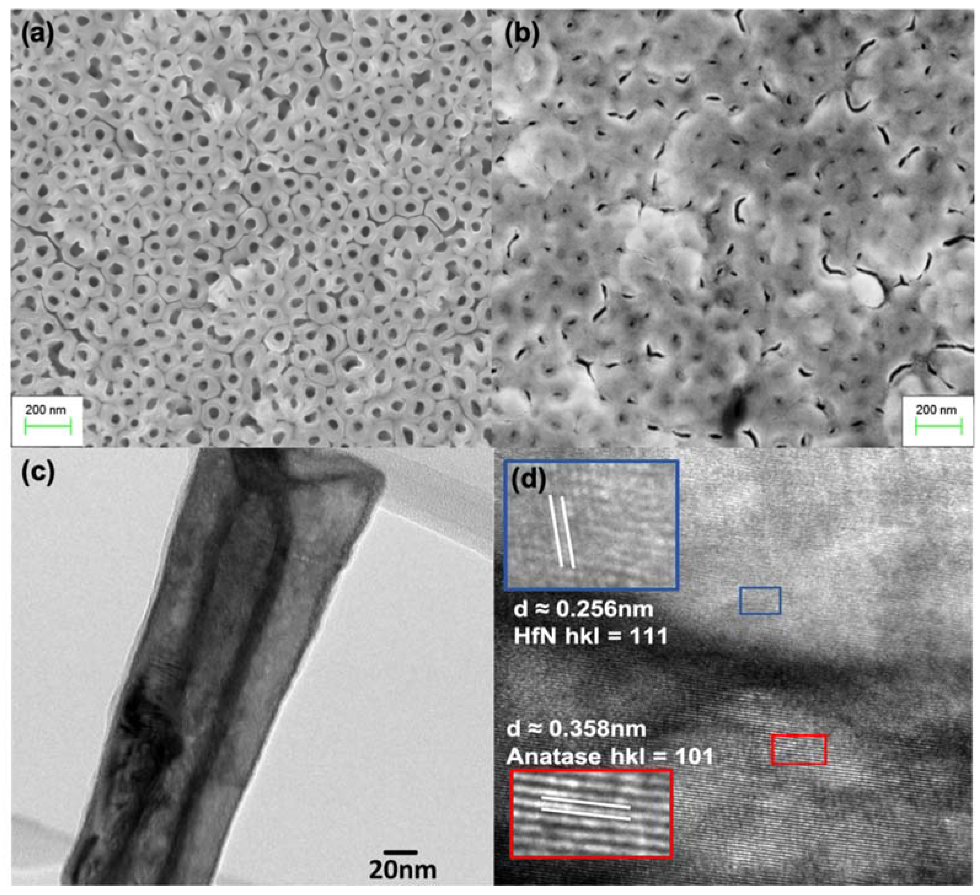
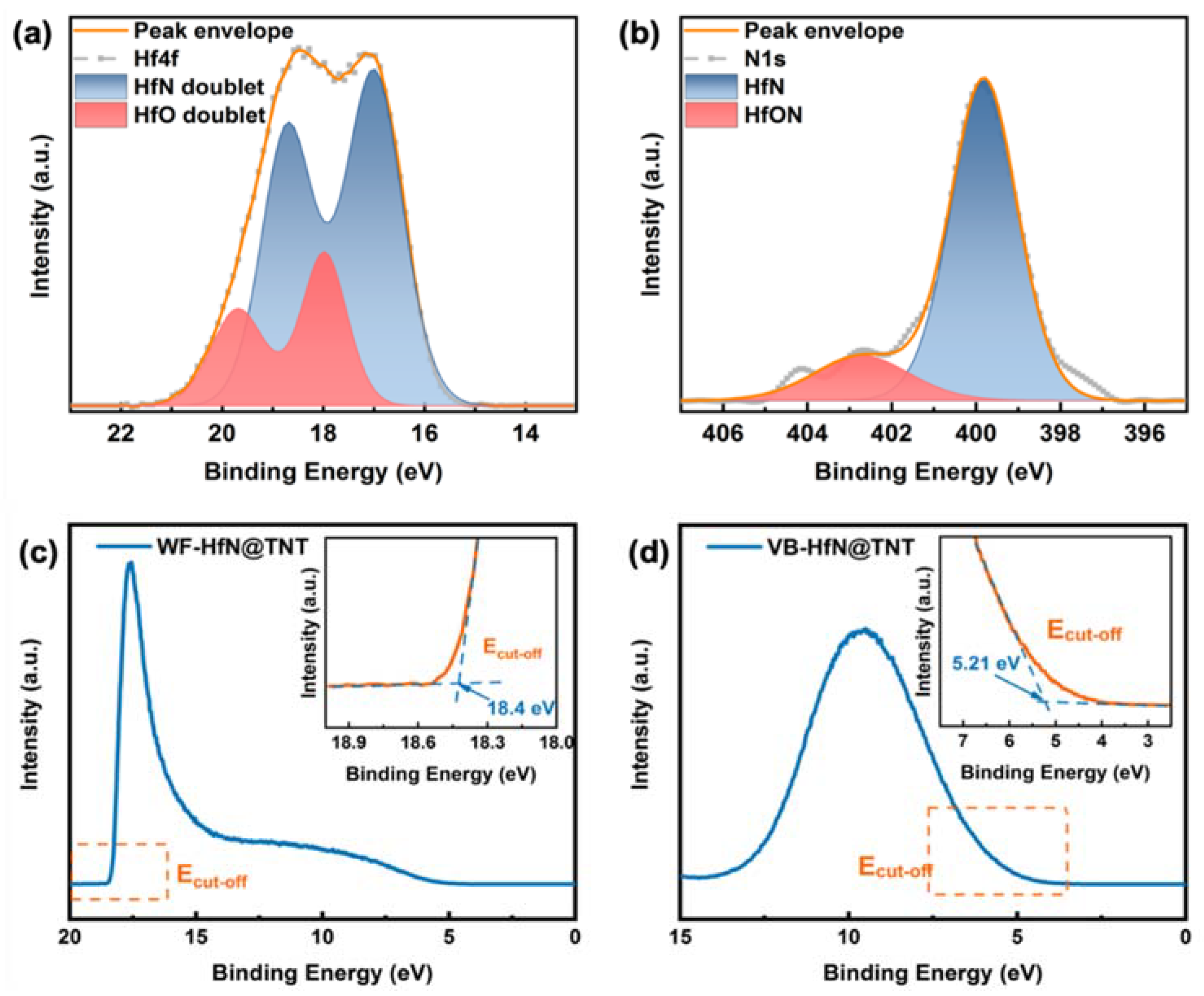
2.2. Physicochemical Characterization

The morphologies were examined before and after HfN coating using a Zeiss Sigma field emission scanning electron microscope (FESEM). The outer diameter of nanotubes is 80–100 nm, while the inner diameter is 30–50 nm (Figure 2a). After HfN atomic layer deposition (ALD), the mouths of nanotubes are almost closed, and the space between the nanotubes is filled. The high-resolution transmission microscopy (HRTEM) image (Figure 2c) shows the tubular structure with double layers. The TiO2 core is slightly brighter than the HfN shell, which is darker. Figure 2d shows the lattice fringes at the interface of the core and shell with 0.358 nm and 0.256 nm interplanar d-spacing, corresponding to anatase TiO2 (101) and HfN (111), respectively.
In the Hf 4f XPS spectrum (Figure 3a), the splitting of a spin orbit results in clear doublet peaks, which are Hf 4f5/2 and Hf 4f7/2. Thus, the peaks at 16.9 eV and 18.6 eV can be assigned to Hf 4f7/2-N and Hf 4f5/2-N bonds, respectively. Similarly, N1s (Figure 3b) also exhibited two major peaks at binding energies of 399.7 eV and 402.7 eV, which originated from HfN and HfON bonds, respectively [46]. The HfON is formed due to the surface oxidation in air environment. Since the HfN film was 20 nm thick and conformally coated throughout the sample, there is no trace of Ti 2p signal, which is too deep for detection by the high-resolution XPS measurement.
The value of work function was calculated using the equation: WF = 21.2 − Ecut-off in which Ecut-off is the energy of emitted secondary electrons and 21.2 eV is according to the He laser UV light source. The secondary electron cut-off energy of this material is 18.4 eV (Figure 3c). According to the expression given before, the work function with respect to the vacuum level is 2.8 eV, which is up shifted by 1.5 eV from the normal WF value of 4.3 eV for anatase TiO2 [24]. Additionally, the valence band maximum was calculated to be 5.21 eV (Figure 3d). Based on upward shifting and WF position, the material is electron degenerated after HfN coating due to its metallic property.
The phonon dispersion in HfN makes it an outstanding candidate for hot carrier-mediated photocatalysis. The constituent Hf and N atoms have a great difference in mass resulting in a large phonon gap between the optical and acoustic modes. In the Raman spectrum of the HfN-TNT sample (Figure 4a), the dominant four peaks are at 144 cm−1 (Eg), 399 cm−1 (B1g), 515 cm−1 (A1g and B1g), and 639 cm−1 (Eg) from anatase TiO2. Further investigation focused on HfN phonon dispersion. Although there are some peaks that do not stand out from TiO2 peaks, the signature Raman peaks for HfN phonon distribution are still noticeable. The peak representing the HfN transverse acoustic phonon mode is submerged in the TiO2 Eg band at 140 cm−1. Nevertheless, another signature peak for longitudinal acoustic phonons in the first-order acoustic band is observable at 199 cm−1 in the spectrum. The first-order optical phonon band is well resolved at 540 cm−1 and energetically distant from the first-order acoustic band. Other peaks, at 250 cm−1, 350 cm−1, 420 cm−1, 800 cm−1, and 1100 cm−1, can be assigned to second-order transverse acoustic mode, the sum of transverse and longitudinal acoustic modes, the difference between optical and acoustic modes, the sum of optical and acoustic modes, and second-order optical mode, respectively. It is worth noting that the first-order scattering peaks are not prominent in the Raman spectrum, which is due to the suppression of the first-order Raman effect by stoichiometric HfN with a low concentration of defects [47]. The source of first-order Raman scattering is usually attributed to N vacancies i.e., stoichiometric defects. The X-ray diffractogram (XRD) (Figure S1 in supporting information) indicates that HfN has a cubic fcc crystal structure, and the dominant (111) diffraction peak is a strong indication of stoichiometric HfN [48].
Klemens decay is the primary pathway for the loss of energy of optical phonons and is attenuated by a large phononic bandgap [49]. According to the Raman spectrum we presented in Figure 4a, the first-order acoustic and the first-order optical phonons were located at 140 cm−1 and 540 cm−1 respectively, meaning that the large energy difference between them prevents Klemens decay. This is a critical factor, because when the decay of optical phonons is suppressed, a phonon bottleneck is created and hot carriers tend to have a longer lifetime. HfN is a conductive ceramic with no electronic bandgap, which is a perfect characteristic for a hot carrier absorber [9]. The combination of these properties explains why we observed a small difference in photocurrent with and without a UV filter, obtaining a photocurrent response 1.74 mA·cm−2 and 2.39 mA·cm−2, respectively, at an applied bias of +0.6 V during on–off cycles. Incident photons stimulate plasmon oscillations on the sample surface, which then decay into hot electron–hole pairs through Landau damping. Due to the presence of applied bias and relatively longer hot carrier lifetimes in HfN, the high-energy holes were pushed to the anode–electrolyte interface prior to thermalization and oxidized the OH ions in the water-based electrolyte to form O2. From a thermodynamic point of view, holes with energies higher than 1.23 eV are capable of splitting water. According to the AM 1.5 G solar spectral irradiance data, the percentage of photon flux (vs the cumulative flux of photons in sunlight) up to 750 nm (practical cut-off wavelength) is 31% with UV filter and 36% without UV filter, which is in close agreement with the ratio of photocurrent we obtained with and without UV filter [50]. The conformal coating of HfN modified the optical properties of TiO2 nanotubes (Figure 4b). The band edge shifted from 385 nm (anatase TiO2) to 625 nm (HfN-TNT), thus enhancing visible light absorption. There also appeared a localized surface plasmon resonance (LSPR) peak centered at 720 nm with a Q factor equal to 0.95. Close to the LSPR peak, the maximum local electric field enhancement is observed at the HfN-TiO2 interface (Figure S3 in Supporting Information). The peaks after 800 nm are due to the interference fringes that are well-known for TiO2 nanotube arrays (Figure S4 in Supporting Information). It is worth noting that in the infrared regime, it displayed strongly increasing absorption, which indicated metal-like property due to high free carrier concentration.

2.3. Quantum Computation Results

The HOMO–LUMO plots (Figure 5) demonstrated that charge transfer excitation is prominent on HfN due to the fact that occupied and unoccupied regions are primarily composed of HfN orbitals, which is also supported by the projected density of states (PDOS) plot (Figure 6). Some tiny penetration of LUMO was observed in the close geometries, specifically in the case of TiO2 (101) and the Hf-terminated HfN (111) system. These results indicate that the HfN planes are chemically more active compared to TiO2. Figure 6a showed the PDOS of selected atoms in the HfN-TiO2 system, where TiO2 and HfN slabs are kept far apart to ensure there is no interaction between them. As expected, the plot showed TiO2 to be a wide bandgap n-type semiconductor whose valence and conduction bands are mostly composed of O-2p and Ti-3d states [51]. These figures also showed the electronic properties of HfN to be metallic with overlapped valence and conduction bands that are mostly composed of Hf d-states, which is consistent with earlier findings [8]. In the composite system, hot electron generation upon plasmon dephasing (Landau damping) within HfN is expected to be dominated by an intra-band transition involving the Hf d-orbital. These hot electrons can be injected into the TiO2 d-orbital from HfN in an indirect plasmon-induced charge transfer excitation route.
Note that according to the density of states analysis, the plasmon-induced chemical interface damping (CID) is not expected to play any significant role in the heterostructures. In the CID mechanism, plasmon dephasing occurs at the plasmonic metal–semiconductor interfacial region, where dephasing and the subsequent generation of hot electrons occur directly in the newly formed interfacial hybridized orbitals [52,53]. According to Figure 6b, almost no indication of the formation of such preferred hybridized orbitals in the vicinity of TiO2 conduction band edge is evident due to a large discrepancy in the DOS intensity and associated orbital types. The overlap between relevant HfN orbitals with TiO2 acceptor orbitals (in the conduction band region) was found to be inadequate for a CID-type mechanism to be dominant.

3. Materials and Methods

3.1. TiO2 Nanotube Array Synthesis

The fluorine-doped tin oxide (FTO)-coated glasses were first washed by soap water and then ultrasonicated in deionized water, acetone, and methanol sequentially for 10 min each. After being dried under a nitrogen stream, the top 3 mm of each substrate was covered with Kapton tape, which was done to keep an FTO-exposed area for contact in later experiments. Then, the substrates were loaded into a direct current magnetron sputtering system. The sputtering chamber was first evacuated to 10−6 Torr and later filled with argon to achieve a working pressure of 1 mTorr. A Ti target with 99.99% purity was used to deposit a 500 nm thick, smooth Ti film on the substrates at room temperature while benefiting from the atomic peening mechanism [54]. After deposition, the substrates were cut into 2.5 cm × 3 cm pieces with edges protected by Kapton tape to limited high currents at edges and corners during the electrochemical anodization process. The samples were anodized at 40 V in a mixed ethylene glycol-based electrolyte containing 0.3 wt% NH4F and 4 v% deionized water. The electrochemical anodization was conducted in a two-electrode cell using the as-prepared sample as the working electrode and a 6 mm diameter graphite rod as the counter electrode with a 3 cm distance between the anode and cathode. The anodization process took around 10 min until the current began to rise and the substrate turned semi-translucent from metallic dark. After the anodization completed, the samples were rinsed with methanol and dried under nitrogen flow. To remove the debris that formed on the top of the TiO2 nanotubes, a dry etching process was applied on synthesized samples using an Oxford PlasmaPro NGP80 Reactive Ion Etcher with SF6 as the working gas at 20 mTorr and a forward power of 250 W for 200 s, and it was followed by O2 plasma at 150 mTorr and a forward power of 225 W for 10 min. As-prepared samples were annealed in a three-zone tube furnace (STF55666C-1, Thermo Scientific Lindberg/Blue M), in which the temperature increased to 450 in 4 h and the dwell time was another 4 h.

3.2. ALD Deposition of Hafnium Nitride

HfN films were grown using a plasma-enhanced atomic layer deposition (PE-ALD) technique in a continuous flow ALD system (ALD150-LX, Kurt J. Lesker) at 1.01 Torr reactor pressure using remote inductively coupled plasma (13.56 MHz ICP, 0.6 kW, 60 sccm FG with 100 sccm Ar carrier). Tetrakis(dimethylamino)hafnium (TDMAHf) and forming gas (FG: 5% H2 + 95% N2) were the Hf-precursor and N-source, respectively. Process conditions for self-limiting HfN PEALD were characterized with in situ spectroscopic ellipsometry measurements (M2000DI, J. A. Woollam). Using growth-per-cycle (GPC) determined on a planar Si (111) substrate for PEALD cycle: 0.1 s TDMAHf pulse, 12 s post-precursor purge, 9 s FG plasma exposure, and 5 s post-plasma purge, 20 nm thick HfN film was grown on TiO2 nanotube array structures in 300 cycles.

3.3. Materials Characterization

The optical spectra of the TiO2@HfN nanotube arrays were measured in diffuse reflection mode using a UV-Vis-NIR spectrophotometer with an integrating sphere (Perkin Elmer Lambda 1050). The surface chemical composition was investigated by X-ray photoelectron spectroscopy (XPS) using a Kratos AXIS Ultra instrument, and the survey scan is shown as Figure S2 in the supporting information. To obtain the electronic structure information and band edge energy, the work function spectrum and valence band spectrum were acquired using ultraviolet photoelectron spectroscopy (UPS) using a He laser UV source.

3.4. Photoelectrochemical Measurements

The measurement of photoelectrochemical water splitting was performed in a three-electrode system consisting of the as-prepared sample photoanode, Pt cathode, and Ag/AgCl reference electrode, in KOH electrolyte. A Newport Oriel solar simulator with Class A output was used to generate simulated solar light (AM 1.5G), and the power density upon the sample surface was 100 mW/cm2. In order to measure the photocurrent response under visible light illumination, the simulated sun light (AM 1.5G) was filtered by a UV cut-off filter (λ > 420 nm). The photocurrent was obtained under linear sweep voltammetry mode, and the sweeping voltage was from −0.8 to +1.0 V versus Ag/AgCl. To investigate the photocurrent response of the sample at discrete wavelengths, near-monochromatic light LEDs were used to illuminate the sample at the power density of 10 mW/cm2. The photocurrent response was collected at a constant potential of 0.3 V vs. Ag/AgCl.

3.5. DFT Modeling

Structures of HfN-TNT composite systems for DFT calculations were built based on our collected X-ray diffractogram (XRD) data (shown in Figure S1 in the Supporting Information). The dominant TiO2 anatase plane (101) was used to build composite systems with HfN (111) and (200) planes. While HfN (200) planes have both Hf and N atoms, HfN (111) planes have either Hf or N terminated atoms. Thus, we have considered three planes of HfN with the (10) plane of anatase TiO2. All these three composite systems were constructed in both distant and proximate configurations. An OpenMx 3.9.2 (Open source package for Material eXplorer) package was used for density functional theory (DFT)-based quantum chemical calculations [55], where norm-conserving pseudopotentials [56] and pseudo-atomic localized basis functions [55] are implemented. The computational protocol involved two steps: geometry optimization followed by electronic property calculations using generalized gradient approximation (GGA) with Perdew–Burke–Ernzerhof (PBE) exchange-correlation functional [57]. Spin-polarization with periodic boundary conditions was employed for all the calculations. Hubbard U-corrections (DFT+U) were considered in our DFT model for considering the computational errors associated with on-site Coulomb interactions. The Hubbard U-value for Ti 3d orbitals was considered to be 3.3 eV [58]. This Hubbard U-correction provides an additional on-site Coulomb interaction to compensate for the inaccurate description of self-interaction particularly in a partially occupied TiO2 3d state [59]. In this approach, the additional functions force the electrons of a particular orbital (for TiO2 it is 3d orbital) to be more localized, thus ensuring the reproduction of experimental bandgaps [59]. The energy cut-off value was chosen to be 220 eV, while the threshold for convergence criterion for the self-consistent loop was set to be as small as 10−5. The Gaussian broadening method, with a broadening parameter of 0.08 eV, was used for the projected density of states (PDOS) plots. The highest occupied molecular orbital (HOMO) and lowest unoccupied molecular orbital (LUMO) were constructed using VMD (visual molecular dynamics) visualization software.

4. Conclusions

In this study, we reported a method for the fabrication of core–shell nanotube arrays consisting of a 20 nm ALD HfN shell and an anodic TiO2 nanotube support layer. To the best of our knowledge, it is the first report using HfN for photoelectrochemical water splitting. We observed excellent full visible regime photoactivity up to 730 nm for water splitting, and based on our literature survey, the photocurrent density is superior to any plasmonic noble metal-enhanced TiO2 based photoanodes. We consider the finding to be significant, as it demonstrated the far-reaching application potential of replacing active HER/HOR noble metals such as Au, Ag, Pt, Pd, etc. with lower-cost transition metal nitride ceramics. Moreover, the experimental results evidence two unique characteristics allowing a large population of long lifetime hot carriers, namely, a large bandgap between optical and acoustic phonon modes and the absence of an electronic bandgap, which particularly benefit hot carrier-based optoelectronic devices. It opens the window to a wide range of applications that enhance their performance using plasmonic noble metals including but not limited to photocatalysis, photosynthesis, dye degradation, and hot carrier solar cells.

Supplementary Materials

The following are available online at https://www.mdpi.com/article/10.3390/catal11111374/s1, Additional information on materials characterization and electromagnetic simulations, Figure S1: X-ray diffractogram of HfN-TNT sample illustrating material components by separating signals, Figure S2: XPS survey scan of HfN@TNT sample, Figure S3: Results of FDTD simulations of HfN-TNT showing electric field intensities for (a) xy plane and (b) xz plane at the resonant wavelength of 650 nm, Figure S4: Optical extinction spectrum of a bare TiO2 nanotube array, and Details related to the estimation of H2 generation yields.

Author Contributions

Conceptualization, S.Z., K.C.C. and K.S.; methodology, S.Z., T.M., E.V., P.K. K.M.M.A. and A.E.K.; validation, S.Z., T.M., S.R. and R.K.; formal analysis, S.Z., A.P.M. and P.K.; investigation, S.Z., T.M., S.R., K.M.M.A. and A.E.K.; resources, S.G. and K.S.; data curation, S.Z.; writing—original draft preparation, S.Z.; writing—review and editing, R.K., K.C.C. and K.S.; visualization, S.Z. and A.P.M.; supervision, S.G., K.S. and K.C.C.; project administration, S.G. and K.S.; funding acquisition, S.G. and K.S. All authors have read and agreed to the published version of the manuscript.

Funding

This research was funded by Future Energy Systems (FES) Canada First Research Excellence Fund, project T12-P02, Natural Sciences and Engineering Research Council of Canada (NSERC), grant number CREATE-463990-2015, and the National Research Council Canada (NRC)-University of Alberta NanoInitiative, project A1-014009. The APC was funded by Future Energy Systems.

Data Availability Statement

The data supporting the results and analyses presented in the paper are available upon reasonable request.

Acknowledgments

The authors utilized user-fee based characterization facilities at the University of Alberta nanoFAB. Kai Cui is acknowledged for collecting HRTEM data at the NRC Nanotechnology Research Centre. R.K. and A.P.M. thank NSERC for scholarship support. An Alberta Excellence Graduate Scholarship to S.Z. is acknowledged.

Conflicts of Interest

The authors declare no conflict of interest.

References

  1. Oyama, S.T. Introduction to the chemistry of transition metal carbides and nitrides. In The Chemistry of Transition Metal Carbides and Nitrides; Oyama, S.T., Ed.; Springer: Dordrecht, The Netherlands, 1996; pp. 1–27. [Google Scholar] [CrossRef]
  2. Guler, U.; Shalaev, V.M.; Boltasseva, A. Nanoparticle plasmonics: Going practical with transition metal nitrides. Mater. Today 2014, 18, 227–237. [Google Scholar] [CrossRef]
  3. Sproul, W.D. Hafnium nitride coatings prepared by very high rate reactive sputtering. Thin Solid Films 1984, 118, 279–284. [Google Scholar] [CrossRef]
  4. Karaballi, R.A.; Humagain, G.; Fleischman, B.R.A.; Dasog, M. Synthesis of Plasmonic Group-4 Nitride Nanocrystals by Solid-State Metathesis. Angew. Chem. Int. Ed. 2019, 58, 3147–3150. [Google Scholar] [CrossRef] [PubMed]
  5. Patsalas, P.; Kalfagiannis, N.; Kassavetis, S. Optical Properties and Plasmonic Performance of Titanium Nitride. Materials 2015, 8, 3128–3154. [Google Scholar] [CrossRef] [Green Version]
  6. Naik, G.V.; Schroeder, J.L.; Ni, X.; Kildishev, A.V.; Sands, T.D.; Boltasseva, A. Titanium nitride as a plasmonic material for visible and near-infrared wavelengths. Opt. Mater. Express 2012, 2, 478–489. [Google Scholar] [CrossRef] [Green Version]
  7. Farsinezhad, S.; Shanavas, T.; Mahdi, N.; Askar, A.M.; Kar, P.; Sharma, H.; Shankar, K. Core–shell titanium dioxide–titanium nitride nanotube arrays with near-infrared plasmon resonances. Nanotechnology 2018, 29, 154006. [Google Scholar] [CrossRef]
  8. Saha, B.; Acharya, J.; Sands, T.D.; Waghmare, U.V. Electronic structure, phonons, and thermal properties of ScN, ZrN, and HfN: A first-principles study. J. Appl. Phys. 2010, 107, 033715. [Google Scholar] [CrossRef] [Green Version]
  9. Chung, S.; Shrestha, S.; Wen, X.; Feng, Y.; Gupta, N.; Xia, H.; Yu, P.; Tang, J.; Conibeer, G. Hafnium nitride for hot carrier solar cells. Sol. Energy Mater. Sol. Cells 2016, 144, 781–786. [Google Scholar] [CrossRef]
  10. Defilippi, C.; Shinde, D.V.; Dang, Z.; Manna, L.; Hardacre, C.; Greer, A.J.; D’Agostino, C.; Giordano, C. HfN Nanoparticles: An Unexplored Catalyst for the Electrocatalytic Oxygen Evolution Reaction. Angew. Chem. Int. Ed. 2019, 58, 15464–15470. [Google Scholar] [CrossRef]
  11. Yang, X.; Zhao, F.; Yeh, Y.-W.; Selinsky, R.S.; Chen, Z.; Yao, N.; Tully, C.G.; Ju, Y.; Koel, B.E. Nitrogen-plasma treated hafnium oxyhydroxide as an efficient acid-stable electrocatalyst for hydrogen evolution and oxidation reactions. Nat. Commun. 2019, 10, 1–8. [Google Scholar] [CrossRef] [Green Version]
  12. Muneshwar, T.; Cadien, K. Comparing XPS on bare and capped ZrN films grown by plasma enhanced ALD: Effect of ambient oxidation. Appl. Surf. Sci. 2018, 435, 367–376. [Google Scholar] [CrossRef]
  13. Muneshwar, T.; Cadien, K. Low temperature plasma enhanced atomic layer deposition of conducting zirconium nitride films using tetrakis (dimethylamido) zirconium and forming gas (5% H2 + 95% N2) plasma. J. Vac. Sci. Technol. A 2015, 33, 31502. [Google Scholar] [CrossRef]
  14. Yang, Y.; Niu, S.; Han, D.; Liu, T.; Wang, G.; Li, Y. Progress in Developing Metal Oxide Nanomaterials for Photoelectrochemical Water Splitting. Adv. Energy Mater. 2017, 7, 1700555. [Google Scholar] [CrossRef]
  15. Kumar, P.; Thakur, U.K.; Alam, K.; Kar, P.; Kisslinger, R.; Zeng, S.; Patel, S.; Shankar, K. Arrays of TiO2 nanorods embedded with fluorine doped carbon nitride quantum dots (CNFQDs) for visible light driven water splitting. Carbon 2018, 137, 174–187. [Google Scholar] [CrossRef]
  16. Zeng, S.; Karthik, S.; Thakur, U.K.; Shankar, K. A review on photocatalytic CO2 reduction using perovskite oxide nanomaterials. Nanotechnology 2017, 29, 052001. [Google Scholar] [CrossRef]
  17. Kar, P.; Zeng, S.; Zhang, Y.; Vahidzadeh, E.; Manuel, A.; Kisslinger, R.; Alam, K.M.; Thakur, U.K.; Mahdi, N.; Kumar, P.; et al. High rate CO2 photoreduction using flame annealed TiO2 nanotubes. Appl. Catal. B Environ. 2018, 243, 522–536. [Google Scholar] [CrossRef]
  18. Kar, P.; Zhang, Y.; Farsinezhad, S.; Mohammadpour, A.; Wiltshire, B.D.; Sharma, H.; Shankar, K. Rutile phase n- and p-type anodic titania nanotube arrays with square-shaped pore morphologies. Chem. Commun. 2015, 51, 7816–7819. [Google Scholar] [CrossRef] [Green Version]
  19. Li, Z.; Zhang, L.; Liu, Y.; Shao, C.; Gao, Y.; Fan, F.; Wang, J.; Li, J.; Yan, J.; Li, R.; et al. Surface-Polarity-Induced Spatial Charge Separation Boosts Photocatalytic Overall Water Splitting on GaN Nanorod Arrays. Angew. Chem. Int. Ed. 2019, 59, 935–942. [Google Scholar] [CrossRef]
  20. Alam, K.M.; Jensen, C.E.; Kumar, P.; Hooper, R.W.; Bernard, G.M.; Patidar, A.; Manuel, A.P.; Amer, N.; Palmgren, A.; Purschke, D.N.; et al. Photocatalytic mechanism control and study of carrier dynamics in CdS@C3N5 core-shell nanowires. ACS Appl. Mater. Inter. 2021, 13, 47418–47439. [Google Scholar] [CrossRef]
  21. You, D.; Xu, C.; Wang, X.; Wang, J.; Su, W.; Wang, R.; Chen, T.; Wang, R.; Shi, Z. A core@dual-shell nanorod array with a cascading band configuration for enhanced photocatalytic properties and anti-photocorrosion. J. Mater. Chem. A 2020, 8, 3726–3734. [Google Scholar] [CrossRef]
  22. Heab, S.; Yanc, C.; Chena, X.Z.; Wanga, Z.; Ouyanga, T.; Guob, M.L.; Liua, Z.Q. Construction of core-shell heterojunction regulating α-Fe2O3 layer on CeO2 nanotube arrays enables highly efficient Z-scheme photoelectrocatalysis. Appl. Catal. B Environ. 2020, 276, 119138. [Google Scholar] [CrossRef]
  23. Jiang, H.; Chen, Y.; Li, L.; Liu, H.; Ren, C.; Liu, X.; Tian, G. Hierarchical ZnO nanorod/ZnFe2O4 nanosheet core/shell nanoarray decorated with PbS quantum dots for efficient photoelectrochemical water splitting. J. Alloy. Compd. 2020, 828, 154449. [Google Scholar] [CrossRef]
  24. Kumar, P.; Kar, P.; Manuel, A.P.; Zeng, S.; Thakur, U.K.; Alam, K.M.; Zhang, Y.; Kisslinger, R.; Cui, K.; Bernard, G.M.; et al. Noble Metal Free, Visible Light Driven Photocatalysis Using TiO2 Nanotube Arrays Sensitized by P-Doped C3N4 Quantum Dots. Adv. Opt. Mater. 2019, 8, 1901275. [Google Scholar] [CrossRef]
  25. Vahidzadeh, E.; Zeng, S.; Alam, K.M.; Kumar, P.; Riddell, S.; Chaulagain, N.; Gusarov, S.; Kobryn, A.E.; Shankar, K. Harvesting Hot Holes in Plasmon-Coupled Ultrathin Photoanodes for High-Performance Photoelectrochemical Water Splitting. ACS Appl. Mater. Interfaces 2021, 13, 42741–42752. [Google Scholar] [CrossRef]
  26. Manuel, A.; Shankar, K. Hot Electrons in TiO2–Noble Metal Nano-Heterojunctions: Fundamental Science and Applications in Photocatalysis. Nanomaterials 2021, 11, 1249. [Google Scholar] [CrossRef]
  27. Li, H.; Li, Z.; Yu, Y.; Ma, Y.; Yang, W.; Wang, F.; Yin, X.; Wang, X. Surface-Plasmon-Resonance-Enhanced Photoelectrochemical Water Splitting from Au-Nanoparticle-Decorated 3D TiO2 Nanorod Architectures. J. Phys. Chem. C 2017, 121, 12071–12079. [Google Scholar] [CrossRef]
  28. Zeng, S.; Vahidzadeh, E.; VanEssen, C.G.; Kar, P.; Kisslinger, R.; Goswami, A.; Zhang, Y.; Mahdi, N.; Riddell, S.; Kobryn, A.E.; et al. Optical control of selectivity of high rate CO2 photoreduction via interband- or hot electron Z-scheme reaction pathways in Au-TiO2 plasmonic photonic crystal photocatalyst. Appl. Catal. B Environ. 2020, 267, 118644. [Google Scholar] [CrossRef]
  29. Farsinezhad, S.; Sharma, H.; Shankar, K. Interfacial band alignment for photocatalytic charge separation in TiO2 nanotube arrays coated with CuPt nanoparticles. Phys. Chem. Chem. Phys. 2015, 17, 29723–29733. [Google Scholar] [CrossRef] [Green Version]
  30. Wei, R.-B.; Kuang, P.-Y.; Cheng, H.; Chen, Y.-B.; Long, J.-Y.; Zhang, M.-Y.; Liu, Z.-Q. Plasmon-Enhanced Photoelectrochemical Water Splitting on Gold Nanoparticle Decorated ZnO/CdS Nanotube Arrays. ACS Sustain. Chem. Eng. 2017, 5, 4249–4257. [Google Scholar] [CrossRef]
  31. Zheng, B.-F.; Ouyang, T.; Wang, Z.; Long, J.; Chen, Y.; Liu, Z.-Q. Enhanced plasmon-driven photoelectrocatalytic methanol oxidation on Au decorated α-Fe2O3 nanotube arrays. Chem. Commun. 2018, 54, 9583–9586. [Google Scholar] [CrossRef] [PubMed]
  32. Silva, G.S.T.; Carvalho, K.T.G.; Lopes, O.; Ribeiro, C. g-C3N4/Nb2O5 heterostructures tailored by sonochemical synthesis: Enhanced photocatalytic performance in oxidation of emerging pollutants driven by visible radiation. Appl. Catal. B Environ. 2017, 216, 70–79. [Google Scholar] [CrossRef]
  33. Ye, W.; Arif, M.; Fang, X.; Mushtaq, M.A.; Chen, X.; Yan, D. Efficient Photoelectrochemical Route for the Ambient Reduction of N2 to NH3 Based on Nanojunctions Assembled from MoS2 Nanosheets and TiO2. ACS Appl. Mater. Interfaces 2019, 11, 28809–28817. [Google Scholar] [CrossRef]
  34. Bhat, S.S.M.; Pawar, S.A.; Potphode, D.; Moon, C.-K.; Suh, J.M.; Kim, C.; Choi, S.; Patil, D.S.; Kim, J.-J.; Shin, J.C.; et al. Substantially enhanced photoelectrochemical performance of TiO2 nanorods/CdS nanocrystals heterojunction photoanode decorated with MoS2 nanosheets. Appl. Catal. B Environ. 2019, 259, 118102. [Google Scholar] [CrossRef]
  35. Sun, M.; Fang, Y.; Sun, S.; Wang, Y. Surface co-modification of TiO2 with N doping and Ag loading for enhanced visible-light photoactivity. RSC Adv. 2016, 6, 12272–12279. [Google Scholar] [CrossRef]
  36. Peng, C.; Wang, W.; Zhang, W.; Liang, Y.; Zhuo, L. Surface plasmon-driven photoelectrochemical water splitting of TiO2 nanowires decorated with Ag nanoparticles under visible light illumination. Appl. Surf. Sci. 2017, 420, 286–295. [Google Scholar] [CrossRef]
  37. Ge, M.-Z.; Cao, C.-Y.; Li, S.-H.; Tang, Y.-X.; Wang, L.-N.; Qi, N.; Huang, J.-Y.; Zhang, K.-Q.; Al-Deyab, S.S.; Lai, Y.-K. In situ plasmonic Ag nanoparticle anchored TiO2 nanotube arrays as visible-light-driven photocatalysts for enhanced water splitting. Nanoscale 2016, 8, 5226–5234. [Google Scholar] [CrossRef] [PubMed]
  38. Ingram, D.B.; Linic, S. Water Splitting on Composite Plasmonic-Metal/Semiconductor Photoelectrodes: Evidence for Selective Plasmon-Induced Formation of Charge Carriers near the Semiconductor Surface. J. Am. Chem. Soc. 2011, 133, 5202–5205. [Google Scholar] [CrossRef] [PubMed]
  39. Luo, J.; Li, D.; Yang, Y.; Liu, H.; Chen, J.; Wang, H. Preparation of Au/reduced graphene oxide/hydrogenated TiO2 nanotube arrays ternary composites for visible-light-driven photoelectrochemical water splitting. J. Alloy Compd. 2016, 661, 380–388. [Google Scholar] [CrossRef]
  40. Luo, J.; Chen, J.; Wang, H.; Liu, H. Ligand-exchange assisted preparation of plasmonic Au/TiO2 nanotube arrays photoanodes for visible-light-driven photoelectrochemical water splitting. J. Power Sources 2016, 303, 287–293. [Google Scholar] [CrossRef]
  41. Chen, J.; Bailey, C.S.; Hong, Y.; Wang, L.; Cai, Z.; Shen, L.; Hou, B.; Wang, Y.; Shi, H.; Sambur, J.; et al. Plasmon-Resonant Enhancement of Photocatalysis on Monolayer WSe2. ACS Photon. 2019, 6, 787–792. [Google Scholar] [CrossRef]
  42. Zhan, Z.; An, J.; Zhang, H.; Hansen, R.V.; Zheng, L. Three-Dimensional Plasmonic Photoanodes Based on Au-Embedded TiO2 Structures for Enhanced Visible-Light Water Splitting. ACS Appl. Mater. Interfaces 2014, 6, 1139–1144. [Google Scholar] [CrossRef] [PubMed]
  43. Su, F.; Wang, T.; Lv, R.; Zhang, J.; Zhang, P.; Lu, J.; Gong, J. Dendritic Au/TiO2 nanorod arrays for visible-light driven photoelectrochemical water splitting. Nanoscale 2013, 5, 9001–9009. [Google Scholar] [CrossRef]
  44. Pu, Y.-C.; Wang, G.; Chang, K.-D.; Ling, Y.; Lin, Y.-K.; Fitzmorris, B.C.; Liu, C.-M.; Lu, X.; Tong, Y.; Zhang, J.Z.; et al. Au Nanostructure-Decorated TiO2 Nanowires Exhibiting Photoactivity Across Entire UV-visible Region for Photoelectrochemical Water Splitting. Nano Lett. 2013, 13, 3817–3823. [Google Scholar] [CrossRef]
  45. Zhang, Z.; Zhang, L.; Hedhili, M.N.; Zhang, H.; Wang, P. Plasmonic Gold Nanocrystals Coupled with Photonic Crystal Seamlessly on TiO2 Nanotube Photoelectrodes for Efficient Visible Light Photoelectrochemical Water Splitting. Nano Lett. 2012, 13, 14–20. [Google Scholar] [CrossRef]
  46. Shinkai, S.; Sasaki, K. Influence of Sputtering Parameters on the Formation Process of High-Quality and Low-Resistivity HfN Thin Film. Jpn. J. Appl. Phys. 1999, 38, 2097–2102. [Google Scholar] [CrossRef]
  47. Stoehr, M.; Seo, H.-S.; Petrov, I.; Greene, J.E. Effect of off stoichiometry on Raman scattering from epitaxial and polycrystalline HfNx (0.85 ≤ x ≤ 1.50) grown on MgO(001). J. Appl. Phys. 2008, 104, 033507. [Google Scholar] [CrossRef]
  48. Yuan, L.; Fang, G.; Li, C.; Wang, M.; Liu, N.; Ai, L.; Cheng, Y.; Gao, H.; Zhao, X. Influence of N2 flow ratio on the properties of hafnium nitride thin films prepared by DC magnetron sputtering. Appl. Surf. Sci. 2007, 253, 8538–8542. [Google Scholar] [CrossRef]
  49. Chung, S.; Shrestha, S.; Wen, X.; Feng, Y.; Gupta, N.; Xia, H.; Yu, P.; Tang, J.; Conibeer, G. Evidence for a large phononic band gap leading to slow hot carrier thermalisation. IOP Conf. Series Mater. Sci. Eng. 2014, 68, 012002. [Google Scholar] [CrossRef] [Green Version]
  50. Kroon, R.; Lenes, M.; Hummelen, J.C.; Blom, P.W.M.; De Boer, B. Small Bandgap Polymers for Organic Solar Cells (Polymer Material Development in the Last 5 Years). Polym. Rev. 2008, 48, 531–582. [Google Scholar] [CrossRef]
  51. Moreno, J.J.G.; Nolan, M. Ab Initio Study of the Atomic Level Structure of the Rutile TiO2(110)–Titanium Nitride (TiN) Interface. ACS Appl. Mater. Interfaces 2017, 9, 38089–38100. [Google Scholar] [CrossRef] [PubMed]
  52. Ma, X.; Dai, Y.; Yu, L.; Huang, B.-B. Energy transfer in plasmonic photocatalytic composites. Light. Sci. Appl. 2016, 5, e16017. [Google Scholar] [CrossRef] [Green Version]
  53. Kale, M.J.; Avanesian, T.; Christopher, P. Direct Photocatalysis by Plasmonic Nanostructures. ACS Catal. 2013, 4, 116–128. [Google Scholar] [CrossRef]
  54. Farsinezhad, S.; Mohammadpour, A.; Dalrymple, A.N.; Geisinger, J.; Kar, P.; Brett, M.J.; Shankar, K. Transparent Anodic TiO2 Nanotube Arrays on Plastic Substrates for Disposable Biosensors and Flexible Electronics. J. Nanosci. Nanotechnol. 2013, 13, 2885–2891. [Google Scholar] [CrossRef]
  55. Ozaki, T. Variationally optimized atomic orbitals for large-scale electronic structures. Phys. Rev. B 2003, 67, 155108. [Google Scholar] [CrossRef]
  56. Bachelet, G.B.; Hamann, D.R.; Schlüter, M. Pseudopotentials that work: From H to Pu. Phys. Rev. B 1982, 26, 4199–4228. [Google Scholar] [CrossRef]
  57. Perdew, J.P.; Burke, K.; Ernzerhof, M. Generalized Gradient Approximation Made Simple. Phys. Rev. Lett. 1996, 77, 3865. [Google Scholar] [CrossRef] [Green Version]
  58. Dhifallah, M.; Iachella, M.; Dhouib, A.; Di Renzo, F.; Loffreda, D.; Guesmi, H. Support Effects Examined by a Comparative Theoretical Study of Au, Cu, and CuAu Nanoclusters on Rutile and Anatase Surfaces. J. Phys. Chem. C 2019, 123, 4892–4902. [Google Scholar] [CrossRef]
  59. Capdevila-Cortada, M.; Lodziana, Z.; López, N. Performance of DFT+U Approaches in the Study of Catalytic Materials. ACS Catal. 2016, 6, 8370–8379. [Google Scholar] [CrossRef] [Green Version]
Figure 1. Photocurrent density plots: (a) Photocurrent measured by linear sweep voltammetry under AM 1.5G illumination; (b) Photocurrent response during light on–off cycles, measured by linear sweep voltammetry under AM 1.5G illumination with and without UV cut-off filter (>420 nm); (c,d) Amperometric I-t curves showing photocurrent response under the illumination of near-monochromatic LEDs above at 0.3 V vs. Ag/AgCl.
Catalysts 11 01374 g001
Figure 2. FESEM images for sample before and after ALD HfN coating, (a,b) are top view images before and after HfN coating; (c) HRTEM cross-section view image demonstrates the two layers constituting the core–shell nanotube morphology; (d) HRTEM image at the HfN and TiO2 interface showing anatase TiO2 (101) lattice fringes and HfN (111) lattice fringes.
Catalysts 11 01374 g002
Figure 3. (a,b) Deconvoluted XPS spectra for Hf 4f and N 1s, respectively; (c,d) work function and valence band maximum with respect to vacuum level from ultraviolet photoelectron spectroscopy.
Catalysts 11 01374 g003
Figure 4. (a) Raman spectrum of HfN@TNT, TA stands for transverse acoustic mode, LA stands for longitudinal acoustic mode, O represents optical mode, and (b) UV-Vis absorption spectrum of HfN-TNT, and the inset is a zoom-in view of the localized surface plasmon resonance peak and its calculated quality factor.
Catalysts 11 01374 g004
Figure 5. DFT optimized structures showing spatial positions of highest occupied molecular orbital (HOMO) and lowest unoccupied molecular orbital (LUMO) for TiO2 (101) and HfN (111) are located at far (a) and close (b) configurations.
Catalysts 11 01374 g005
Figure 6. Projected density of states (PDOS) of selected atoms for HfN@TiO2 heterostructures in far and close configurations. TiO2 (101) and HfN (111) with Hf-edge planes are located at far (a) and close (b) configurations.
Catalysts 11 01374 g006
Table 1. A summary of photocurrent densities observed with plasmonic noble metal-decorated TiO2-based photoanodes for PEC water splitting under visible light illumination.
SamplePhotocurrent (µA/cm2)Light Intensity (mW/cm2)Light SpectrumApplied BiasElectrolyteReference
HfN-TNT1800100visible light (>420 nm)0.6 V1 M KOHThis work
Ag/N-TiO226120visible light (>420 nm)0 V0.5 M Na2SO4[35]
AgNPs/TiO2 NWs47100visible light (>420 nm)0.4 V0.1 M Na2SO4[36]
In situ AgNPs/TNTs4080visible light (>420 nm)0.3 V0.1 M Na2SO4[37]
Ag/N-TiO20.5500400–900 nm0.3 V1 M KOH[38]
Au/RGO/H-TNTs224100visible light (>400 nm)0.2 V1 M KOH[39]
LE-Au/TNTs202100visible light (>400 nm)0.2 V1 M KOH[40]
AuNPs/TiO2237000532 nm, 633 nm0 V1 M KOH[41]
Au embedded TiO23 visible light (>420 nm)0.2 V1 M KOH + 25% MeOH[42]
AuNPs/TiO2 BNRs125100visible light (>420 nm)0.5 V1 M KOH[43]
AuNPs/TiO2 NWs1173.3visible light (>430 nm)0 V1 M KOH[44]
AuNPs/TiO2 PhC150100visible light (>420 nm)0.2 V1 M KOH[45]
Publisher’s Note: MDPI stays neutral with regard to jurisdictional claims in published maps and institutional affiliations.

