Article

ASIR: Application-Specific Instruction-Set Router for NoC-Based MPSoCs

by
Jens Rettkowski
1,* and
Diana Göhringer
2
1
Embedded Systems of Information Technology (ESIT), Ruhr-Universität Bochum, 44801 Bochum, Germany
2
Adaptive Dynamic Systems, Technische Universität Dresden, 01069 Dresden, Germany
*
Author to whom correspondence should be addressed.
Computers 2018, 7(3), 38; https://doi.org/10.3390/computers7030038
Submission received: 30 April 2018 / Revised: 9 June 2018 / Accepted: 22 June 2018 / Published: 27 June 2018
(This article belongs to the Special Issue Multi-Core Systems-On-Chips Design and Optimization)

Abstract

:
The end of Dennard scaling led to the use of heterogeneous multi-processor systems-on-chip (MPSoCs). Heterogeneous MPSoCs provide a high efficiency in terms of energy and performance due to the fact that each processing element can be optimized for an application task. However, the evolution of MPSoCs shows a growing number of processing elements (PEs), which leads to tremendous communication costs, tending to become the performance bottleneck. Networks-on-chip (NoCs) are a promising and scalable intra-chip communication technology for MPSoCs. However, these technological advances require novel and effective programming methodologies to efficiently exploit them. This work presents a novel router architecture called application-specific instruction-set router (ASIR) for field-programmable-gate-arrays (FPGA)-based MPSoCs. It combines data transfers with application-specific processing by adding high-level synthesized processing units to routers of the NoC. The execution of application-specific operations during data exchange between PEs exploits efficiently the transmission time. Furthermore, the processing units can be programmed in C/C++ using high-level synthesis, and accordingly, they can be specifically optimized for an application. This approach enables transferred data to be processed by a processing element, such as a MicroBlaze processor, before the transmission or by a router during the transmission. Moreover, a static mapping algorithm for applications modeled by a Kahn process network-based graph is introduced that maps tasks to the MicroBlaze processors and processing units. The mapping algorithm optimizes the communication cost by allocating tasks to nearest neighboring PEs. This complete methodology significantly simplifies the design and programming of ASIR-based MPSoCs. Furthermore, it efficiently exploits the heterogeneity of processing capabilities inside the routers and MicroBlaze processors.

1. Introduction

The end of Dennard scaling led to the use of heterogeneous multi-processor systems-on-chip (MPSoCs) instead of scalar processors. The execution of an application on respective processing elements (PEs) that are optimized for specific tasks provide a high efficiency in terms of computation power related to energy [1]. However, the growing number of PEs increases the requirements regarding communication.
Therefore, particular care must be taken by selecting an appropriate communication infrastructure to fulfill the high requirements. Otherwise, the infrastructure tends to become the performance bottleneck of the overall system. Networks-on-chip (NoCs) are a promising communication infrastructure for MPSoCs containing a high number of PEs [1]. Communication methods from networks are applied and scaled-down to on-chip interconnect technology in NoCs. A NoC consists of several routers or switches that are connected via links to each other. A PE communicates with remaining PEs by transmitting data through routers until the message reaches its destination.
NoC-based MPSoCs can be integrated into field-programmable-gate-arrays (FPGAs) due to the sufficient amount of configurable logic cells. FPGAs provide high flexibility and computation power; however, the programming, as well as designing application-specific hardware, might be expensive and complicated, using hardware description languages such as VHDL and Verilog. High-level synthesis enables the programming of FPGAs using a programming language with higher abstraction [2]. Consequently, the productivity increases tremendously in designing hardware for FPGAs.
In addition to the rising design complexity, the programming complexity is tremendously increased by the heterogeneity and the rising number of PEs. Hence, parallel programming models and methodologies that try to increase the abstraction level simplify the software design and become a crucial role. Along with the programming of heterogeneous MPSoCs, the mapping of tasks from an application is essential and requires high expertise in the software, as well as the hardware, of the MPSoC. A lot of mapping algorithms exist to optimize different system properties, such as performance and energy. However, the novel approach presented in this article demands new mapping algorithms that efficiently exploit the hardware capabilities.
The work in this article introduces application-specific instruction-set routes (ASIRs) that are based on [3]. In [3], a router architecture consisting of a processing unit that can process transmitted data by an application-specific processing core is presented. The processing core can be designed with C/C++ using high-level synthesis, which provides high flexibility in terms of processing capability, as well as a higher abstraction of the design. The internal buffers of ASIRs are exchanged by such a processing unit, and consequently, incoming messages can be processed during the transmission. Thus, an ASIR-based MPSoC consists of processors, such as MicroBlaze (MB) processors [4], connected to a NoC, which executes application-specific operations using routers. Accordingly, the communication overhead is tremendously reduced. The work in [3] is extended by a programming methodology based on Kahn process networks (KPN) that simplifies the design of the software, as well as the hardware. A parallel application is modeled by a KPN-based graph containing nodes that represents processes for PEs or routers. These processes are statically mapped by a novel algorithm that optimizes the communication cost due to the allocation of processes to the nearest neighboring PEs. The architecture has been evaluated by an MPSoC implemented with MicroBlaze processors as PEs on a Xilinx Zynq FPGA. This MPSoC is compared to an MPSoC that uses a NoC without application-specific processing functionalities. The presented approach is 17.6% faster in executing an image processing algorithm that performs a grayscale conversion, a sobel filter, and a threshold operation. Furthermore, the communication time is exploited more efficiently by 42.8%.
This article is structured as follows. Section 2 presents related work. Section 3 explains the structure of ASIR and the design of processing cores using high-level synthesis. Afterwards, Section 4 describes the programming methodology, including the task mapping algorithm based on KPNs. The results in terms of area and performance are discussed in Section 5. Finally, a conclusion and future works are given in Section 6.

2. Related Work

2.1. Design of NoC-Based MPSoC

Application-specific MPSoCs can provide better energy efficiency and performance due to optimizations. An automated generation tool for custom MPSoC architectures called OOGen is described in [5]. Using OOGen, an application-specific MPSoC can be generated with intellectual property cores (IPs) for FPGAs, while these components are treated as classes that are modeled in an object-oriented language. In this work, another approach is used to reduce the complexity in the hardware design. In contrast to OOGen, routers are developed in Very High Speed Integrated Circuit Hardware Description Language (VHDL), and application-specific operations are implemented using high-level synthesis tools. OOGen may require an update of the IP components for new applications. The approach presented in this work synthesizes new applications with Vivado High-Level Synthesis.

2.2. High-Level Synthesis

Each router of the NoC can be equipped with an application-specific processing unit. This processing unit is implemented using Vivado High-Level Synthesis. The higher level of abstraction simplifies the programming of the FPGA system and shortens the time-to-market while addressing today’s high system complexity. A wide variety of applications that benefit from high-level synthesis (HLS) exists [6,7,8,9].
The authors of [6] present a Hardware/Software (HW/SW) co-design of an Orthogonal Frequency-Division Multiplexing (OFDM) receiver implemented on a Xilinx Zynq SoC. High-level synthesis is used to create fast IP cores for the high compute-intensive parts of the OFDM receiver. In [7], high-level synthesis is used to do a design space exploration of an error correction unit that performs low density parity checks. Such processing blocks are important for modern software-defined radio systems. Another use case for high-level synthesis is given in [8]. A model predictive control that requires an online solution of an optimization problem is developed by high-level synthesis tools. A strategy is proposed that exploits the arithmetic operations to solve such problems on a FPGA. The work presented in [9] offers a backend, using high-level synthesis for a domain-specific language called HIPACC. The main area of this domain-specific language is image processing for heterogeneous platforms. All these applications show the benefit of high-level synthesis and the importance of the current evolution of hardware design. Accordingly, [5,6,7,8,9] justify the usage of high-level synthesis in the presented approach.
In [10], an HLS-generated router was developed and compared to a buffered mesh router. The authors of [10] show that the HLS-generated router is 3.5× smaller and 2.5× faster in terms of the clock period. They also designed a router with Relative Location (RLOCS) attributes, consuming only 60 LUTs and 100 FFs. The focus of [10] is a highly lightweight NoC for FPGAs.
In this work, high-level synthesis is used to develop the internal processing units of a router. In this manner, the router design benefits, as do the abovementioned works, from the reduced development time, as well as the simplified programming, of FPGAs. Furthermore, the remaining components of the router are developed and optimized in VHDL as a base FPGA architecture, which provides compatible interfaces for high-level synthesized processing units. Using application-specific processing capabilities inside a router, the transmission time can be efficiently exploited.

2.3. Network-on-Chip

NoCs try to apply network methods to on-chip communication. In [11], the integration of FPGAs inside a network interface is discussed for efficient computations. In this paper, an on-chip solution is presented that integrates the processing capability into the router. This enables processing while the data is transmitted through the NoC. Processing capacity located at a network interface requires transmission out of the router to the network interface and back to the router, resulting in a greater delay, in contrast to the presented approach.
In most MPSoCs, the main focus is the optimization of the transmission time of the on-chip communication scheme. The work in [12] presents an overloaded code-division multiple access (CDMA) for on-chip communication. It optimizes performance by a crossbar using CDMA. The advantage of a CDMA block is fixed latency, reduced arbitration, and higher bandwidth compared to a general crossbar. Another approach providing predictable latency is XNoC [13], which is a time-division-multiplexed (TDM) circuit-switched NoC. It switches between different routes within a predictable latency. In addition, it adapts itself by reconfiguring PEs. The reconfiguration time is hidden by overlapping with communication.
The focus of the NoC developed in this paper is not a predictable latency. However, the presented approach can also be applied to TDM-based NoCs, which allows the prediction of transmission latencies provided that the application-specific processing unit is predictable.
In [14], the router microarchitecture has been optimized in terms of performance using three approaches. Two pipeline stages were added to the router by dividing the operations of the router into two. A modified backpressure flow control mechanism was implemented, which supports high frequency and pipelined operation, and different buffering schemes were explored to sustain low queuing delays.
All the previously mentioned approaches divide the execution time of an application into the processing time of the PEs and the communication time of the on-chip communication. The approach of this paper shifts parts of the processing time to the communication time. Data is not only processed on an application-specific basis by the PEs but also during data transfers. Accordingly, the communication time is used more efficiently than in other NoCs.
MPSoCs that use a shared memory system can benefit from in-memory computing. This approach also equips the memory with processing capabilities as PEs to use more efficiently the memory transfers. ReVamp [15] is a general-purpose computing platform based on resistive random access memory (RRAM) crossbar array. The resistive RAM crossbar array exploits the parallelism in computing multiple logic operations in the same word. ReVAMP is a Very Long Instruction Word (VLIW) architecture for in-memory computing. In [16], an in-memory reconfigurable architecture based on RRAM crossbar structure is presented. It achieves full programmability across computation and storage.
However, an MPSoC based on shared memory communications does not scale efficiently in terms of performance for an increasing number of PEs compared to a NoC. IPNoSys II [17] is a new programming model evaluated in a mesh-based NoC. The NoC is indirect and equipped with memory blocks instead of PEs for storing data and forwarding it through the NoC. The routers of IPNoSys II are able to execute general-purpose instructions during data transfers.
Compared to our work, MicroBlaze processors are attached to every router of a direct mesh-based NoC. This structure of MicroBlazes and routers capable of executing application-specific instructions provides more flexibility in terms of programming and functionalities.

2.4. Programming and Task Mapping

The programming and task mapping on such MPSoCs are complex and require novel approaches to handle this complexity. A survey of different mapping algorithms for static and dynamic workload is given in [18]. Kahn process networks (KPNs) are a model of computation and can be used for dataflow programming of distributed systems. It is a well-known and widely used model to program embedded systems.
Khasanov et al. [19] extended this model of computation to improve runtime adaptivity while providing implicit data parallelism on an ARM processor. This model is successfully used in a lot of systems due to its deterministic execution and good applicability for streaming applications. In [20], an execution model based on Kahn process networks is proposed for heterogeneous MPSoCs. The model contains a scalable scheduler that schedules the processes defined in the execution model on the MPSoCs. The heterogeneous MPSoC consists of general-purpose processing elements and specialized hardware modules that communicate via a shared memory. Contrary to [20], a static task mapping is developed based on KPNs for heterogeneous MPSoCs. The MPSoC implemented in this work uses a NoC to exchange data that provides higher scalability compared to a shared memory system. Moreover, the hardware architecture of the NoC uses efficiently the communication time and requires novel mapping algorithms. Task mapping on an MPSoC is presented in [21] using simulated annealing. In addition, an improved automatic parameter selection method for simulated annealing is explained. Applications mapped by this algorithm are modeled as KPNs. The simulated annealing algorithm is not appropriate for the heterogeneous MPSoC presented in this article, because the mapping of tasks inside a router and tasks on MicroBlaze processors have a strong dependence. This dependence complicates the finding process of a start solution or related solutions for mapping, and hence, new mapping algorithms are necessary.

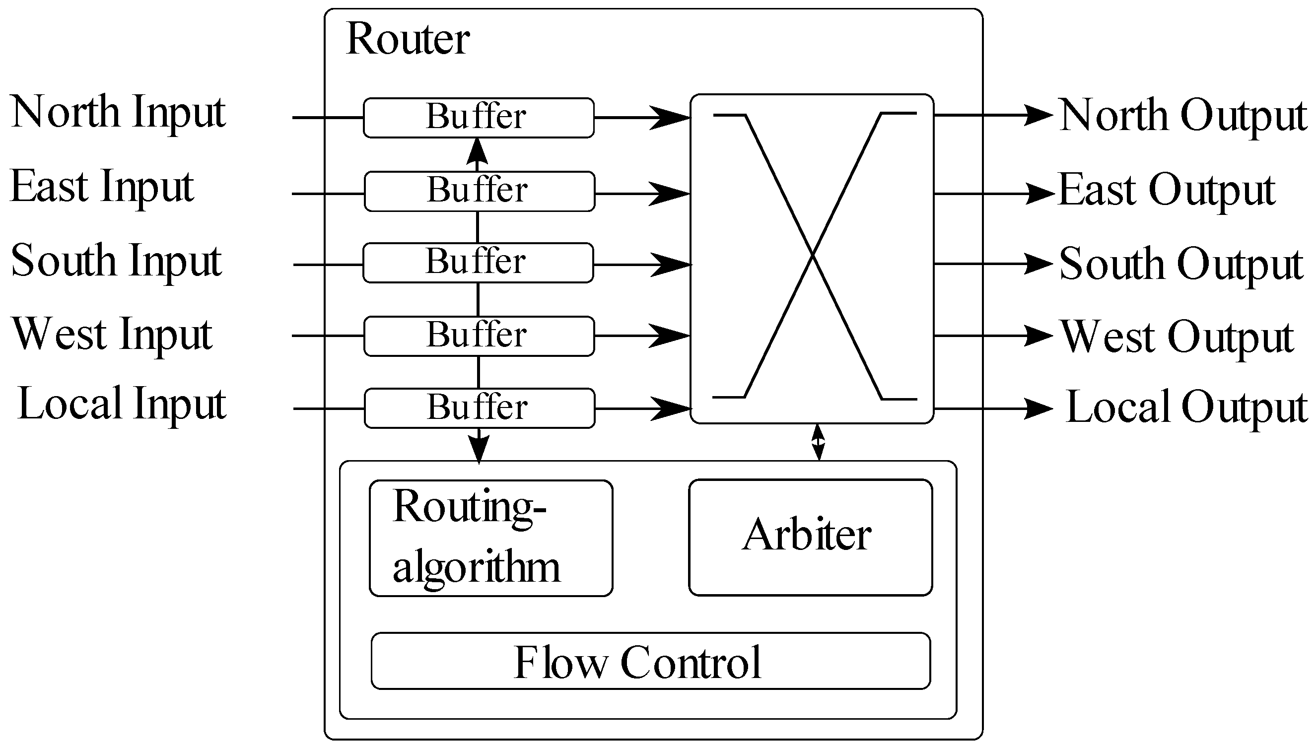
3. Hardware Architecture of ASIR

The novel router architecture ASIR is described in this Section. The routers are arranged in a two-dimensional (2D)-mesh topology, and they are addressable by a 3 bit X- and Y-coordinate. The 3 bit X- and Y-coordinate allows a maximum mesh size of 8 × 8. If a larger mesh topology is required, the bit width of the address can be adapted. However, the approach used in ASIR is not limited to a topology and therefore, can be also applied to other topologies, such as ring, torus, and spidergon. Figure 1 presents the internal structure of a generic router without application-specific functions. The routers have four input and output ports named after the directions (North, East, South, and West) and a local port that is directly connected to the corresponding PE. Routers located at the edges or corners have accordingly fewer ports. Every input port can be connected to any output port through a crossbar. The routing algorithm is locally computed inside the routers to determine the output port. An arbiter solves conflicts between multiple messages that try to access the same output port. In this work, the XY routing algorithm, a fixed priority arbiter, and wormhole routing [22] are used. The XY routing algorithm is a deterministic algorithm, which means that the path is only calculated by the source and destination address. Furthermore, the XY routing algorithm is minimal, and thus, it determines the shortest path between the source and destination address.
In contrast to round robin arbitration, a fixed priority arbiter uses fewer resources, but the presented approach works with round robin arbitration as well. A message consists of several flits, such as a header flit that contains the address of the destination, payload flits that contain the data, and a tail flit that determines the end of a message. Initially, a router analyzes the header flit to forward it to the respective output port while reserving the input buffer for every following flit corresponding to this message. The payload flits are forwarded to the same output port that has been passed by the header flit. The tail flit releases the reservation for other incoming messages. The buffer size is large enough to store a single flit. A handshake protocol between routers is implemented to store the data inside the buffers. In this way, data loss is avoided. The bit width of the ports is configurable and set to 32 bits.

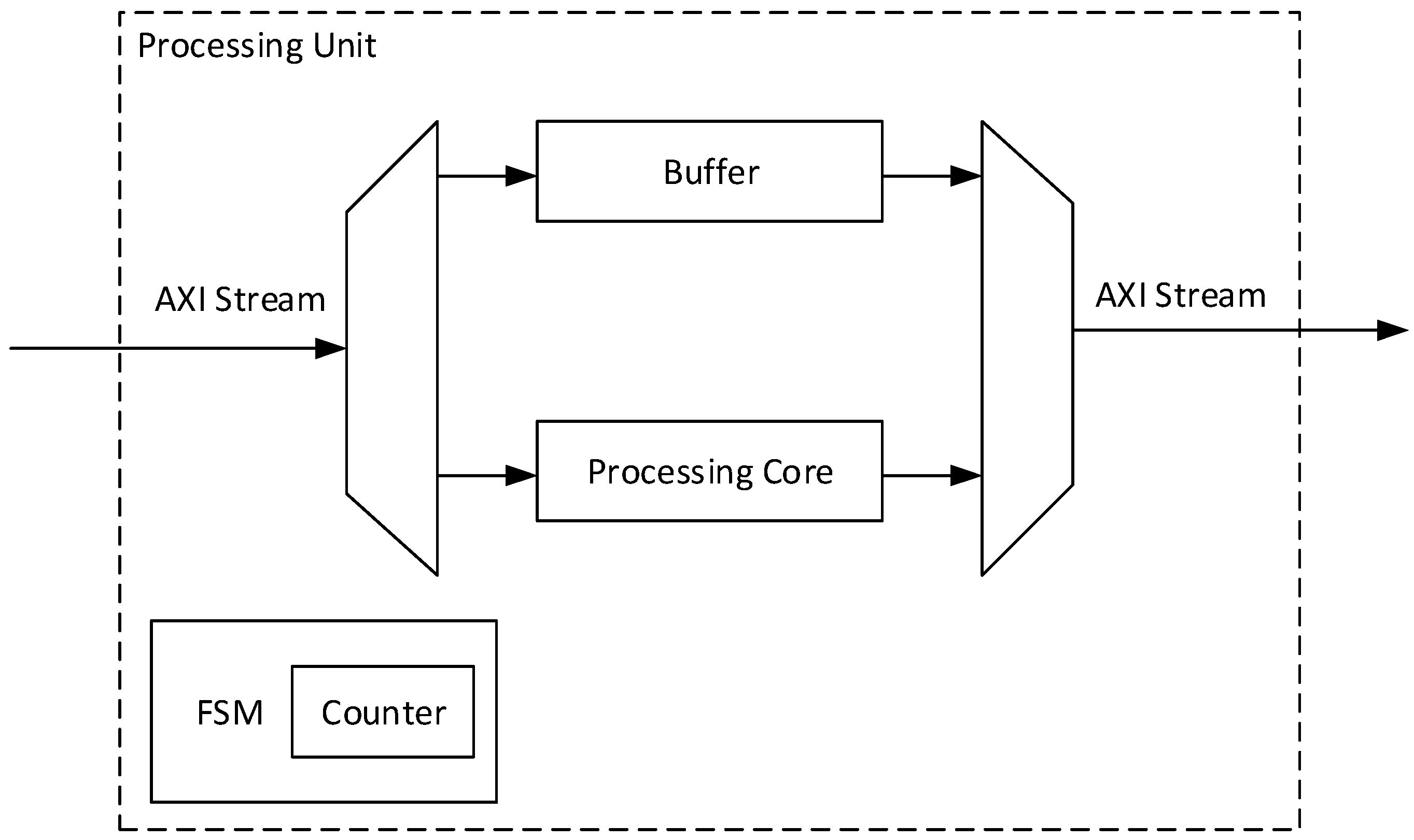
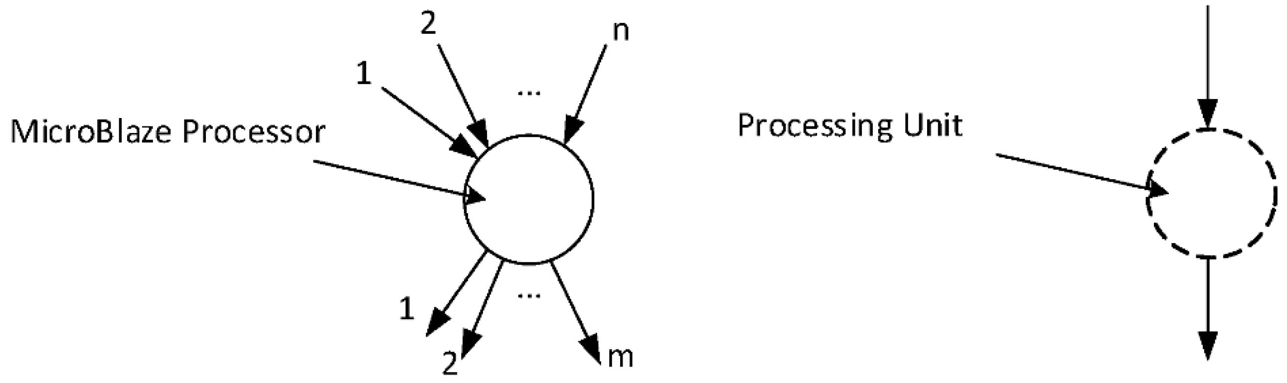
3.1. Processing Unit

Application-specific instructions are enabled by exchanging the input buffer with a processing unit, as shown in Figure 2. The number of input buffers that are exchanged by a processing unit depends on the application. By exchange of the internal buffer with a processing unit, transmitted flits can be directly processed during transmission. A processing unit attached to a network interface would require that the flits are forwarded out of the router to the processing core. Adding processing cores inside the routers enables the concatenation of processing cores by forwarding flits through multiple routers with processing cores. The concatenation of processing cores that are attached to a network interface requires higher effort in data transmissions, because processed flits must be forwarded to the network interface (NI) and back to the router. Accordingly, the presented approach provides better performance.
The processing unit consists of two multiplexers, a buffer, a processing core and a finite state machine (FSM) including a counter. Every core, except the processing core, is developed in VHDL without vendor-specific FPGA components. In this work, the processing core is synthesized with Vivado High-Level Synthesis 2017.2. The first multiplexer forwards incoming flits either to the buffer that stores the data without processing it or to the processing core, which performs the application-specific instruction. Because an Advanced Extensible Interface (AXI) stream is used as the communication protocol between routers, the buffer and the processing core also support AXI stream interfaces.
The second multiplexer transmits either the flits from the buffer or from the processing core out to the crossbar. An FSM controls the multiplexers, and therefore, it decides which flit will be processed by the processing core or forwarded through the buffer. Additionally, to the different types of flits in the wormhole routing, an instruction flit is defined. All flit types used in this work are shown in Figure 3. The header flit is composed of the destination address that determines the target router of the message, the source address that specifies the source router, a field containing the number of instruction flits, and a field containing tag information. The field representing the number of instruction is used by a network interface developed for MicroBlaze processors. An instruction flit is specified by an additional bit. It contains a 16-bit counter value and an instruction field, which determines at which router the data is processed. This counter value corresponds to the number of flits processed by the processing core. The bit width is configurable and is set to 16 for evaluation purposes. The FSM detects instruction flits, and based on the flits, it controls the processing core. If the specified instruction inside the flit corresponds to the router, it configures the multiplexers to forward messages through the processing unit until the counter from the FSM reaches the counter value specified in the instruction flit. The payload flits consist of 32 bits reserved for data, and the tail flit is specified by an additional bit.
As previously mentioned, the processing core is high-level synthesizable. Therefore, a template written in C has been developed for Vivado High-Level Synthesis 2017.2 that can be used to design processing cores. These cores can be directly integrated due to compatible interfaces. The template is used in Listing 1 to design a processing core providing a threshold function. The values of flits that are entering the processing core are compared to a threshold value of 110 in this threshold function. If it is lower than the threshold, the processing core sends a flit with a value of 0. If it is greater than the threshold, the processing core sends a flit with a value of 1. Other operations can be implemented using this template and are only limited by the high-level synthesis tool.
The input port of the processing core is represented by an integer pointer named A. The output port is represented by an integer pointer named B. Other data types can also be implemented. If the data type uses more than 32 bits, the bit width must be adapted to the data type. If it uses less than 32 bits, the bit width can be adapted until the minimum value of 22 bits. The minimum value is determined by the maximum number of necessary bits from the header flit or instruction flit.
Listing 1. C template that implements a threshold function in the processing core [3].
1:void processing_core(int* A, int* B){
2:#pragma HLS INTERFACE axis port=A
3:#pragma HLS INTERFACE axis port=B
4://Following code is application-specific
5:    int threshold=110;
6:    if (*A < threshold){
7:     *B=0;
8:    }else{
9:     *B=1;
10:    }
11:}
The router presented in this work is configured with an address size of 6 bits, a tag size of 6 bits, and a counter size of 16 bits. Accordingly, 18 bits (6 bits destination address + 6 bits source address + 6 bits tag) contain necessary information in the header flit. The instruction flit consists of 6 bits for the router address and 16 bits for the counter value, resulting in 22 bits. Therefore, the minimum bit width of a router which can be implemented is 22 bits in the presented configuration.
The pragmas written in lines 2 and 3 are necessary to provide compatible AXI stream interfaces. Furthermore, Vivado High-Level Synthesis generates control and status signals. These signals are necessary to reset and start the high-level synthesized core. The FSM ensures an error-free operation by setting these signals correctly. Using such processing cores, a router is able to process any function synthesized by Vivado High-Level Synthesis. A router for mesh topologies can contain up to five processing cores with different or the same operations. An efficient number of processing cores inside a router depends on the application and is determined at design time. Consequently, the development of a new application that exploits processing inside routers requires the selection and design of new processing cores.

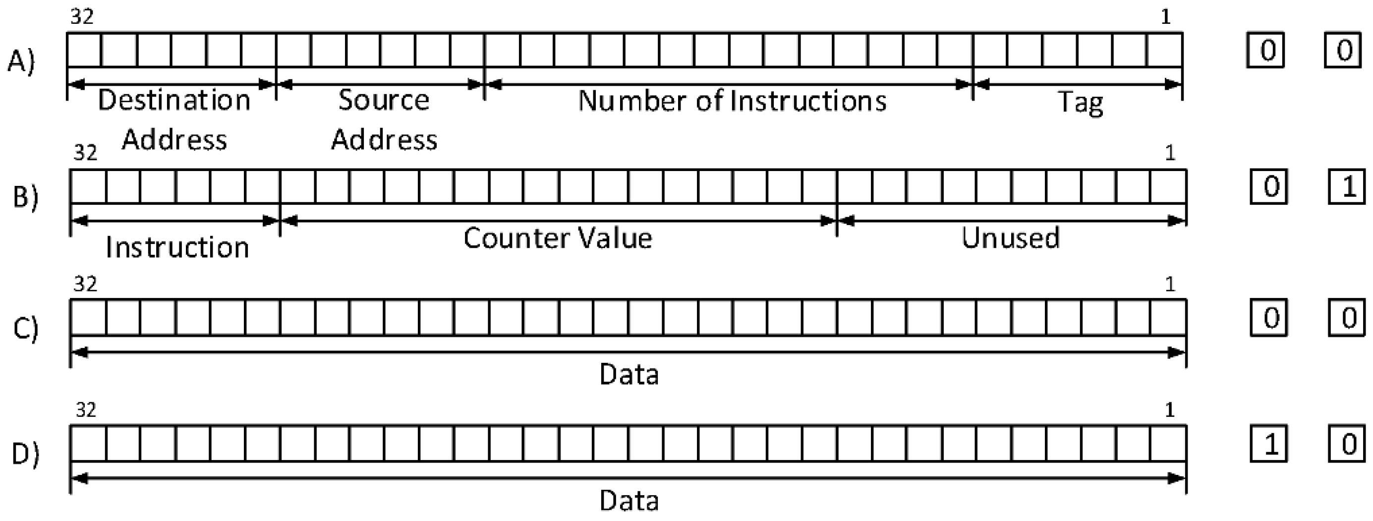
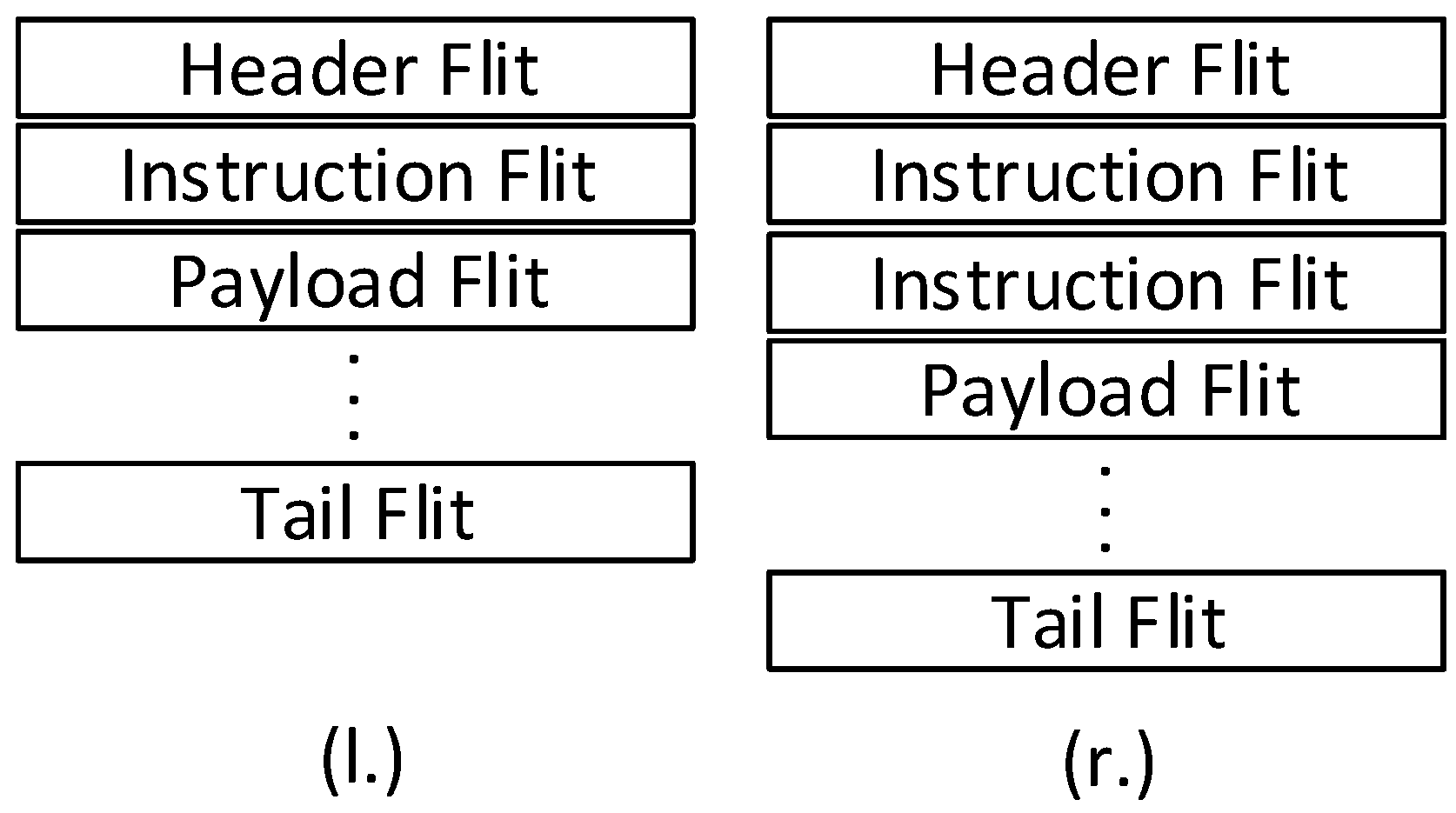
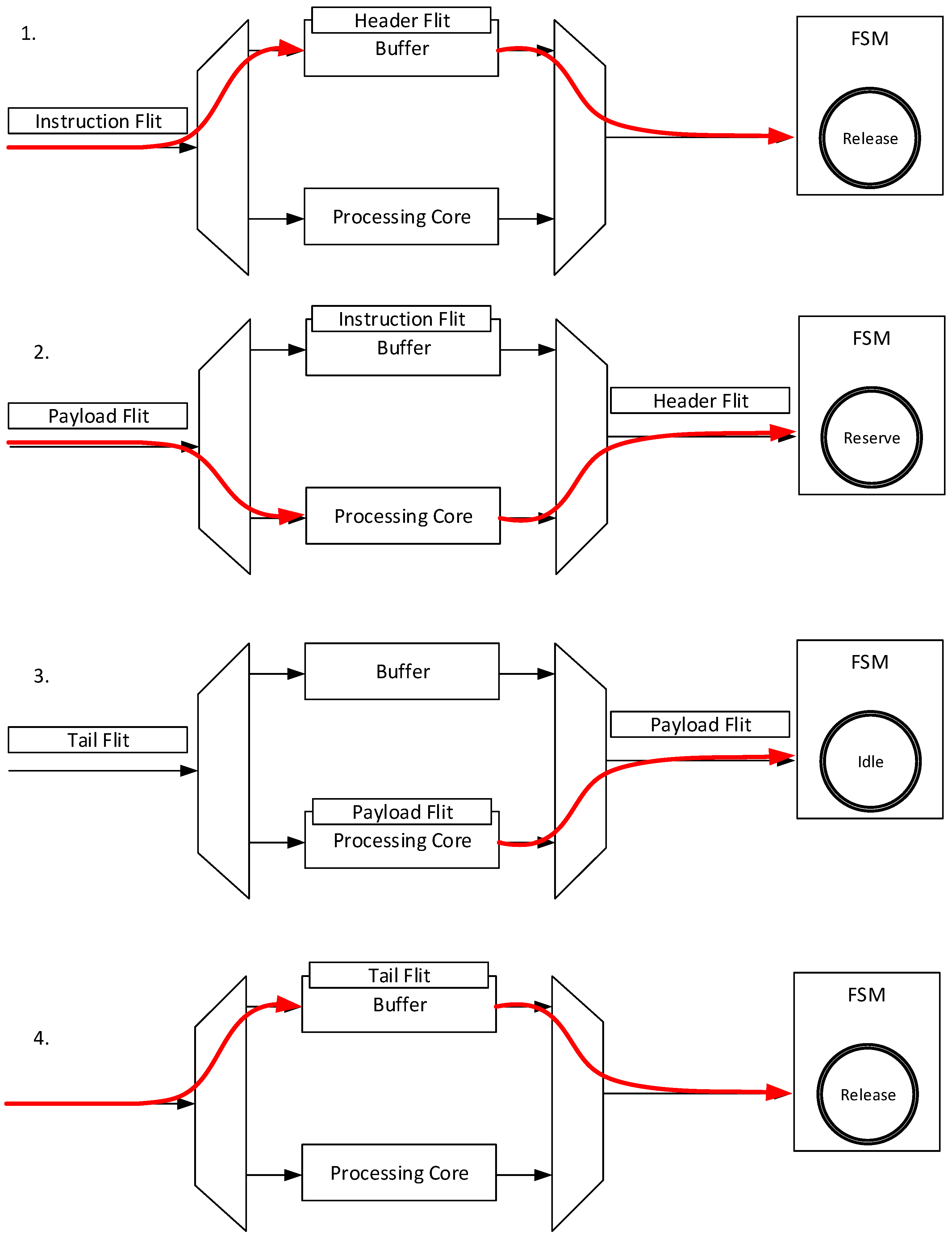
3.2. Instruction and Data Flow through the Processing Unit

A message contains four different types of flits: header flit, payload flit, instruction flit, and tail flit. If a message is transferred without an application-specific instruction, it contains only the header flit followed by payload flits and finally, the tail flit.
Figure 4 shows the construction of messages that are processed on an application-specific basis by a single router or two routers. The number of routers that processes a message is only limited by the topology and routing algorithm, because each flit has an additional bit to indicate if it is an instruction flit or not. MicroBlaze processors support a 32-bit AXI stream port. However, the total 32 bits are used for flits and cannot set the instruction bit. Hence, the interface analyzes the header flit regarding the number of instruction flits. The interface sets the instruction bit to ‘1′ for the number of flits that are defined in the header flit. Consequently, the instruction flits are sent directly after the header flit. The internal FSM of the processing unit has three states: Release, Reserve, and Idle state. Figure 5 describes the instruction and data flow of a message through the processing unit.
  • Initially, the FSM is in the Release state. The header flit of a message is forwarded through the first multiplexer to the buffer in this state. The second multiplexer transmits the output of the buffer to the crossbar. The configuration of the processing core by setting the control signals is also done in this state.
  • Afterwards, the instruction flit enters the buffer, which leads to a change from the Release state to the Reserve state. This state change requires that the instruction flit contains the corresponding address of the router; otherwise, the FSM remains in the Release state. The Reserve state sets the first and second multiplexer to the processing core. In addition, the counter increments at every incoming flit until it reaches the number of flits that is specified in the instruction flit. Furthermore, the instruction flit stored in the buffer is removed.
  • The FSM changes from the Reserve state to the Idle state at the moment when the counter reaches the specified number of flits. The Idle state disables the first multiplexer so that no new flit can be forwarded to the processing core, as well as the buffer.
  • The Release state is active again when the last flit of the processing unit has been transmitted. In Figure 5, the tail flit, which identifies the end of the message is transmitted through the buffer. However, further payload flits can be also transmitted.
In accordance with the presented approach, the flits that are processed by processing units are determined at compile time.

4. Programming and Mapping of ASIR-Based MPSoCs

ASIRs reduce efficiently the communication overhead in MPSoCs; however, the programming of the ASIR-based MPSoCs is complex without an appropriate methodology. This is due to the fact that the design space is tremendously increased by the heterogeneity of the ASIR-based MPSoCs. In addition to the mapping of processes on MicroBlaze processors, processing units must be mapped to routers as well. The mapping of MicroBlaze processes depends highly on the application, and thus, it must be conducted for each new application. Contrary to MicroBlaze processes, the mapping of processing units depends on the application and the routing algorithm that is supported by the NoC. In this work, a mapping based on a deterministic routing algorithm is implemented, which allows the precalculation of the whole path from source to destination. Therefore, a programming paradigm based on KPNs with a complete mapping algorithm is introduced.

4.1. Kahn Process Networks

A KPN is a widely accepted model of computation (MoC). KPNs are directed graphs, as shown in Figure 6, consisting of nodes that represent sequential processes and edges that correspond to communication channels between the processes. Communication channels are considered as unbounded First In—First Out buffers (FIFOs). A process that tries to read data out of an empty communication channel is suspended until the data arrives. That is why a read from a process is blocking. A process that writes through a communication channel is non-blocking, because the unbounded FIFOs are always able to receive data and forward it to the next process. A process can be modeled by two states: active and blocked. During the active state, a process can compute data or send data to another process. During the blocked state, a process waits for data while it tries to read it. Figure 6 describes an application modeled by a KPN that shows four processes: v1, v2, v3, and v4. v1 sends data to v2 and v3, while it is in the active state. Initially, v2 and v3 are in the blocked state and waiting for data from v1. After they received the data, v2 and v3 process the data and send it to v4, while the states are changed to active. V4 reads these data and process it.
In contrast to thread programming, KPNs cannot create race conditions, and it is obvious that this MoC is well-suited for streaming applications. All the properties mentioned previously allow KPNs to be efficiently executed by MPSoCs.

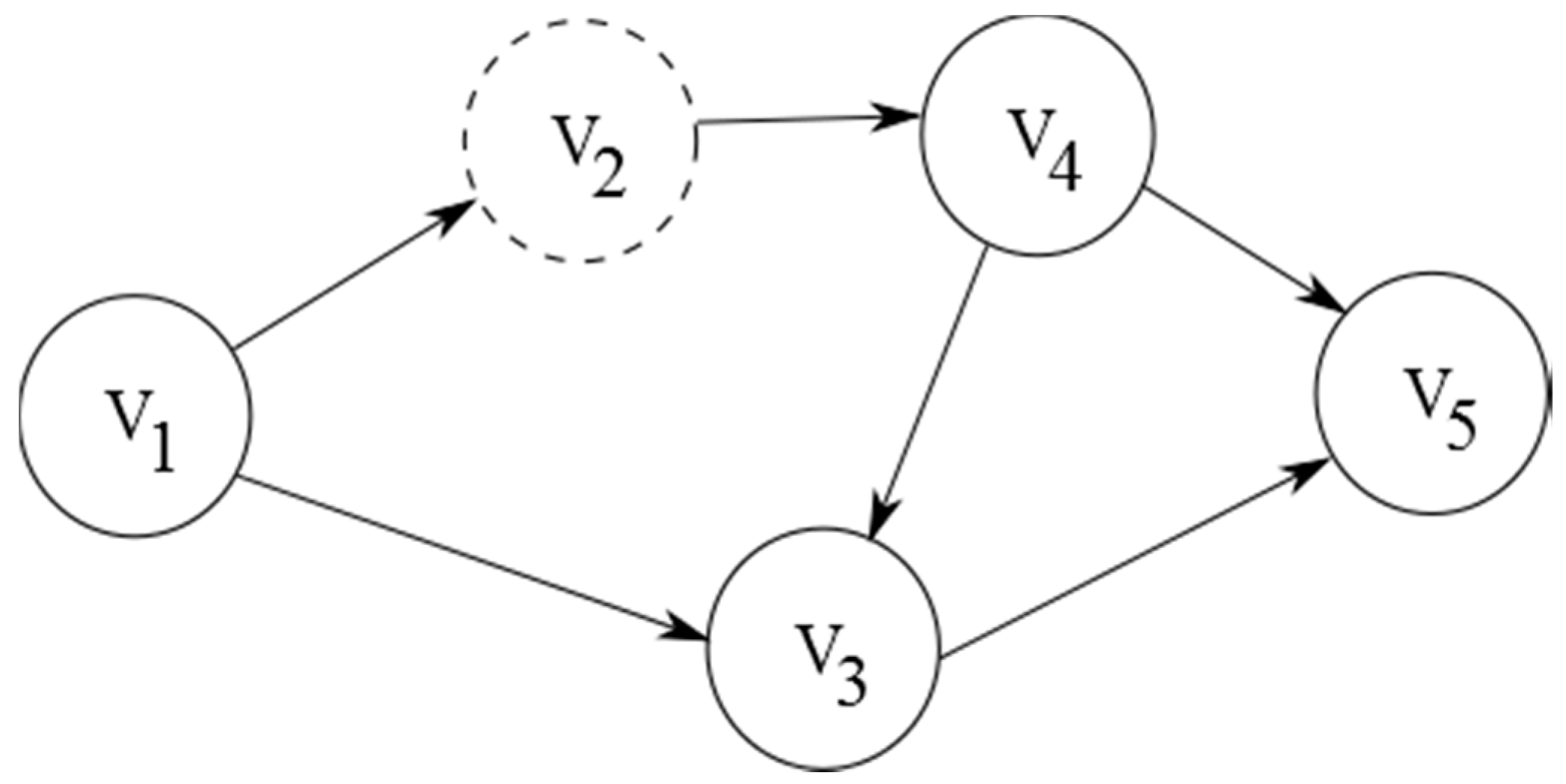
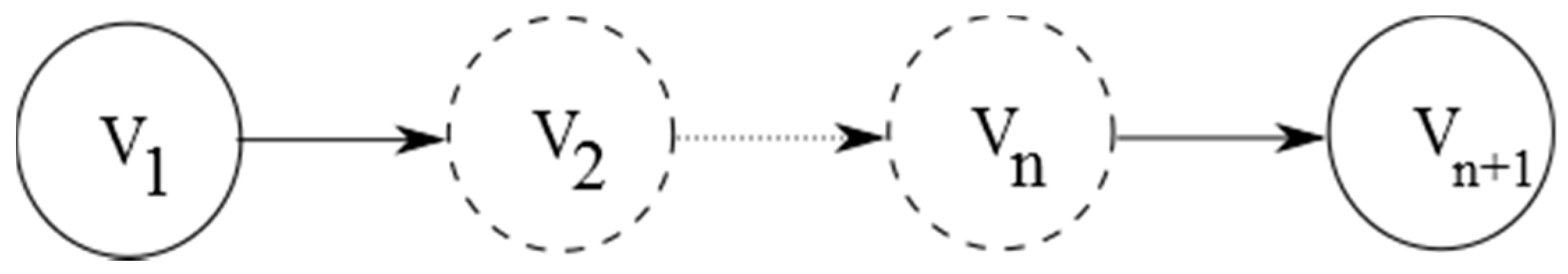
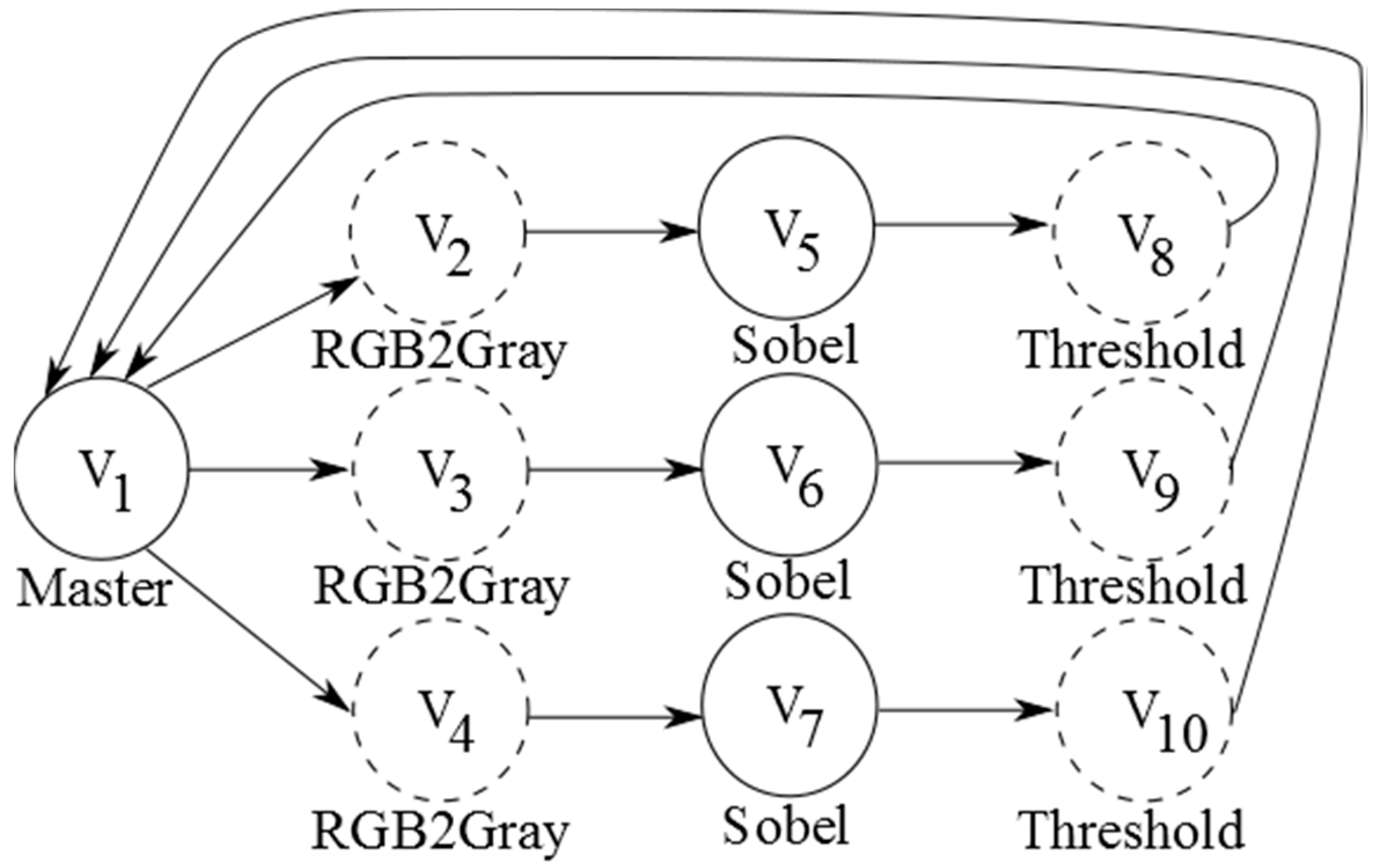
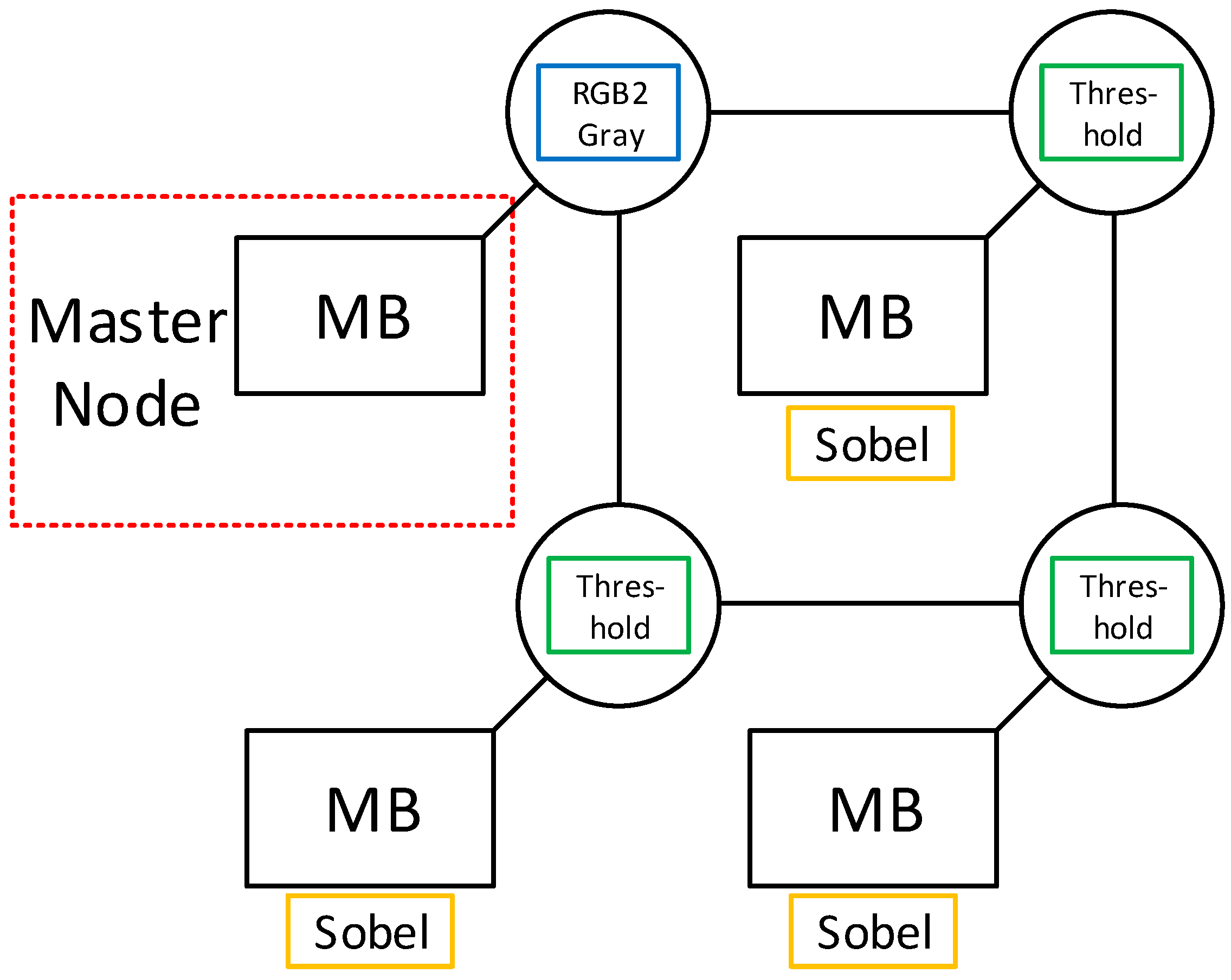
4.2. KPN-Based Graphs for ASIR-Based MPSoCs

The KPN is used as a programming model for ASIR-based MPSoCs that includes a mesh-based NoC and MicroBlaze processors as PEs. An application that should be executed on such an MPSoC can be modeled by a KPN. Each node of the KPN represents a process that can be executed by a MicroBlaze processor or a processing unit that is placed inside a router. In order to express this heterogeneity with a KPN, the model is extended by two different types of nodes, as shown in Figure 7. The type defines the type of PE that executes the process. The programmer that models the application has to decide if a process must be executed by a MicroBlaze processor or a processing unit. In future works, heuristics are planned that decide the type of PE for a node. Because a processing unit receives a message, executes an application-specific operation, and forwards the result to the next PE, a processing unit always has one incoming stream and one outgoing stream. Hence, a node for a processing unit must have one arc for the incoming stream and one arc for the outgoing stream.
In contrast to this, a node representing a process that is executed by a MicroBlaze processor can have any number of incoming and outgoing streams. Figure 8 shows an example of an application modeled by a KPN-based graph that shows the complete dataflow. The graph consists of five processes that are mapped on the MPSoC. Process v2, which has only one input and one output stream, is mapped to a processing unit of a router. The remaining processes are mapped to MicroBlaze processors. A graph can also contain a chain of multiple nodes that are mapped to routers. An example of a chain consisting of N + 1 processes is given by Figure 9. Nevertheless, this chain must receive data from a node (v1) and send data to a node (vN+1) that is mapped to MicroBlaze processors, because routers do not produce data, and they are not connected to IOs. Moreover, the first node that sends data to a router and the node at the end of the chain must be mapped to different MicroBlaze processors. Otherwise, the corresponding channel dependency graph for the mesh-based NoC creates a circle. This circle is a sufficient condition for a deadlock that can emerge.
Each node represents a process written in C/C++. A node that is mapped to a processing unit can be programmed using the template presented in Section 3.1. The MicroBlaze processors are programmed in C/C++ and use a lightweight software library, which is based on Message Passing Interface (MPI) to exchange data. This library provides an application programming interface (API), in which every node has a unique identification (ID) that is used to send and receive data between processes. This unique ID corresponds to the address inside the NoC and is defined by the mapping algorithm.

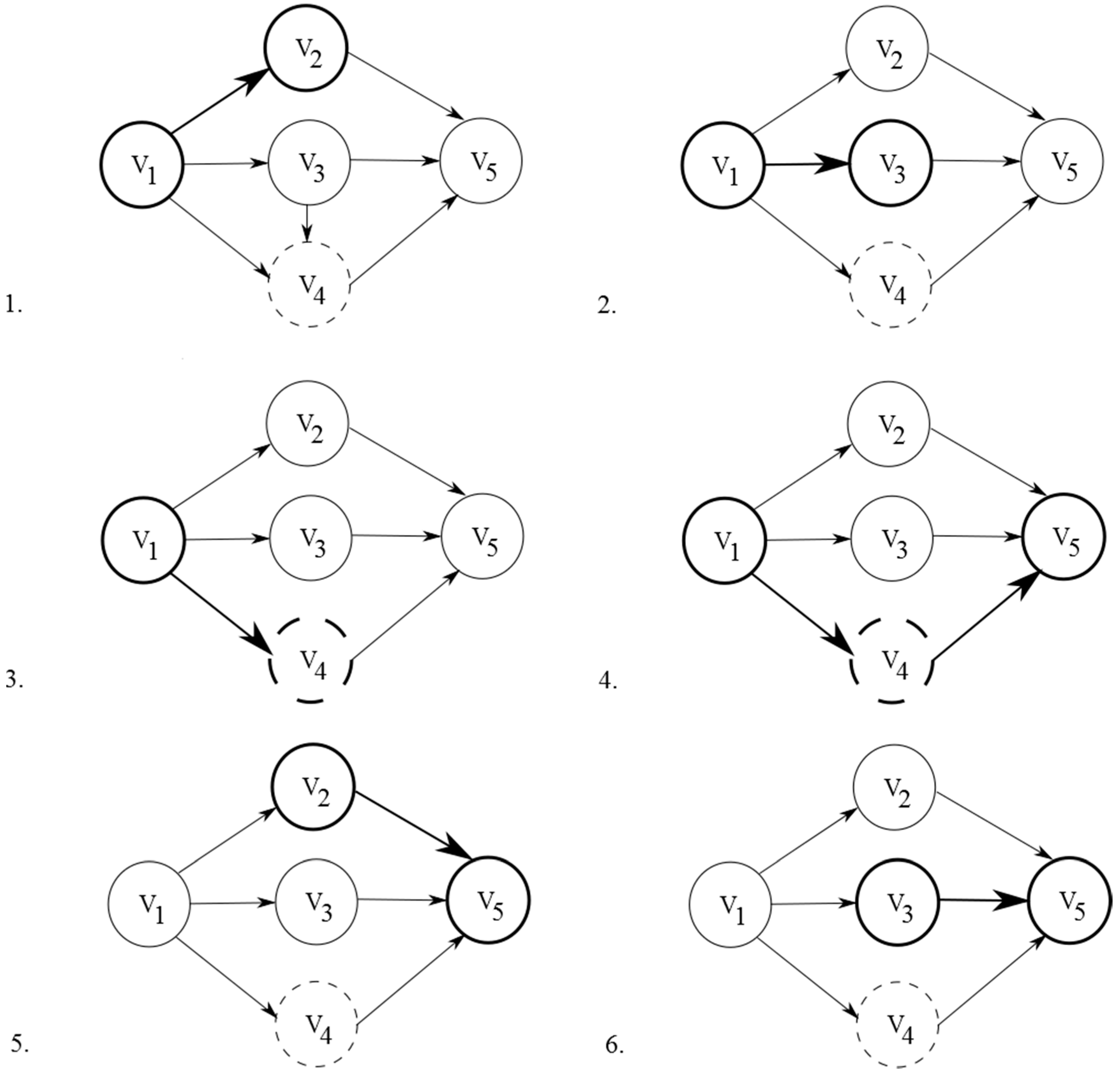
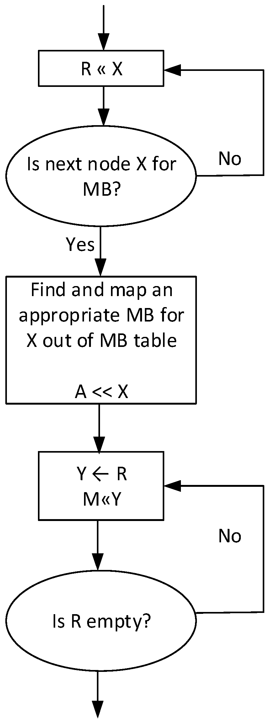
4.3. Mapping of KPN-Based Graphs on an ASIR-Based MPSoC

The mapping decides which routers are equipped with processing units. Therefore, the static mapping must be done before the bitstream is generated. Furthermore, the MicroBlaze processors exchange data with the lightweight software library. In this library, every MicroBlaze processor has a unique ID, which corresponds to an address inside the NoC. The address of each ID is determined by the mapping, and hence, it must be done before the MicroBlaze programs are compiled.
The static mapping algorithm analyzes the KPN-based graph until all nodes are mapped onto the MicroBlaze processors and routers. During the mapping, the communication cost between nodes is optimized by placing communicating nodes close to each other.
Figure 10 gives an overview of the steps executed by the mapping algorithm. An application modeled by a graph consisting of five nodes has to be mapped. Initially, the mapping algorithm allocates a MicroBlaze processor for the starting node v1. Afterwards, it maps all neighboring nodes from v1 to the MicroBlaze processors and routers, respectively (Step 1–3). The nodes are mapped to the closest available MicroBlaze processor, therefore optimizing the communication cost. Step 3 is a special case, because the mapping to routers depends on the application and on the routing algorithm, as aforementioned. Before a node is mapped to a router, the entire chain until the first node that is mapped to a MicroBlaze is determined. The algorithm begins with mapping the last node of the chain to an appropriate MicroBlaze processor (Step 4). Thus, the entire path from the source to the destination node can be calculated, and all nodes to routers can be mapped. After all nodes that are directly connected to v1 are mapped, it searches for all neighboring nodes from the next node v2 (Step 5). However, all neighboring nodes from v2 are already mapped, and therefore, it investigates the neighboring nodes from node v3 (Step 6). As node v3 is also only connected to mapped node v5, the mapping is complete, and the algorithm terminates.
A detailed program flow of the mapping algorithm is presented in Figure 11. In order to efficiently map the nodes, a mapping table is necessary that shows all available MicroBlaze processors and routers, as well as which node has been mapped to which PE. Table 1 shows an example of a 2 × 2 ASIR-based MPSoC after a complete mapping. Initially, the table is empty and contains only addresses of the available PEs, which are specified by the X and Y addresses of the NoC. Available PEs are the MicroBlaze processors and the input buffers (North (N), East (E), South (S), West (W), Local (L)) of all routers. During the mapping process, the available PEs are gradually updated with mapped nodes.
The KPN-based graph represented by G contains a set of vertices that represents N processes.
G = { v1, v2, …, vN}
Additionally, these nodes are connected by a set C representing m edges ei.
C = { e1, e2, …, em}
At the beginning of the algorithm, the starting node of graph G is mapped to a MicroBlaze processor (M << G) by adding it to the mapping table. The mapping table arranges all MicroBlaze processors with increasing path length. As the algorithm optimizes the communication cost, it always maps to the first free MicroBlaze processor, which has the shortest path length to the source node. The path length in terms of hops H between two addresses can be determined by Equation (3) for a mesh-based NoC.
H = |x1 − x2| + |y1 − y2| + 1,
A is a list, which is organized as a FIFO and contains nodes that are executed by MicroBlaze processors. Nodes that are added to this list are placed at the end of the list (A << G). Reading from this list provides and removes the first node. The list A ensures that all nodes are investigated before the algorithm terminates.
The active node S is the node from which all neighbors are analyzed. By reading the list A, the first element of it becomes the active node (S ← A).
The next step of the algorithm searches for the first neighboring node of active node S. This node is represented by X. A neighbor node can be found by searching for an edge that is connected to the active node S. In case node X will be mapped on a MicroBlaze processor, node X is added to the mapping table.
After the node X has been mapped, node X is added to the list A (A << X). Again, this ensures that after all neighbors of the active node S are analyzed, node X will also become the active node. When all neighbors of the active node S have been analyzed, the next node of list A becomes the active node. Afterwards, the algorithm checks again for adjacent nodes.
In the case that node X is mapped to a router, the algorithm determines the entire chain until a node must be mapped to a MicroBlaze processor again. A detailed flowchart of this part is given by Figure 12.
When all adjacent nodes of the active node S are mapped, the first element of list A is removed. If the list A is empty, the mapping is complete, and the algorithm terminates. If the list A is not empty, it sets the first element of list A to the next active node S.
Before the algorithm analyzes the neighbor nodes of the new active node S, the path lengths of the mapping table are updated. The source node for the new path length is the active node S. The following mapped nodes will have a minimum path length related to the active node S.
The mapping of nodes to routers is described in Figure 12, which is excluded from Figure 11, for the sake of clarity. In this part of the algorithm, another list R for routers is necessary, which is also structured as a FIFO. If list A would be used instead of R, the nodes inside the list must be distinguishable, because list R is only used to map processes that are executed by routers. Y represents the active node that should be mapped to a router. The first steps are to add all nodes to the list R, which should be mapped to routers until the first node for a MicroBlaze is found. The length of R defines the minimum path length inside the NoC to map all nodes to routers, because one node can be mapped to one router. This information is used to find a MicroBlaze processor for node X. The MicroBlaze processor must fulfill two requirements.
  • The path length to the MicroBlaze processor that executes the last mapped node must be greater than the length of R.
  • The routers that are used in this path must have enough available buffers free for all nodes in R.
Initially, the algorithm checks if the path length is long enough and afterwards, the number of available buffers inside this path. If one of the requirements is not fulfilled, it searches for another MicroBlaze processor with a path length that is equal to or greater than the previous path length. Every router has five buffers available for nodes; however, a message forwarded through the routers is not entering every buffer. Because the routing algorithm is the deterministic XY routing algorithm, the complete path can be calculated to any destination. A message that starts from address (x,y) enters first of all the local buffers (L) of the router located at the same address. If the next hop increases/decreases the X coordinate of the address, the message enters the east buffer (E)/west buffer (W) of the next router. If the next hop increases/decreases the Y coordinate of the address, the message enters the north buffer (N)/south buffer (S) of the next router. This methodology allows the algorithm to compute the number of available buffers for a given path.
After a possible path is found, the node at the end of the chain can be mapped to a MicroBlaze processor. Furthermore, this node is added to list A. As mentioned, list A contains all nodes for which the algorithm must still investigate their neighbor nodes. Therefore, this node must be added to list A after it is mapped (A << X).
All nodes of the chain that are executed by routers are listed in R and can be mapped using the mapping table, as well as the precalculated path. The first node of R can be always mapped to the local buffer inside the router at the same address in case it is free. In order to reduce the hardware overhead, the algorithm checks if the instructions that are executed by another chain of routers are the same. In case they are the same, the processing unit inside local buffer can be shared between these chains.
The presented algorithm cannot find a mapping solution when the number of processes exceeds the number of available PEs, because one node cannot be executed by multiple MicroBlaze processors or routers. Nevertheless, this algorithm is able to completely map an application described by a KPN-based graph on an MPSoC using ASIRs as long as enough PEs are available. However, it can be guaranteed that the algorithm terminates. The complexity of the algorithm increases along with the number of nodes and arcs in the KPN-based graph, as well as the network size. In order to decrease the complexity, a programmer can merge tasks to a single node, and accordingly, the number of nodes and arcs are reduced. In addition, the update of the mapping table can be changed to reduce the complexity.

5. Evaluation

ASIR is developed in VHDL and implemented on the xc7z020clg484-1 (ZedBoard) FPGA using Vivado 2017.2. The application-specific processing core is synthesized using Vivado High-Level Synthesis 2017.2. The system is evaluated by an image processing application, because image processing is used in various fields, such as medical imaging [23] and automotive applications [24].

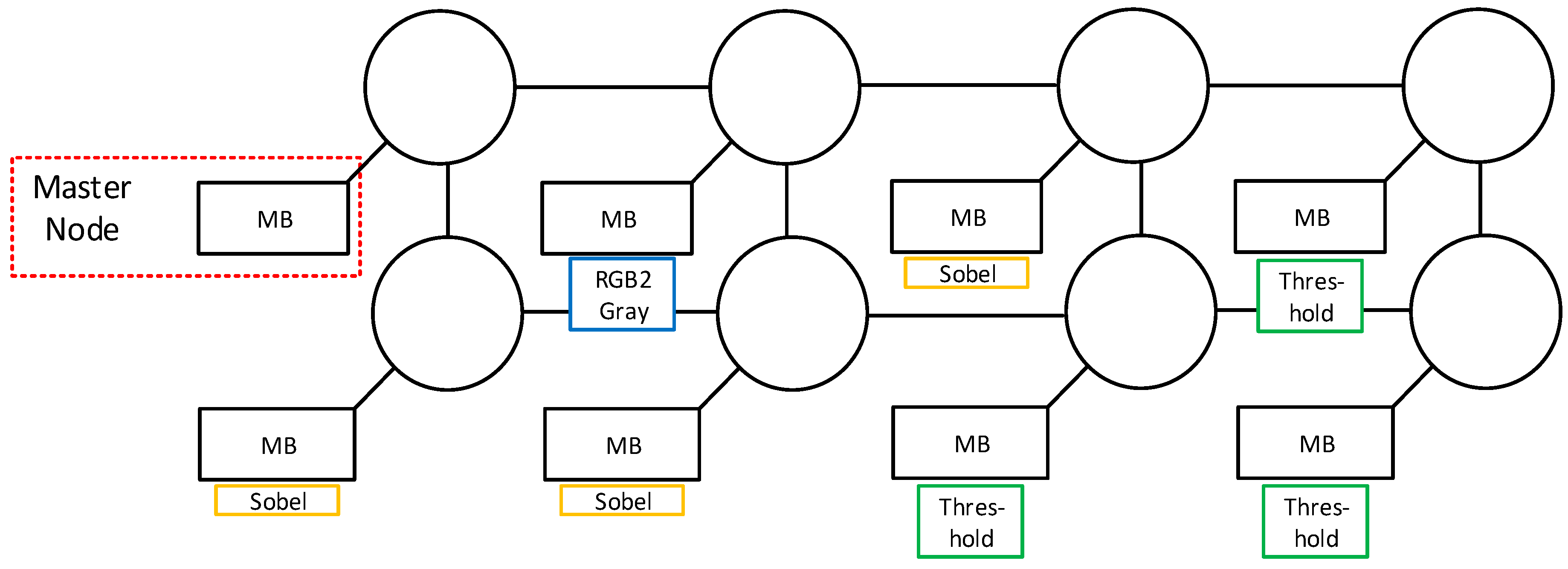
5.1. Image Processing Algorithm

Edge detection is a fundamental procedure in image segmentation, which is the process of dividing an image into multiple parts. Image segmentation is usually used to identify objects or other relevant information in images.
To evaluate ASIR and its programming methodology, an edge detection algorithm is implemented. The algorithm starts with a grayscale conversion of an image that is composed by 640 × 480 RGB pixels (red, green, blue). The corresponding grayscale value (gray) for a pixel is calculated by Equation (4).
gray = red + green + blue 3
Afterwards, the grayscale image is filtered by a sobel operator. The pixels values are compared to a threshold and respectively set to one or zero. The image resulting from these operations is a binary image, which reduces the amount of data that must be transferred.
Figure 13 shows this application modeled by a KPN-based graph for an ASIR-based MPSoC. The first node sends the data to the grayscale conversion followed by the sobel operator. Because the image is distributed to the MicroBlaze processors in order to benefit from the parallel processing, the first nodes send it three times to different nodes that process the same operation. This is due to the fact, that the grayscale conversion is mapped to routers, and these nodes are only allowed to have one input and one output stream, as mentioned. The sobel operation is performed by MicroBlaze processors, and the threshold operation is performed again by routers. This graph models the application in a manner that optimizes the data transmission. In all connections between different MicroBlaze processors, application-specific operations are executed that efficiently exploit the data transfer from one to another MicroBlaze processor. Figure 14 shows the corresponding mapping of the KPN-based graph. The circle in this graph is not creating a deadlock due to the fact that nodes (Sobel, Master) for different MicroBlaze processors are part of this circle. In contrast to the channel dependency graph, the application graph may contain circles as long as the circles consist of at least two nodes for the MicroBlaze processors. Otherwise, deadlocks can emerge. The processing unit performing the grayscale conversion (RGB2Gray) is mapped to the local port of the router. As a consequence, all messages that are sent from the master node to the remaining MicroBlaze processors are forwarded through ASIRs. Messages that are sent from any other MicroBlaze processor are forwarded through the processing unit with the threshold operation. Hence, the grayscale conversion is executed when the master node distributes the image. After the MicroBlaze processors have executed the sobel filter, the threshold operation is executed by the corresponding routers.
The graph from Figure 13 is mapped to a 2 × 2 mesh-based MPSoC with ASIRs and compared to two different MPSoCs using the previously mentioned image processing algorithm. The first MPSoC that is used for comparison is a 2 × 2 mesh-based MPSoC without ASIRs. The second MPSoC corresponds to a KPN-based graph, as shown in Figure 13, using only MicroBlaze processors to execute the processes. Accordingly, this MPSoC is a 2 × 4 mesh-based MPSoC providing the same number of parallel processing elements as the ASIR-based MPSoC. The ASIR-based MPSoC has four MicroBlaze processors and four processing units resulting in eight processing elements. The 2 × 4 mesh-based MPSoC is composed of eight processing elements. However, these processing elements only consist of MicroBlaze processors.
The image is equally distributed to three MicroBlaze processors in the 2 × 2 mesh-based MPSoC without ASIRs. These three MicroBlaze processors execute the grayscale conversion, the sobel filter, and the threshold operation in software. Afterwards, every MicroBlaze sends the respective part of processed image back to the master node. A timer is used by the master to measure the execution time of the image processing algorithm.
In the 2 × 4 mesh-based MPSoC, three MicroBlaze processors execute only the sobel filter, three MicroBlaze processors execute the threshold operation, and 1 MicroBlaze processor executes the RGB to gray conversion, as shown in Figure 15.

5.2. Resource Utilization

The resource utilization after synthesis of a single input buffer and the processing units (PU) with the threshold operation, as well as the grayscale conversion, is presented for an xc7z020clk484-1 Xilinx FPGA in Table 2. The resource utilizations of the different types of routers are presented in Table 3. The MicroBlaze processors are configured in the default configuration with 64 kB local memory. Table 4 presents the resource utilization of all the MPSoCs used in this work. The area overhead depends on how many processing units are inserted into the NoC. This decision must be made by the designer to fulfill the overall requirements of the application.

5.3. Performance Results

Figure 16 presents the execution times of the image processing algorithm. In addition, all MPSoCs are compared to a single MicroBlaze processor. It is important to mention that the comparison to a single MicroBlaze processor is not fair, because a single MicroBlaze processor cannot run multiple threads in parallel. The system that uses the single MicroBlaze processor is added to justify the absolute execution times of the MPSoCs. The frequency of the presented systems is 100 MHz.
A single MicroBlaze processor executes the application in 1.14 s. An ideal speedup of 3× can be assumed without consideration of communication costs for the 2 × 2 mesh-based MPSoC, because the image is distributed to three MicroBlaze processors. The results show that this MPSoC is 2.19× faster than the same algorithm implemented on a single MicroBlaze, which is reasonable due to the additional communication cost.
The MPSoC with ASIRs is 17.6% faster than the 2 × 2 mesh-based MPSoC without processing units and 59.1% faster than a single MicroBlaze.
The ideal speedup of 3× results in a best achievable execution time of 0.38 s. The MPSoC without processing units has a communication overhead of 0.14 s in contrast to the ideal execution time of 0.38 s. Accordingly, the MPSoC with processing units exploits the communication time 42.8% better, because it has only a communication overhead of 0.06 s.
The 2 × 4 mesh-based MPSoC without ASIRs requires 1.15 s, which is slower than a single MicroBlaze processor, although it provides the same number of parallel processing elements as the ASIR-based MPSoC. However, not all processing elements are used in parallel, as it can be seen in Figure 13. The RGB2Gray, sobel, and threshold operations are sequentially executed. Hence, the 2 × 4 mesh-based MPSoC cannot benefit from the eight processing elements. The communication overhead increases due to the integration of multiple MicroBlaze processors for each operation. This explains the performance breakdown compared to a single MicroBlaze processor. In contrast, the ASIR-based MPSoC uses the communication more efficiently, and that is why it provides the best speedup from the presented MPSoCs.

5.4. Discussion of Typical Use Cases

Typical use cases that can benefit from the presented approach consist of multiple processing stages. It is appropriate that the first processing stages perform pre-processing, such as sorting, conversion, and compression. These stages can be implemented in the routers and provide the pre-processed data to the MicroBlaze processors that perform the remaining processing stages. Benchmarks usually contain several applications, such as a matrix multiplication and a fast fourier transformation (FFT). These applications have only one processing stage to compute the final result. Hence, the system has been evaluated with a complete image processing application consisting of different processing stages. Furthermore, it is possible to use only routers as coprocessors that compute a complete streaming application. The KPN-graph represents the complete chain of processes; however, the node that sends data to the chain and receives data from the chain must be mapped to the different MicroBlaze processors, as mentioned. Therefore, nodes that represent processes mapped to the MicroBlaze processors can be placed in the beginning, at the end, and in the middle of the chain that splits it. The nodes that are mapped in the middle execute processes that only receive the data and forward it to the next router. The nodes that are mapped at the end of the chain execute processes that only receive the data and forward it back to the first node that started the chain. Accordingly, only routers perform the application-specific operations and execute a complete streaming application. Using this approach, the corresponding channel dependency graph does not contain any cycle, and hence, no deadlocks are created.
Generally, the ASIR-based MPSoC uses a direct NoC, and accordingly, every router is connected to a MicroBlaze processor. This resulted from the fact that the MPSoC will be able to execute multiple applications in parallel in future work, which requires sufficient computing resources. The general structure of a direct mesh-based NoC with enough processors is well-suited for the execution of multiple applications. However, it is also possible to remove a MicroBlaze processor that is not used in an application from the current MPSoC. The removal must be done manually during the hardware design, resulting in the reduction of hardware costs.

6. Conclusions and Outlook

This work presents ASIR, which is a novel router for NoC-based MPSoCs that executes application-specific instructions on messages during transmission, and a corresponding programming methodology. The innovation of ASIR is the exchange of the internal input buffer with a processing unit. The number of exchanges with processing units in a router depends on the application and is determined by a new task mapping algorithm. The internal structure of the processing unit consists of multiplexers, a high-level synthesized processing core, an internal buffer, and a finite state machine. The finite state machine controls the multiplexers to forward the message through the internal buffer or the processing core depending on incoming flits. Accordingly, a message is forwarded through the NoC that contains data and instructions. The processing core is generated using high-level synthesis, which in turn leads to a high flexibility because every part of a program can be synthesized in hardware limited only to the synthesis tool. To program such an ASIR-based MPSoC, the application can be modeled by a KPN-based graph, which is analyzed by a task mapping algorithm that allocates the task to the nearest neighboring PEs. Each node of the graph represents a C/C++-based process that is either compiled for a MicroBlaze processor or synthesized for a processing core. The mapping algorithm exploits efficiently the hardware capabilities, while simplifying the programming. An MPSoC using the presented routers is implemented and evaluated on a Xilinx Zynq FPGA by applying an image processing algorithm. Compared to an MPSoC that uses routers without application-specific processing, it executes an image processing algorithm 17.6% faster, while exploiting the communication time more efficiently by 42.8%.
In future works, dynamic partial reconfiguration will be applied to dynamically map the tasks on respective PEs.

Author Contributions

Conceptualization, J.R. and D.G.; Methodology, J.R. and D.G.; Software, J.R. and D.G. Validation, J.R. and D.G.; Original Manuscript Draft Preparation, J.R.; Manuscript Review and Editing, D.G.; and Supervision, D.G.

Funding

This research is funded by the German Research Foundation (DFG) via project SFB/TRR 196 “MARIE” through project S05.

Conflicts of Interest

The authors declare no conflict of interest.

References

  1. Gaur, M.S.; Laxmi, V.; Zwolinski, M.; Kumar, M.; Gupta, N. Network-on-chip: Current issues and challenges. In Proceedings of the 2015 19th International Symposium on VLSI Design and Test, Ahmedabad, India, 26–29 June 2015; pp. 1–3. [Google Scholar]
  2. Nane, R.; Sima, V.; Pilato, C.; Choi, J.; Fort, B.; Canis, A.; Chen, Y.T.; Hsiao, H.; Brown, S.; Ferrandi, F.; et al. A Survey and Evaluation of FPGA High-Level Synthesis Tools. IEEE Trans. Comput.-Aided Des. Integr. Circuits Syst. 2016, 35, 1591–1604. [Google Scholar] [CrossRef] [Green Version]
  3. Rettkowski, J.; Göhringer, D. Application-specific processing using high-level synthesis for networks-on-chip. In Proceedings of the 2017 International Conference on ReConFigurable Computing and FPGAs (ReConFig), Cancun, Mexico, 4–6 December 2017; pp. 1–7. [Google Scholar]
  4. Xilinx. MicroBlaze—Processor Reference Guide. UG984 (v2016.4). Available online: https://www.xilinx.com (accessed on 30 November 2016).
  5. Ding, H.; Ma, S.; Huang, M.; Andrews, D. OOGen: An Automated Generation Tool for Custom MPSoC Architectures Based on Object-Oriented Programming Methods. In Proceedings of the 2016 IEEE International Parallel and Distributed Processing Symposium Workshops (IPDPSW), Chicago, IL, USA, 23–27 May 2016; pp. 233–240. [Google Scholar]
  6. Sajjad, N.; Rettkowski, J.; Göhringer, D.; Nurmi, J. HW/SW Co-design of an IEEE 802.11a/g Receiver on Xilinx Zynq SoC using High-Level Synthesis. In Proceedings of the International Symposium on Highly-Efficient Accelerators and Reconfigurable Technologies (HEART), Bochum, Germany, 7–9 June 2017. [Google Scholar]
  7. Andrade, J.; George, N.; Karras, K.; Novo, D.; Pratas, F.; Sousa, L.; Ienne, P.; Falcao, G.; Silva, V. Design Space Exploration of LDPC Decoders using High-Level Synthesis. IEEE Access 2017, 5, 14600–14615. [Google Scholar] [CrossRef]
  8. Lucia, S.; Navarro, D.; Lucia, O.; Zometa, P.; Findeisen, R. Optimized FPGA Implementation of Model Predictive Control for Embedded Systems Using High Level Synthesis Tool. IEEE Trans. Ind. Inform. 2017, 14, 137–145. [Google Scholar] [CrossRef]
  9. Reiche, O.; Haublein, K.; Reichenbach, M.; Hannig, F.; Teich, J.; Fey, D. Automatic optimization of hardware accelerators for image processing. Workshop on Heterogeneous Architectures and Design Methods for Embedded Image Systems (HIS) in Proceedings of the DATE Friday. arXiv, 2015; 10–15arXiv:1502.07448. [Google Scholar]
  10. Kapre, N.; Gray, J. Hoplite: Building austere overlay NoCs for FPGAs. In Proceedings of the 2015 25th International Conference on Field Programmable Logic and Applications (FPL), London, UK, 2–4 September 2015; pp. 1–8. [Google Scholar]
  11. Underwood, K.D.; Sass, R.R.; Ligon, W.B. A reconfigurable extension to the network interface of beowulf clusters. In Proceedings of the 42nd IEEE Symposium on Foundations of Computer Science, Newport Beach, CA, USA, 8–11 October 2001; pp. 1552–5244. [Google Scholar]
  12. Ahmed, K.E.; Rizk, M.R.; Farag, M.M. Overloaded CDMA Crossbar for Network-On-Chip. IEEE Trans. Very Large Scale Integr. (VLSI) Syst. 2017, 25, 1842–1855. [Google Scholar] [CrossRef]
  13. Nguyen, T.D.A.; Kumar, A. XNoC: A non-intrusive TDM circuit-switched Network-on-Chip. In Proceedings of the 2016 26th International Conference on Field Programmable Logic and Applications (FPL), Lausanne, Switzerland, 29 August–2 September 2016; pp. 1–11. [Google Scholar]
  14. Chen, Q.; Liu, Q. Pipelined NoC router architecture design with buffer configuration exploration on FPGA. In Proceedings of the 2015 25th International Conference on Field Programmable Logic and Applications (FPL), London, UK, 2–4 September 2015. [Google Scholar]
  15. Bhattacharjee, D.; Devadoss, R.; Chattopadhyay, A. ReVAMP: ReRAM based VLIW architecture for in-memory computing. In Proceedings of the Design, Automation & Test in Europe Conference & Exhibition (DATE), Lausanne, Switzerland, 27–31 March 2017; pp. 782–787. [Google Scholar]
  16. Zha, Y.; Li, J. Reconfigurable in-memory computing with resistive memory crossbar. In Proceedings of the 2016 IEEE/ACM International Conference on Computer-Aided Design (ICCAD), Austin, TX, USA, 7–10 November 2016; pp. 1–8. [Google Scholar]
  17. Soares, R.B.S.; Silva, I.S.; Fernandes, S.R. IPNoSys II—A new architecture for IPNoSys programming model. In Proceedings of the 2015 28th Symposium on Integrated Circuits and Systems Design (SBCCI), Salvador, Brazil, 31 August–31 September 2015. [Google Scholar]
  18. Singh, A.K.; Shafique, M.; Kumar, A.; Henkel, J. Mapping on multi/many-core systems: Survey of current and emerging trends. In Proceedings of the 2013 50th ACM/EDAC/IEEE Design Automation Conference (DAC), Austin, TX, USA, 29 May–7 June 2013; pp. 1–10. [Google Scholar]
  19. Khansanov, R.; Goens, A.; Castrillon, J. Implicit Data-Parallelism in Kahn Process Networks: Bridging the MacQueen Gap. In Proceedings of the 2018 International workshop on Parallel Programming and RunTime Management Techniques for Manycore Embedded Computing Platforms, Manchester, UK, 23–30 January 2018; pp. 20–25. [Google Scholar]
  20. Arras, P.A.; Fuin, D.; Jeannot, E.; Thibault, S. DKPN: A Composite Dataflow/Kahn Process Networks Execution Model. In Proceedings of the 2016 24th Euromicro International Conference on Parallel, Distributed, and Network-Based Processing (PDP), Heraklion, Greece, 17–19 February 2016; pp. 27–34. [Google Scholar]
  21. Orsila, H.; Salminen, E.; Hämäläinen, T.D. Parameterizing simulated annealing for distributing Kahn Process Networks on multiprocessor SoCs. In Proceedings of the 2009 International Symposium on System-on-Chip, Tampere, Finland, 5–7 October 2009; pp. 19–26. [Google Scholar]
  22. Peh, L.; Dally, W.J. Flit-reservation flow control. In Proceedings of the Sixth International Symposium on High-Performance Computer Architecture, HPCA-6 (Cat. No.PR00550), Touluse, France, 8–12 January 2000; pp. 73–84. [Google Scholar] [Green Version]
  23. Cabrera, R.J.A.; Legaspi, C.A.P.; Papa, E.J.G.; Samonte, R.D.; Acula, D.D. HeMatic: An automated leukemia detector with separation of overlapping blood cells through Image Processing and Genetic Algorithm. In Proceedings of the 2017 International Conference on Applied System Innovation (ICASI), Sapporo, Japan, 13–17 May 2017; pp. 985–987. [Google Scholar]
  24. Li, Y.; Chen, L.; Huang, H.; Li, X.; Xu, W.; Zheng, L.; Huang, J. Nighttime lane markings recognition based on Canny detection and Hough transform. In Proceedings of the 2016 IEEE International Conference on Real-time Computing and Robotics (RCAR), Angkor Wat, Cambodia, 6–10 June 2016; pp. 411–415. [Google Scholar]
Figure 1. Internal structure of a single router [3].
Computers 07 00038 g001
Figure 2. Processing unit with AXI stream interfaces and high-level synthesizable processing core [3].
Computers 07 00038 g002
Figure 3. Different flit types: (A) header flit, (B) instruction flit, (C) payload flit, and (D) tail flit.
Computers 07 00038 g003
Figure 4. Construction of messages containing different types of flits that are processed on an application-specific basis by a single router (l.) and processed on an application-specific basis by two routers (r.).
Computers 07 00038 g004
Figure 5. Instruction and data flow of one message through the processing unit.
Computers 07 00038 g005
Figure 6. An example of a Kahn process network (KPN) consisting of four processes.
Computers 07 00038 g006
Figure 7. Two different types of nodes: A node that executes the process on a processing unit and a node that executes the process on a MicroBlaze processor.
Computers 07 00038 g007
Figure 8. Example of a KPN-based application for an application-specific instruction-set router (ASIR)-based multi-processor systems-on-chip (MPSoC).
Computers 07 00038 g008
Figure 9. Chain of nodes that are mapped to processing units and MicroBlaze processors.
Computers 07 00038 g009
Figure 10. Steps of mapping algorithm for a KPN-based graph.
Computers 07 00038 g010
Figure 11. Flow of mapping algorithm for ASIR-based MPSoCs; M represents a list containing already mapped nodes; A is a list of nodes arranging them in a FIFO order; S is the current node from which all neighbors are investigated; and X is an arbitrary node.
Computers 07 00038 g011
Figure 12. Program flow of process mapping on routers; R represents a list of nodes that must be mapped on routers; X is an arbitrary node; and Y is the current node that must be mapped to a router.
Computers 07 00038 g012
Figure 13. KPN-based graph for image processing application. RGB2Gray: grayscale conversion.
Computers 07 00038 g013
Figure 14. 2 × 2 mesh-based MPSoC with ASIRs that perform a grayscale conversion (RGB2Gray) and a threshold operation [3].
Computers 07 00038 g014
Figure 15. 2 × 4 mesh-based MPSoC that performs a grayscale conversion (RGB2Gray), sobel filter, and a threshold operation.
Computers 07 00038 g015
Figure 16. Execution time (in seconds) of the image processing algorithm implemented on a single MicroBlaze processor, a 2 × 2 mesh-based MPSoC without processing unit, and 2 × 2 mesh-based MPSoC with processing units.
Computers 07 00038 g016
Table 1. Mapping table of 2 × 2 ASIR-based MPSoC with MicroBlaze processors.
AddressMicroBlazeRouterPath Length
xyNESWL
00v1v5----1
01v6-----2
10v4--v3--2
11v3-----3
Table 2. Resource utilization after synthesis of a single buffer and processing units with a threshold operation and a grayscale conversion for an xc7z020clk484-1 Xilinx FPGA. PU: processing unit
LUTsFFsBRAMsDSPs
Buffer33400
PU (Threshold)10914600
PU (RGB2Gray)10914801
Table 3. Resource utilization after synthesis of a router containing only single input buffers and routers with a threshold operation, as well as a grayscale conversion for an xc7z020clk484-1 Xilinx FPGA.
LUTsFFsBRAMsDSPs
Router48124500
Router with PU (Threshold)60036100
Router with PU (RGB2Gray)60136301
Table 4. Resource utilization after synthesis of the MPSoCs using either PUs or no PUs for an xc7z020clk484-1 Xilinx FPGA.
LUTsFFsBRAMsDSPs
2 × 2 MPSoC6916 (13%)5649 (5.3%)124 (88.6%)0
2 × 4 MPSoC14,806 (27%)10,973 (10.3%)128 (91,4%)0
ASIR-based MPSoC9568 (18%)9815 (9.2%)124 (88.6%)1

