Review

A Survey of Soft-Error Mitigation Techniques for Non-Volatile Memories

E-621, Department of Computer Science and Engineering, Indian Institute of Technology (IIT) Hyderabad, Sangareddy, Telangana 502285, India
Computers 2017, 6(1), 8; https://doi.org/10.3390/computers6010008
Submission received: 8 December 2016 / Revised: 20 January 2017 / Accepted: 7 February 2017 / Published: 13 February 2017

Abstract

:
Non-volatile memories (NVMs) offer superior density and energy characteristics compared to the conventional memories; however, NVMs suffer from severe reliability issues that can easily eclipse their energy efficiency advantages. In this paper, we survey architectural techniques for improving the soft-error reliability of NVMs, specifically PCM (phase change memory) and STT-RAM (spin transfer torque RAM). We focus on soft-errors, such as resistance drift and write disturbance, in PCM and read disturbance and write failures in STT-RAM. By classifying the research works based on key parameters, we highlight their similarities and distinctions. We hope that this survey will underline the crucial importance of addressing NVM reliability for ensuring their system integration and will be useful for researchers, computer architects and processor designers.

1. Introduction

The power budget and memory capacity requirements placed on next-generation computing systems have motivated researchers to explore alternatives of conventional memories, such as DRAM and SRAM. Non-volatile memories, such as PCM and STT-RAM, are widely seen as promising candidates for filling this gap due to their attractive properties, such as high density, near-zero standby power and better-than-flash performance and endurance [1]. While performance and energy issues in these memories have been extensively addressed in the last decade, the reliability challenges, which are becoming increasingly severe with ongoing process scaling, have not been investigated in as much detail.
For example, in PCM, resistance drift can cause a different value to be read than what was originally stored. Due to this, a four-level (two-bit) PCM cell may show a 10 6 -times higher error rate than the DRAM and may provide lower effective density than a three-level cell due to the strong ECC requirement of the four-level cell [2]. Furthermore, the heat produced for writing one PCM cell can alter the value stored in many nearby cells (e.g., up to 11 cells in a 64 byteblock [3]). Similarly, in STT-RAM, a read operation can change the value stored in the cell being read. Due to these, the error rate of non-volatile memories (NVMs) can far exceed the correction capability of practical ECCs [4,5], and hence, high-overhead ECC or scrubbing mechanisms will be required to maintain acceptable levels of yield, performance and energy efficiency [3,6].
Although device-level techniques have been proposed for addressing these issues, these techniques forgo architecture-level optimization opportunities, and hence, using them in isolation can lead to under-/over-protection with high overheads. It is clear that the reliability challenges of these NVMs can easily eclipse their energy and density advantages, and unless these challenges are addressed at the architecture and system level, integration of NVMs in product systems will remain infeasible. Architectural techniques can complement device-level techniques and will become not only attractive, but even imperative at small feature sizes. Recently, several techniques have been proposed for fulfilling these needs.
Contributions: In this paper, we present a survey of techniques for addressing soft-errors in non-volatile memories. While we focus on STT-RAM and PCM in this paper, many of these techniques may be applicable to other NVMs also, such as resistive RAM. Figure 1 presents the overview of this paper.
We first highlight the need for improving NVM reliability (Section 2.1). We then discuss the data storage mechanisms and error phenomena for both PCM and STT-RAM (Section 2.2, Section 2.3, Section 2.4, Section 2.5, Section 2.6 and Section 2.7). Afterwards, we present an overview and classification of research works based on key parameters and also summarize the main ideas of these works (Section 3). Then, we discuss the reliability techniques for PCM (Section 4 and Section 5) and STT-RAM (Section 6 and Section 7). In these sections, we organize the works in one group each, although many of them belong to more than one group. Finally, we present concluding remarks and an outlook on future challenges (Section 8).
Scope of the paper: For striking a balance between comprehensiveness and conciseness, we limit the scope of this article as follows. We focus on techniques for improving reliability and not those for improving performance or energy efficiency. We do not include those works where the reliability issue is created due to aggressive performance optimization. We discuss soft-errors and not hard-errors (e.g., due to limited write endurance [7,8]). We include system- and architecture-level projects and not device-/circuit-level projects. We mainly focus on the qualitative insight of research works and only include selected quantitative results to highlight the horizon of opportunity. This paper is expected to be a valuable resource for researchers, chip designers, computer architects, system developers and others. The following acronyms are used frequently in this paper: a error-correction b error-detection (aECbED), bit-line (BL), Bose, Chaudhuri and Hocquenghem code (BCH code), energy delay product (EDP), error-correcting pointers (ECP), last level cache (LLC), low current long latency (LCLL), magnetic tunnel junction (MTJ), multi-level cell (MLC), read disturbance error (RDE), single-level cell (SLC), source-line (SL), verify and correct (VnC), word-line (WL), write disturbance (WD) error (WDE).

2. Background and Motivation

In this section, we first underscore the importance of improving NVM reliability. We then explain the working principle of PCM and STT-RAM along with reliability issues. We also discuss simple (naive) solutions to these reliability issues and show their limitations.

2.1. Need for Improving NVM Reliability

Conventionally, SRAM, eDRAM (embedded DRAM) and DRAM have been used for designing cache and main memory. However, SRAM consumes large leakage power, whereas eDRAM and DRAM consume large refresh power. While architecture-level techniques can partially offset these challenges, the energy efficiency goals of future processors demand the fundamental redesign of memory systems [9]. Since the high density and near-zero standby power consumption of NVMs can compensate for their higher write latency/energy, NVM memory systems can offer better energy efficiency and even better performance than SRAM or DRAM memory systems [10]. Thus, the reliability issue remains a critical bottleneck in the adoption of NVMs in mainstream computing systems.
Maintaining low error rates is important for achieving high yield and density. With increasing core count, the cache and main memory capacity is on the rise [11], and due to this, the overhead of correction techniques, such as scrubbing, is also growing [12]. STT-RAM and PCM are used for cache and main memory where any additional latency leads to a large impact on system performance. Hence, the use of conventional reliability techniques, such as heavyweight ECCs, will nullify the density, performance and energy advantages of these NVMs [6,13,14]. Parametric variations, such as process, voltage and temperature variations, can further exacerbate the NVM reliability issue [15]. For these reasons, improving NVM reliability is of paramount importance.

2.2. PCM Data Storage Mechanism

PCM uses GeSbTe (Germanium-Antimony-Tellurium or GST) material for data storage [13,16]. The application of an electric pulse generates heat, which can change the state of GST between crystalline (SET) and amorphous (RESET) states that show low and high resistance, respectively, and this refers to a single-level cell. Since the resistance difference between the crystalline and amorphous state is three–four orders of magnitude [2], PCM allows storing multiple bits by assigning different resistance ranges to different symbols, and this is referred to as a multi-level cell.

2.3. PCM Resistance Drift Error

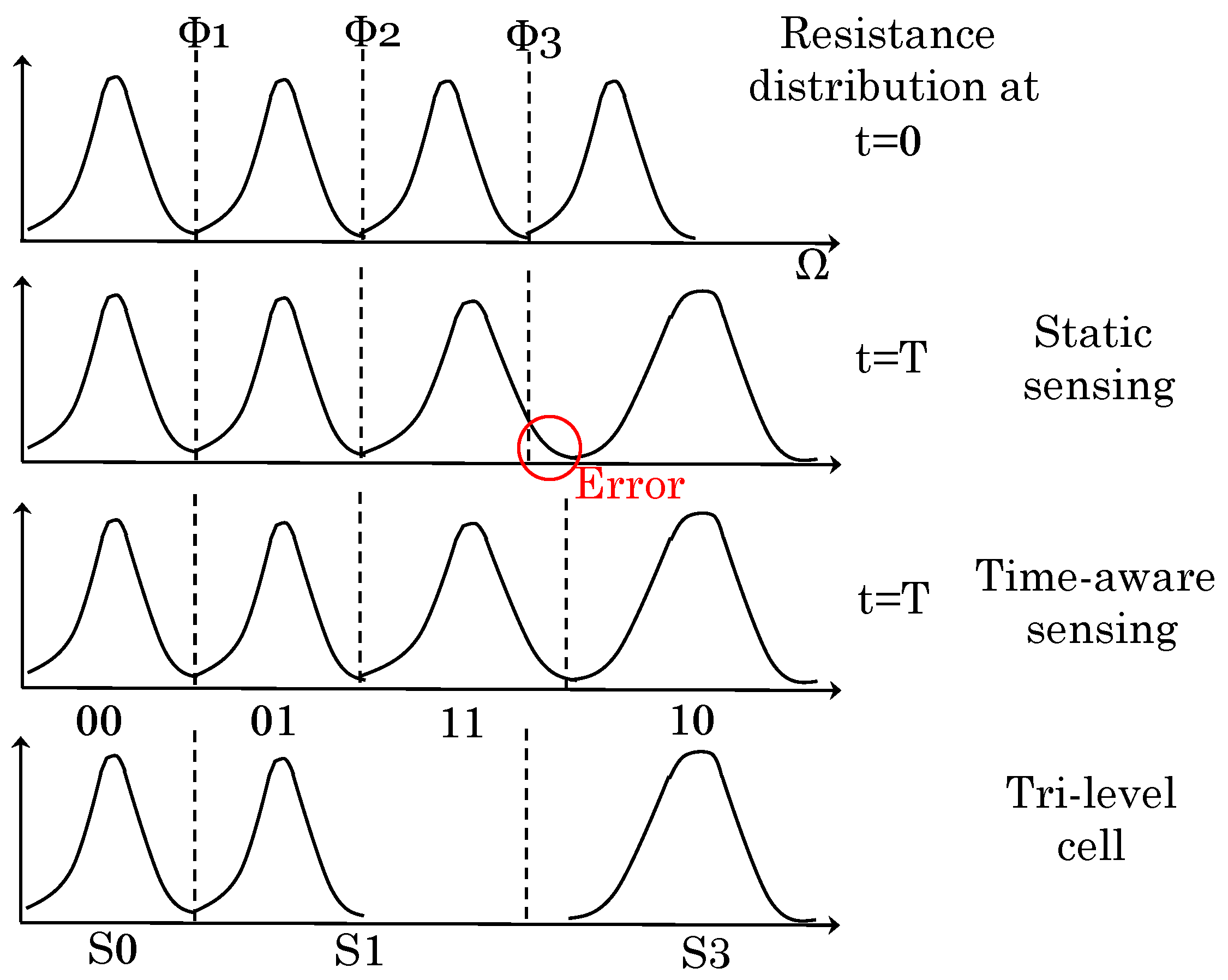
MLC PCM represents data using non-stable states (e.g., semi-amorphous). Due to this, cell resistance increases with time, and the levels with higher initial resistance show a larger amount of drift [13]. If cell resistance reaches that of the next level, the value read from the cell may be different from that originally stored, and thus, drift can lead to errors (refer to Figure 2). A rise in temperature, e.g., due to 3D-stacking, further increases the drift errors [17,18].
We now discuss some simple techniques to address drift errors.
  • To correct drift errors in MLC PCM, scrubbing can be used. In DRAM, different bit errors happen independently, and hence, the probability of multi-bit errors is small. Due to this, even simple scrub schemes suffice for DRAM and incur very low overhead, for example one read and write needs to be issued only once every 200 K cycles [16]. However, in MLC PCM, if one cell drifts to the incorrect state, other cells are also highly likely to drift in the near future. Due to this correlation, multi-bit errors are much more likely in MLC PCM, and hence, a simple scrub scheme would need to read PCM in almost every cycle to keep the error rate at an acceptable level [2,16]. Furthermore, scrubbing leaves very little bandwidth for useful operations. Further, reducing the capacity of MLC PCM to reduce the scrubbing rate is infeasible since the memory capacity becomes too small to be useful [2].
  • In MLC PCM, the resistance margins between consecutive levels increase exponentially, for example when the ratio of consecutive resistance values is five (i.e., R 00 / R 01 = R 01 / R 10 = R 10 / R 11 = 5 ), data remain valid for two years; however, if this ratio is two, the data remain valid for 1 h only (assuming room temperature) [17]. Thus, a simple strategy to address drift errors is to widen the resistance margin between neighboring states. This, however, requires increasing the resistance of the largest resistance states [17], which degrades endurance and energy efficiency due to the requirement of increased programming current. The write endurance of MLC PCM is much smaller than that of SLC PCM ( 10 5 vs. 10 8 writes), and drift mitigation mechanisms may further aggravate the endurance issue [3,16,17], for example due to scrub operations or increased resistance margins.

2.4. PCM Write Disturbance Error

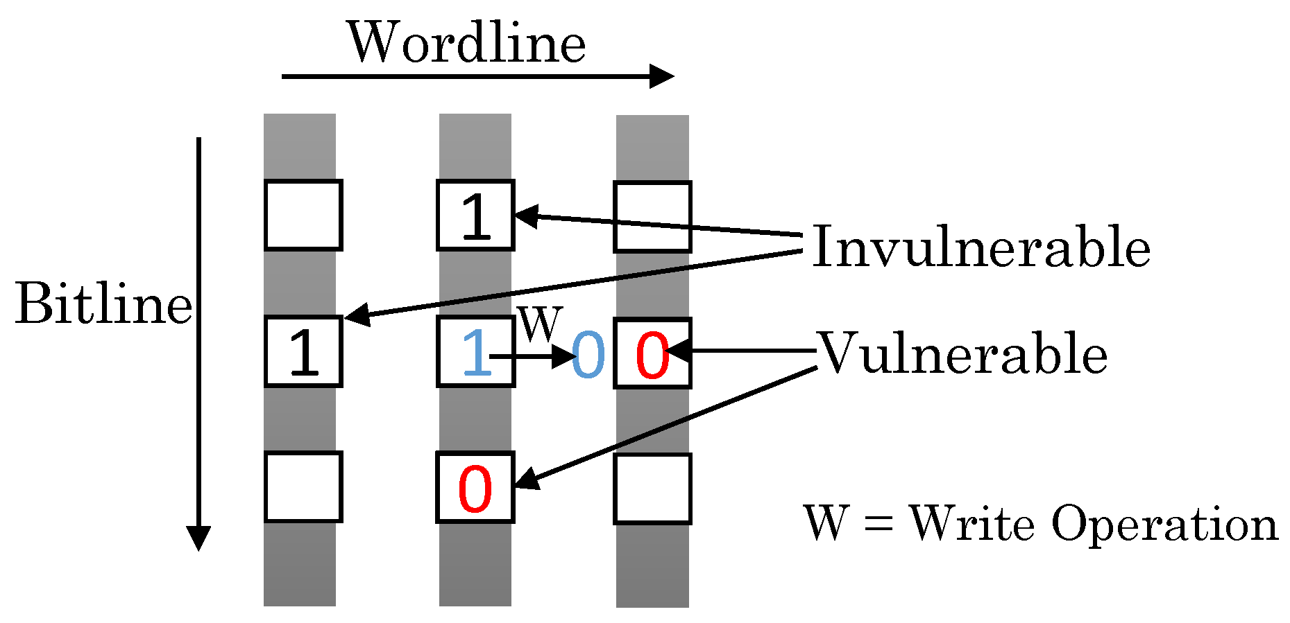
To SETa PCM cell, the temperature is kept higher than crystallization temperature (∼300 C), but lower than melting temperature (∼600 C) for a large time duration. To RESETa cell, it is heated above melting temperature and rapidly quenched. Thus, the heat produced for writing one cell can propagate and change the resistance states of adjacent cells, and this is referred to as WDE. If a cell is being RESET, an adjacent idle cell with a value of zero is vulnerable [22,23], and thus, WDE is a data value-dependent error. The WDE phenomenon is illustrated in Figure 3. Since the SET current is nearly half of the RESET current, WDE due to the SET operation is negligible [3]. WDE is becoming increasingly severe with decreasing feature size, especially at the sub-20-nm node [24].
Some simple schemes to address WDE are as follows:
  • Increasing the inter-cell space reduces WDE; however, it nullifies the density advantage of PCM [22].
  • Since WDE only happens in adjacent idle cells of a cell being written, another approach involves ascertaining all of the vulnerable cells and writing them irrespective of whether their values are changed [3]. However, since PCM has high write latency/energy and a short lifetime [25], this approach leads to very high overhead.
  • The third approach, termed verify and correct (VnC), checks both the written cell and neighboring cells and performs RESET operations where required. However, VnC causes large performance loss [26]. Furthermore, since WDE affects nearby cells (and not the cell being written), performing VnC can disturb other cells, leading to cascading errors.

2.5. STT-RAM Data Storage Mechanism

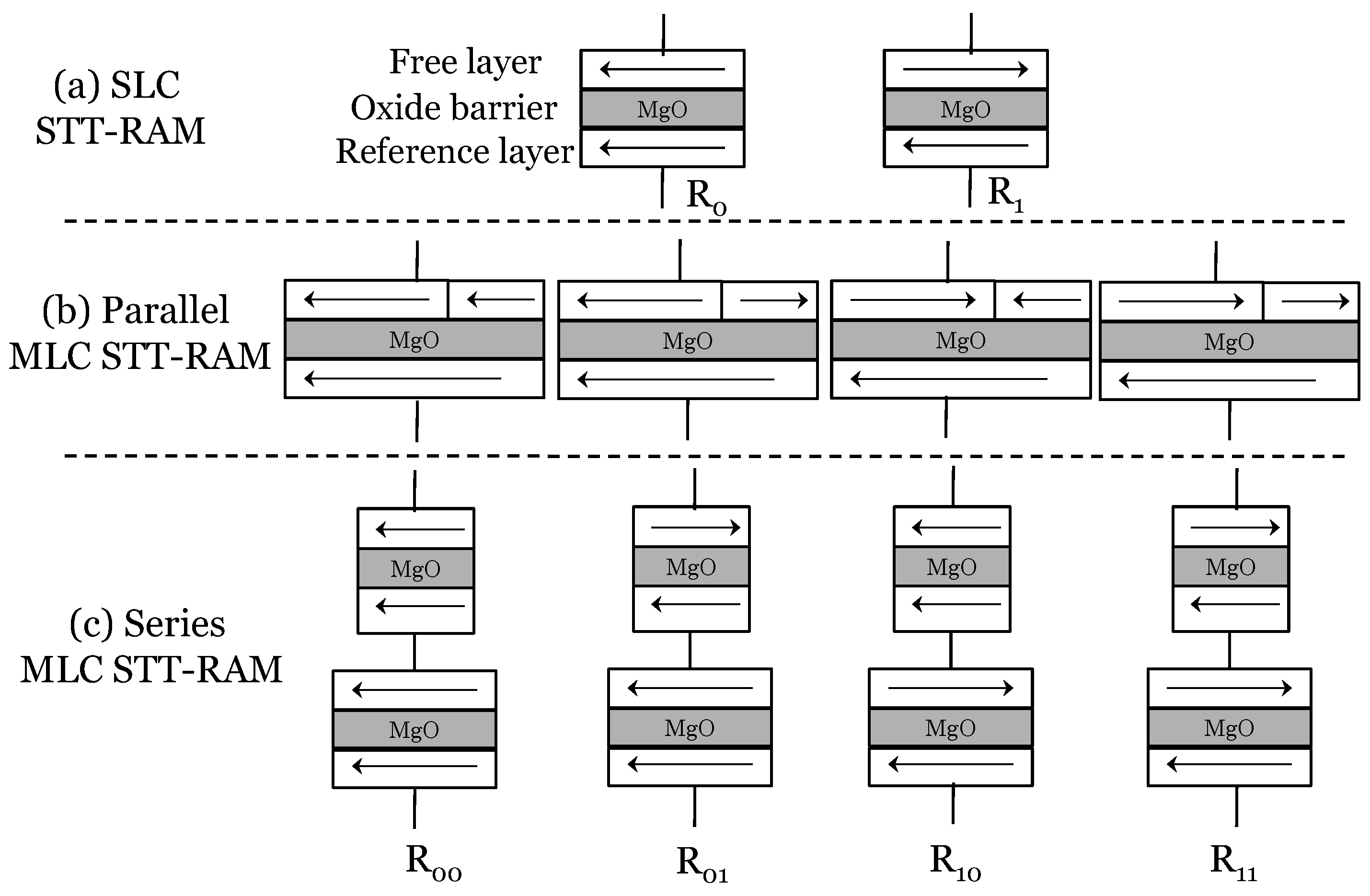
STT-RAM uses an MTJ for data storage, which contains two ferromagnetic layers [27,28,29], as shown in Figure 4a. The magnetic orientation of one layer is fixed, whereas that of the second layer can be changed by applying a current. MTJ resistance is low when these two layers have the same orientation and high when these two layers have different orientations, and thus, the relative magnetization orientation of two layers determines the resistance of MTJ. MLC STT-RAM can be designed in two ways [30]. In the “parallel MTJs” design, the free layer is partitioned into soft and hard domains, each of which can store a bit (Figure 4b), and in the “series MTJs” design, two MTJs with disparate characteristics are vertically stacked (Figure 4c). The parallel MLC has a smaller write current and area, but also has a higher error rate than series MLC [30].
There are multiple strategies for mapping data to MLC memory (refer to Figure 5).
  • Direct (or naive) mapping: An N-byte block can be stored in N / 2 MLC STT-RAM cells, such that even bits are stored in soft-bits and odd bits stored in hard-bits. This cache line is referred to as the mixed line. This has the disadvantage that for any access, both soft and hard-bits need to be accessed, and hence, a two-step read/write is required.
  • Interleaved mapping: The least-significant bits (LSBs) are stored in soft-bits, and most-significant bits (MSBs) are stored in hard-bits. This allows accessing LSBs with smaller latency. The limitation of interleaved mapping is that it requires additional circuitry to regenerate the original data.
  • Cell-split mapping: Two N-byte blocks are stored in N MLC cells, such that one block is stored entirely in soft-bits and another block is stored entirely in hard-bits. Since only one-step read/write is required for accessing soft-bits, this strategy provides better performance if hot data blocks can be mapped to soft-bits.

2.6. STT-RAM Read Disturbance Error

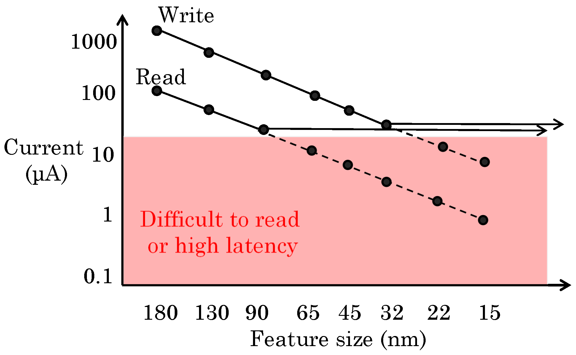
In STT-RAM, feature size scaling has led to a reduction in write current; however, read current has not reduced as much since the correct data may not be sensed on using low-current value [31], as shown in Figure 6. At a large feature size (e.g., 130 nm), read current is much lower than the write current; however, for sub-32-nm nodes, the read current approaches so close to the write current that a read may alter the stored value, and this is referred to as RDE. RDE is data dependent, e.g., using the read current from BL to SL disturbs cells storing “1” only and not “0”. Even with strong ECCs, the RDE rate at small feature sizes can exceed that acceptable for on-chip caches [4]. In STT-RAM, reads and writes cannot be independently optimized, e.g., reducing the MTJ thermal stability for improving switching performance increases the probability of read disturbance, and thus, RDE mitigation involves tradeoffs. For these reasons, RDE is expected to become the most severe bottleneck in STT-RAM scaling and performance [4,32].
Some simple strategies for addressing RDE are discussed below.
  • The margin between read and write currents can be increased by increasing the write current; however, this will further increase the already high write power of STT-RAM.
  • To address RDE, low-current sense amplifiers can be used, which have a larger sensing period. This approach does not create RDE, but may increase sensing latency by three times [33,34], which harms performance.
  • Since after a read operation, the data value is stored in sense amplifiers and remains free of RDE, a third approach consists of writing this stored data value back to STT-RAM cells, and this is referred to as the restore/refresh-after-read [4,31] or high-current restore-required (HCRR) read approach [34]. However, these restore operations consume bandwidth and reduce cache/memory availability. Furthermore, this scheme does not leverage the properties of the data value (e.g., zero data) and cache access behavior to avoid unnecessary restore operations.
  • By reducing the number of reads/writes from STT-RAM cache by techniques such as cache bypassing [35], both RDE and write errors can be reduced [6].
  • A recently-proposed magnetic RAM, named SOT-RAM (spin orbit torque RAM), does not suffer from RDE [36], and hence, this can be used as an alternative of STT-RAM.

2.7. STT-RAM Write Errors

In STT-RAM, a write operation may not succeed due to the stochastic switching characteristics of MTJ, and this leads to write errors. Furthermore, the error rate of the 0 1 transition is significantly higher than that of the 1 0 transition [37]. The error probability can be reduced by using a large duration and magnitude of the write pulse; however, due to parametric variations, precise control of these is challenging [30].
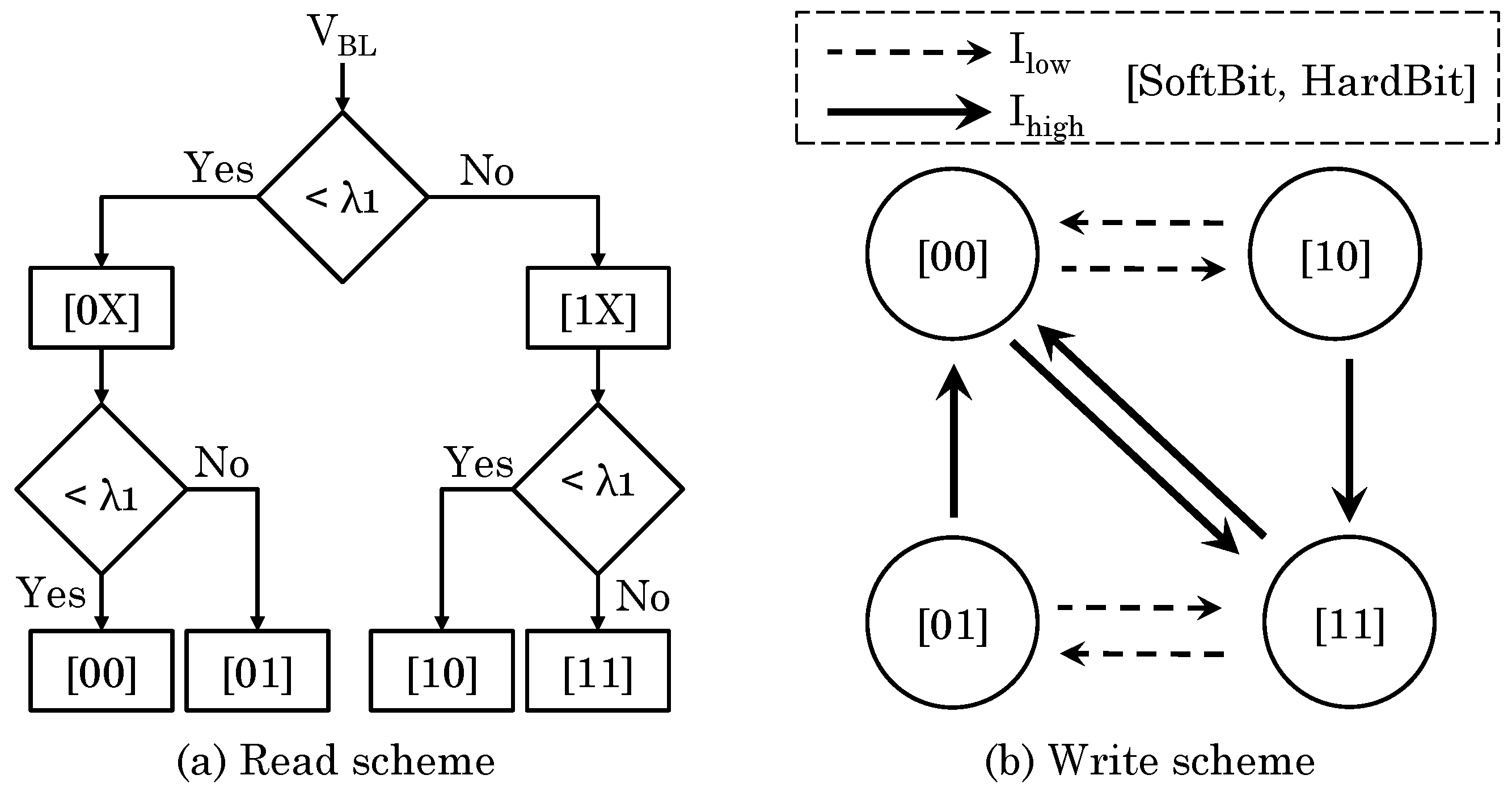
Writing an MLC STT-RAM may require one or two steps, as shown in Figure 7. For writing 00 or 11, a high current is applied to change both soft- and hard-bits. For writing 01 or 10, in the first step, a high current is applied to write 00 or 11, and in the second step, a low current is applied to only change the soft-bit. This write scheme can show two types of errors. First, on writing the soft-bit, the hard-bit may also get written, which is called “overwrite” error. Second, if the write current is not sufficient to change the soft-bit, “incomplete write” error occurs. On changing both bits (Step 1), only incomplete write error can happen; however, on changing only the soft-bit (Step 2), both kinds of errors can occur. Simple strategies for addressing write errors include ECC and repeatedly performing VnC operations, and their limitations have been discussed above.
Table 1 summarizes the characteristics of different errors. Clearly, due to the differences in the behavior of these errors, unique architecture-level techniques are required for mitigating them.
These NVMs show a few other types of errors, as well. For example, compared to SLC STT-RAM, MLC STT-RAM uses a narrow resistance margin. Due to this, adjacent states show overlap [30], and hence, an incorrect value may be read, leading to read errors. Similarly, the stochastic bit-flip due to random thermal fluctuation can lead to retention failure in STT-RAM [27,36]. Furthermore, a decision failure occurs when the datum stored is incorrectly sensed on a read operation.

3. Classification and Overview

Table 2 organizes the works based on the memory technology, cell-type (SLC/MLC) and reliability issues addressed by them. Table 3 classifies the works based on processing unit, processor component and their figures of merit. Due to their high density and low leakage, NVMs are primarily beneficial for large capacity storage structures, such as caches and main memory in CPU and RF (register file)in GPU. Hence, most works have addressed these components. Since the first and last level caches have different characteristics and optimization targets [32,38], the table also classifies the works based on this factor. Since reliability improvements may be achieved at the cost of performance and power, many works analyze the performance/energy impact of their technique, and this is also shown in the table.
Table 3 also classifies the works based on their key ideas and management approaches. We now comment on these and other key ideas.
  • Both ECC and data-duplication approaches increase the redundancy for enhancing reliability.
  • In MLC PCM and MLC STT-RAM, some states show higher error rates than others (refer to Section 4.1 and Section 7.1). Hence, some works use the partial data mapping approach to avoid error-prone states. An example of this is ternary coding, where only three out of four states in a two-bit MLC are used for storing data. The limitation of partial data mapping, however, is that it may require additional conversion steps, since other processor components may still use binary coding. Other schemes to avoid error-prone or vulnerable states include bit-inversion and bit-rotation. A limitation of data-dependent techniques, such as rotation and inversion, is that they may not work well in the presence of random, encrypted or compressed data.
  • Some works propose techniques based on asymmetric error rates of 0 1 and 1 0 transitions.
  • Some works use different data-encoding schemes than the traditional binary encoding. For example, partial data mapping techniques may use ternary encoding, and some works use Graycoding to reduce the number of bit transitions. A few works use WOM (write-once-memory) codes [48].
  • Some works use data compression [53] for various optimizations, e.g., to make space for storing ECC [3] or for performing duplication [39], to compensate capacity loss due to partial data mapping [3], to facilitate switching from MLC to SLC mode [49] and to reduce the number of bits vulnerable to RDE [39] and WDE [26]. The efficacy of these techniques, however, depends on the compressibility of data.
  • Some works perform VnC (also called write-read-verify) operations to reduce the error rate in write operations. Others perform scrubbing (which resembles DRAM refresh) to address PCM drift errors. The difference between these is that VnC is generally performed immediately after a write operation to remove the errors in the write operation, whereas scrubbing is performed periodically at idle times to remove the errors accumulated after a write operation. Furthermore, the scrubbing scheme reads and writes the same data assuming that stored data are correct, whereas the VnC scheme checks for the correctness of stored data and, in the case of errors, issues further writes.
  • Some techniques combine multiple resilience strategies to lower their individual overheads. For example, on using VnC with ECC, VnC steps can be stopped once the number of errors is within the correction capability of ECC, which reduces VnC overhead. Similarly, the error rate reduction brought by VnC allows using an ECC with a lower error correction capability, which reduces ECC overhead.
  • Some techniques predict cache/RF read/write intensity or reuse distance [4,6,43]. This information can be recorded using a compiler [43] or hardware [4,6].
  • Some techniques use ECCs with different correction capabilities to deal with different error rates [6,20,40,41,52].
  • Some techniques hide the latency of WDE correction [22] by storing this in a buffer and scheduling it later when the cache or main memory is idle.
  • Due to the limited write endurance of PCM, many PCM management techniques account for its endurance, as well [13,17,18,21,47,50,51,52].
  • A few other management techniques include early write termination [30,37], changing the operational mode of STT-RAM at runtime [32], cache bypassing [6], page remapping [23] and using data migration in the cache [6].

4. Addressing PCM Resistance Drift Errors

Since drift depends on time elapsed and temperature, some works perform PCM reads in a time-aware [13,18,19,20] and a temperature-aware [18] manner, which involves changing threshold resistance based on time and/or temperature (refer to Figure 2). Some works statically divide the resistance spectrum such that larger margins are used for states with a higher drift rate [21,50]. Some works perform memory page allocation in a temperature-aware manner [17], whereas others perform the runtime transition of a memory page or a cache block between drift-prone MLC and drift-free SLC [17,49]. We now review some of these works.

4.1. Partial Data Mapping

Seong et al. [2] note that in a four-level cell (4LC) PCM, one of the four levels shows the highest resistance drift. They present a three-level cell (3LC) PCM, which removes the most error-prone level and, thus, reduces the errors caused by this and the nearby level. For utilizing 3LC, they propose schemes to convert between a binary and a ternary number system. They show that compared to 4LC, 3LC reduces the error rate by five orders of magnitude and achieves 1.33× higher density than SLC PCM. In fact, since 4LC would require very strong ECC with many redundant bits, 3LC can achieve higher density than even 4LC. Furthermore, the soft-error rate of 3LC is smaller than that of DRAM without requiring scrubbing or ECC. Further, the performance with 3LC is much higher than that with 4LC and close to that with SLC.
Yoon et al. [21] discuss the 4LC-PCM architecture for achieving acceptable error rates. For a 16-GB 4LC-PCM memory, they suggest refreshing each bank independently with a refresh interval of 2 10 s (17 min), which provides 97% bank availability and is over double the time required to refresh the entire memory. Further, since the frequency of the occurrence of four states is different in typical applications, they propose mapping two less frequent states to two error-prone levels (01 and 10). Furthermore, they propose increasing the resistance margin at the amorphous side and reducing it at the crystalline side, which reduces drift errors. Using these two optimizations with a 10-bit correcting ECC and 17-min refresh allows keeping the error level acceptable for a practical system. However, even with these optimizations, 4LC has a high error rate and large performance overhead, and hence, they propose removing the most error-prone state to achieve a 3LC design. 3LC requires no ECC or refresh for 16 years. They store three bits in two 3LCs, which has a density of 1.5 bits/cell. Since two 3LCs have nine levels, of which only eight levels are used to encode three bits, one level remains free. This level is used as a spare when a cell reaches its endurance limit (refer to Table 4), and this allows tolerating hard errors. This along with simpler ECC (due to the low error rate of 3LC) allows 3LC to achieve density close to that of 4LC. They show that their 3LC design provides higher performance and lower energy consumption than the 4LC design.

4.2. Selectively Using SLC Mode

Zhang et al. [17] present a drift-resistant PCM architecture. They note that in the four-level PCM, states 00 and 11 are drift-resistant, 01 is less prone to drift and 10 is most prone to drift. Hence, they selectively use bit-inversion, -rotation or both to store most of the values in 00 or 11 patterns, instead of 01 or 10 patterns. Bit-inversion is useful for changing the pattern from 10 (high-drift) to 01 (low-drift). Rotating for an odd number of times can change the state to the low-drift or drift-resistant state, e.g., rotating 0110 once gives 0011, where 00 and 11 are drift resistant. These strategies are illustrated in Figure 8.
Further, since SLC PCM does not suffer from drift, their technique allows switching from MLC to SLC at page-granularity when PCM shows drift-sensitive behavior. SLC pages do not require rotation/inversion, and their lower error rate partially offsets the performance loss due to reduced capacity. Since drift is strongly impacted by temperature, the page allocation mechanism observes the temperature of memory portions and preferentially allocates pages from lower temperature portions. Furthermore, MLC and SLC pages are mapped to low and high temperature portions, respectively. Compared to the scheme of increasing resistance margins to address drift, their technique brings a large reduction in the error rate.
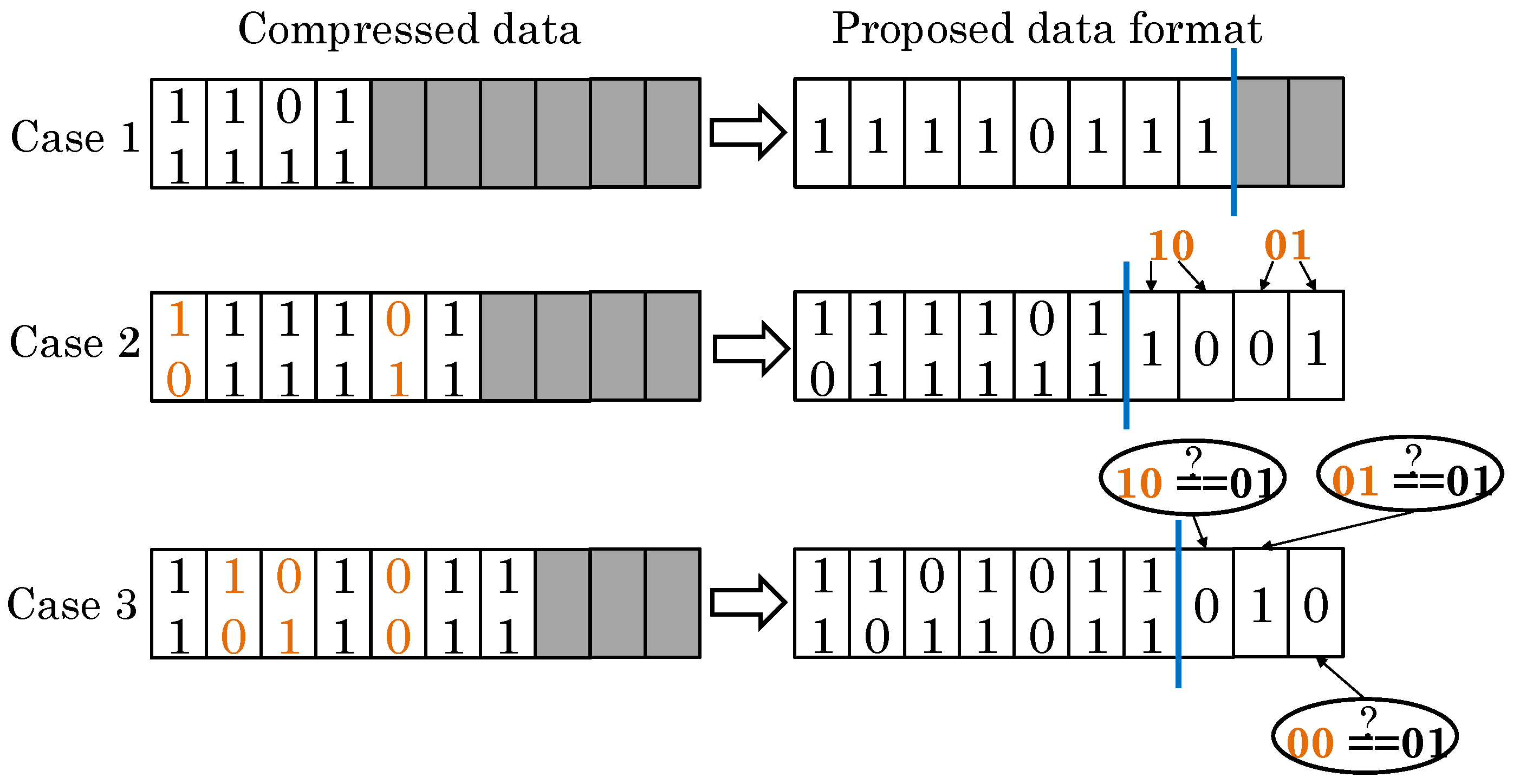
Jalili et al. [49] present a drift-mitigation technique that works by converting drift-sensitive blocks to drift-immune blocks. Their technique uses data compression and selectively switches between MLC and SLC modes since SLC is drift free. Based on the width of compressed blocks, three cases arise (refer to Figure 9). In Case 1, the compressed block has less than 50% of the original size, and hence, it is stored in SLC mode, which provides reliability and performance benefits. In Case 2, the compressed width is greater than 50%; hence, pattern 11 is removed from the compressed stream since 11 is drift resistant. Then, the compressed block is stored in MLC, and the compressed block with the omitted 11 pattern is stored in SLC mode. Thus, only drift-sensitive patterns are backed up in SLC mode. In Case 3, the compressed width is even larger than that required in Case 2. In this case, the compressed block is stored in MLC. Furthermore, the 11 pattern is removed from the stream and the beginning with the right most cell of SLC, a cell is set for the error-prone 01 pattern and reset for the 00 and 10 patterns. At the time of reading, for Case 2, the 11 pattern is removed from the compressed stream, and the remaining pattern is compared against its backup in SLC. Since Case 3 is not an error-free formation, after performing a check along the lines of Case 2, ECC also needs to be checked to detect any errors. Their technique reduces the error rate while improving the performance and energy efficiency.

4.3. Non-Uniform Partitioning of the Resistance Spectrum

Asadinia et al. [50] note that traditional MLC PCM devices divide the resistance range uniformly. Although this reduces the maximum read latency, it leads to equal energy/latency for all of the states. To address the drift issue and also improve performance, they propose dividing the large resistance range of PCM in non-uniform regions having different read/write energy and latency, and thus, the resistance margins are contracted or expanded. The access latency of the most expanded region (close to fully amorphous) is one cycle, while that of the most contracted region (close to crystalline) is slightly higher than that in traditional MLC. Further, since few data patterns occur with much higher frequency in applications than other patterns, their technique maps these frequent patterns to low-latency/energy states. This improves performance and energy efficiency. The decision to use non-uniform or uniform division is taken based on the value locality characteristic of the application. Further, by virtue of using a larger margin at the amorphous end and a smaller margin at the crystalline end, their technique reduces errors due to drift, since states closer to the amorphous end are most prone to drift. Compared to traditional PCM, their technique improves the PCM lifetime, performance and energy efficiency and achieves the same error rate at a lower energy overhead.

4.4. Performing Reads in a Time- and Temperature-Aware Manner

Xu et al. [13] propose a time-aware PCM read technique to address PCM drift. Their technique records the time duration for which the data value is stored in the PCM cell. At PCM read, this time duration decides the quantization and interpretation of the cell resistance. They show that their technique improves MLC PCM reliability significantly, and on using BCH and LDPC (low-density parity check) codes, the time duration, for which data can reside in PCM while the drift error rate still remains acceptable, increases by four and seven orders of magnitude, respectively.
Liu et al. [19] note that time-aware PCM read schemes (e.g., [13]) ignore the inter-cell age variations, and hence, for cells written a long time after the oldest cell was written, these techniques record the resistance incorrectly. They present a technique that also accounts for both inter-cell and intra-block variations in age to achieve a high accuracy of quantization. The time-aware technique [13] uses the ages of the oldest level k cell and the oldest level k + 1 cell for computing the quantization threshold between levels k and k + 1 (where 1 k N , N = 4 for 4LC), whereas their technique uses the ages of the oldest level k cell and the youngest level k + 1 cell. Further, for reducing the quantization error of cells read soon after being written, an adaptive writing scheme is used. If a cell is written much later than the time the corresponding block is created, the reference resistance does not remain fixed, but is increased to allow a sufficient quantization margin for recently-written cells. Their technique brings a significant reduction in the quantization error rate.
Jalili et al. [18] propose performing PCM read operations in a time- and temperature-aware manner for tolerating drift errors instead of correcting them by ECC. They use PCM as a 3D-stacked memory where the operating temperature is even higher than that in 2D memory. In their technique, at the time of PCM write, the current time is also recorded with the block. At PCM read, the memory controller determines the extent of drift based on the time elapsed and temperature. They note that on using narrow resistance margins, drift has no impact on a large fraction (e.g., 60%) of memory accesses, and this also saves write energy. However, for remaining cases where the elapsed time, or temperature, or both are high, margins cannot avoid the drift errors. To address them, the reference voltage of the read-circuit is updated to account for drift. For this, they use an analytical model for predicting drift behavior for a given temperature, elapsed time and initial resistance. Using this model, the PCM read circuit estimates the resistance drift and calibrates the threshold voltage for adaptively sensing the state of the cell. Thus, their technique interprets the cell state in a dynamic manner. They show that their technique reduces the PCM error rate by six orders of magnitude.

4.5. Using Error Correction Strategies

Yang et al. [20] propose techniques to address drift errors in MLC PCM. They note that drifts from 10 to 01 and 01 to 00 lead to soft-errors and 00 to 01 lead to hard-errors (since the cell gets stuck at a value and can no longer be written). They use Gray coding, which maps 11 to 10 and 10 to 11 (the mapping of 00 and 11 is not changed). This changes the 10 01 drift to the 11 01 drift. Then, two-bit interleaving is used to store left-side and right-side bits of two-bit cells separately. Due to this interleaving, the data in left-side bits show a low error rate, and hence, only simple ECC (e.g., Hamming code) is used for them. The data in right-side bits show a much higher error rate, and hence, stronger ECC (two error correction) is used for them. For the right-side bits, they partition the block at sub-block granularity and store the data in inverted form to address stuck-at-fault (hard) errors. They also tune threshold resistance to lower hard- and soft-error rates even further. They show that for a desired data retention time and number of programming steps, an optimal value of the threshold resistance exists. Using all of the techniques together brings a large reduction in the error rate, which allows using simpler ECC for the same reliability and the same ECC for even stronger reliability.
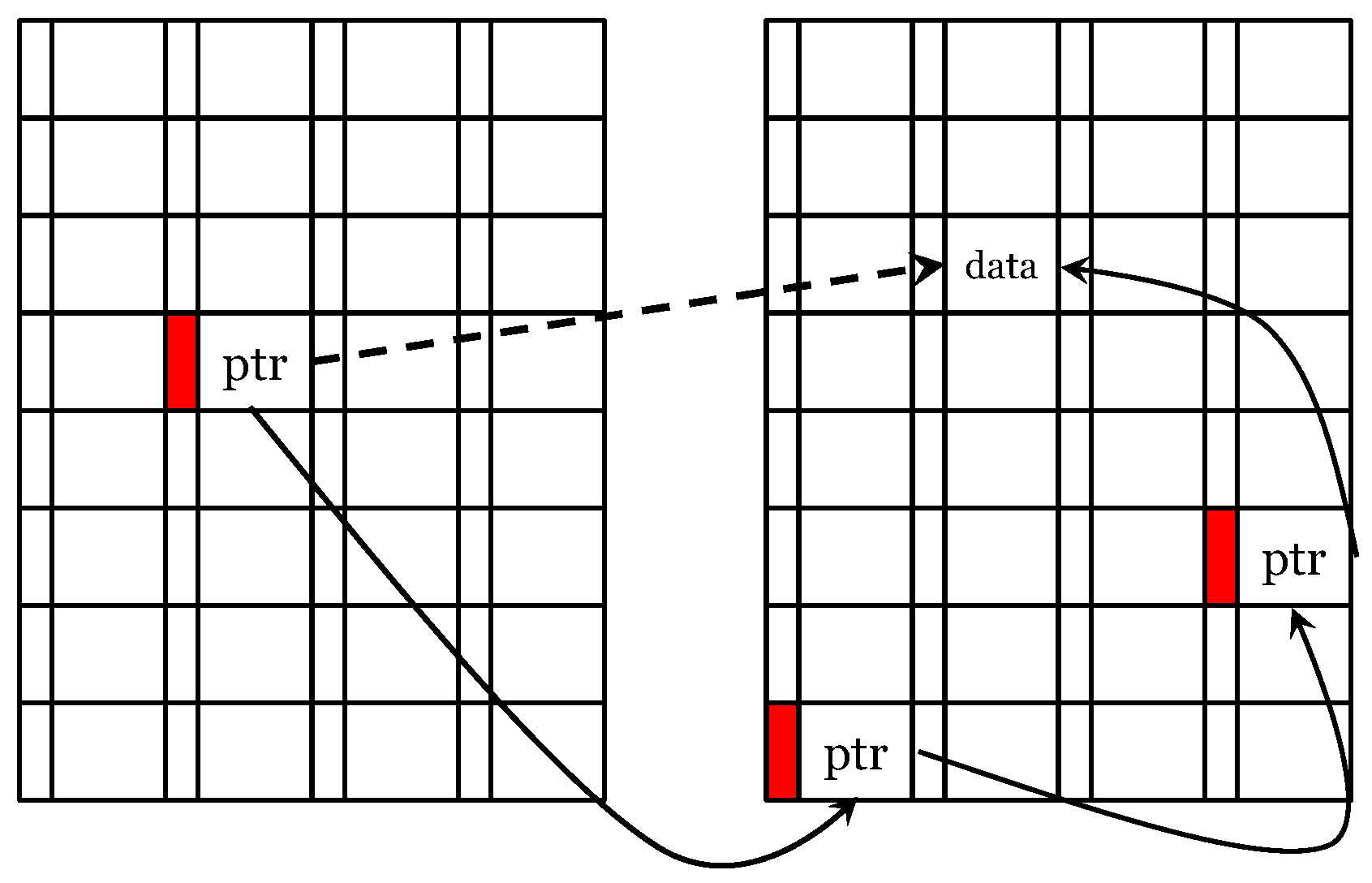
Yoon et al. [52] present a technique to protect NVMs against both soft- and hard-errors. In the conventional coarse-grain remapping technique, the failure of even one cache block leads to remapping or disabling of a 4-KB page. In their technique, when the number of errors in a 64-B block exceed the correction capability (four bits), only this failed block is remapped. Further, they use the healthy cells of worn-out blocks to record the redirection address. To avoid chained remapping on failure of a remapped block, the final address is stored in the original failed block itself (refer to Figure 10). To reduce the latency of accessing remapped data, remapping pointers are stored in a cache.
They use a 6EC7ED (6-bit error-correction 7-bit error-detection)BCH code and use it for tolerating initial wear-out errors. They further note that a bit wears out in a long time, but after it wears out, it may always provide incorrect data. By comparison, soft-errors happen rarely. Based on this, they use simple ECC for most blocks with little or no errors and strong ECC for blocks with multi-bit errors. They use three ECC schemes: fast, slow and memory-ECC. Fast-ECC detects at most seven errors, but corrects at most two errors, and thus, it handles two wear-out errors in a block. If fast-ECC detects more than two errors, slow-ECC is used, which corrects at most four errors, and for more errors, memory-ECC is invoked. Mem-ECC can correct at most six errors, and it ascertains whether an error is a wear-out error by writing and verifying the data. On detecting five or a higher number of errors, the failed block is remapped, which avoids the need for calling memory-ECC again for this block. Their technique improves NVM lifetime significantly and incurs only a small performance loss.

4.6. Using Scrubbing

Awasthi et al. [16] present scrub mechanisms to address the drift issue in MLC PCM. For an ECC code that can correct K errors, performing a scrubbing operation after K errors, but before the occurrence of the K + 1 -th error can protect the data. They observe that with increasing the K value, the time difference between the K-th and K + 1 -th error also increases, and hence, they propose using multi-bit ECCs, which allow using larger scrub intervals. They further propose improvements to simple scrub schemes. For instance, if the K + 1 -th error happens quickly after the K-th error, the data cannot be corrected. To avoid this, they propose a “headroom” scheme, where a scrub operation is issued on detecting K - h errors (instead of K errors), where h shows the headroom. However, scrub operations lead to extra writes, which increase the hard error rates due to the small write endurance of PCM. Hence, the value of h can be intelligently chosen to balance uncorrectable soft-error rates and hard-error rates. Their second scheme works by increasing the frequency of read (for drift detection) operations gradually as a larger number of drift-errors is encountered since the lines with very few errors are not expected to require correction. The third scheme uses adaptive scrub-read rates, such that after each interval of P writes, the uncorrectable errors in the previous interval are examined, and the rate is doubled if errors exceeded a threshold. They show that compared to a simple scrub scheme, their technique brings significant reduction in uncorrectable errors, scrub-related writes and scrub energy.

5. Addressing PCM Write Disturbance Errors

We now discuss techniques for addressing WDE. These techniques mitigate WDE along the word-line [3,26,48] or bit-line [22,23,48]. Some techniques specifically mark a few blocks as unused, which avoids the need for correcting WDE in them [22,48].

5.1. Using the Data-Encoding Scheme

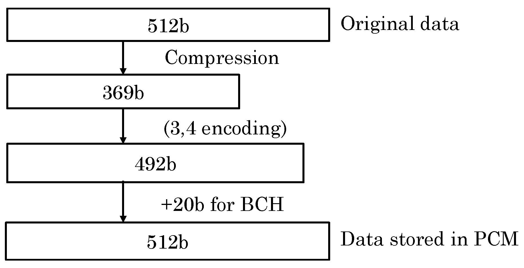
Jiang et al. [3] propose a technique to address WDE in SLC and MLC PCM. They assume that the inter-cell distance along BL is large enough, whereas that along WL is reduced, and thus, WDE happens only along WL. Their technique attempts to compress a block. Assuming a 64-B (512 b) block, if it can be compressed to at most 369 bits, the compressed block is encoded using (3,4) encoding (explained below), which requires at most 492 bits. Then, the 20-bit 2EC3ED BCH code is added for protecting the encoded pattern, as shown in Figure 11. An uncompressed block is not encoded. While writing an encoded block, their technique checks the number of WDEs and completes a write if at most two WDEs are present (since the BCH code can correct two errors), otherwise, it attempts VnC. While writing uncompressed block, the write terminates only when no WDE is present.
Their technique uses the ( p , q ) ( q > p > 1 ) encoding scheme, which uses a q-bit code to encode p-bit data (refer to Figure 12). Since this encoding requires a larger number of bits, their technique chooses WDE-resistant codes. They note that since WDE happens only if a nearby cell is zero, out of four two-bit patterns, viz. 00, 01, 10 and 11, the 00 pattern leads to WDEs. Hence, their (3,4) encoding removes eight four-bit patterns with 00 (e.g., 1100, 0011, 0100, etc.) and uses the remaining eight patterns to represent three bits (from 000 to 111). This encoding decreases the frequency of vulnerable patterns, although it cannot remove them entirely. They also propose WDE mitigation strategies for MLC PCM. Their technique mitigates WDE, which allows designing highly-dense PCM chips and also reduces the performance penalty of VnC.

5.2. Consolidating Correction Operations

Wang et al. [22] note that increasing the inter-cell spacing in PCM to address WDE stretches the cell-size from 4 F 2 to 12 F 2 , which reduces the density. They propose a technique to address WDE along BL to allow designing a 4 F 2 cell, which is the minimum size for diode-switch-based PCM. They use the scheme of Jiang et al. [3] to mitigate WDE along WL and, thus, focus on reducing WDE along BL. Furthermore, they use ECP [54] for correcting hard-errors in PCM. The ECP technique works by encoding and storing the addresses of failed cells and allows tolerating errors in memory bit locations by keeping pointers for them and using backup cells for replacement [54]. Wang et al. note that, after applying the scheme of Jiang et al. [3], a PCM block write causes on average only two WDEs in each of its nearby blocks, and hence, immediately correcting them is an overkill on performance. Hence, their lazy correction scheme records error locations and values in ECP and corrects errors only when they exceed the correction capability of ECP. ECP entries are preferentially allocated to hard-errors and then to WDEs. If all ECP entries are used by hard-errors, WDEs are addressed by the VnC scheme. The ECP chip itself is designed using a lower density cell ( 8 F 2 /cell), and hence, writing ECP does not cause cascading WDEs. Lazy correction consolidates multiple correction operations into one, and this correction can even be done by the regular write operation. However, compared to WDE-free PCM, this scheme still requires two extra “pre-write” read operations for storing old data and two extra “post-write” read operations for verification.
To hide the latency of “pre-write” reads, their second scheme issues them when the write request is waiting in the write queue. Since memory controller buffers write and issue them when the queue is full, write requests see a large waiting time, and thus, pre-reads can be issued during this time. To further reduce the impact of WDE on write-intensive applications, they note that VnC is not required for a block flagged as “no-use” by the OS. Based on this, they propose a ( y : z ) ( 0 < y z ) allocation scheme, which uses only y out of z successive strips (rows having the same index from all memory banks) for storing data. For example, the (1:2) scheme uses alternate strips and, thus, requires no VnC at all, whereas the (2:3) scheme requires only one neighboring cell and not both neighboring cells. Thus, the ( y : z ) allocation scheme exercises a tradeoff between memory capacity and performance and can reduce the performance penalty for high-priority applications. Compared to the 8 F 2 /cell WDE-free [3] design, their 4 F 2 /cell design with the proposed techniques achieves significantly larger density. Furthermore, compared to the VnC scheme, their techniques provide a large performance improvement.

5.3. Reducing Correction Overhead on the Critical Path

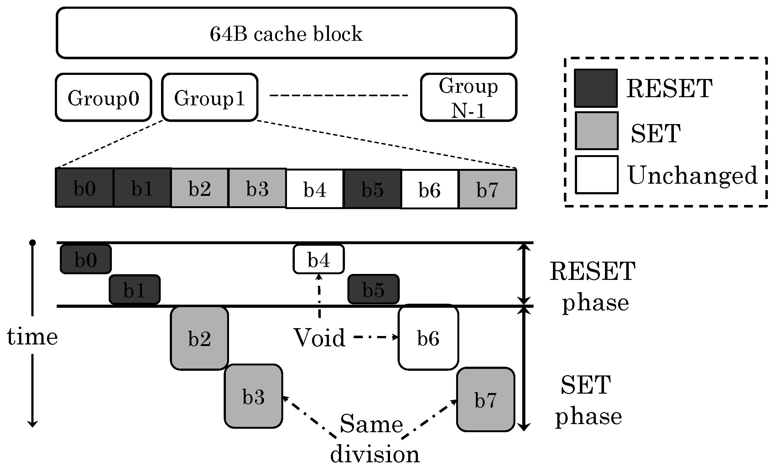
Wang et al. [26] note that since PCM consumes much greater write power than DRAM, PCM writes are performed at the granularity of cell groups. Different cell groups proceed independently. In a group, k-bits can be simultaneously SET or RESET, but not mixed. For example, for k = 2 , bits that are four cells apart can be simultaneously written, and multiple rounds of SET and RESET operations are required to write a cache block. This is illustrated in Figure 13. Thus, the slowest cell group(s), termed as the critical group(s), determines the total write latency. Since the number of critical groups is smaller than that of the non-critical groups, WDEs from critical groups are also smaller, and hence, they can be preferentially mitigated to avoid their performance penalty.
Their technique works separately on each group. In each round of RESET, their technique uses both write-data verification and WDE verification to detect disturbed cells after RESET. Then, their technique ascertains whether correcting the disturbed cells by additional RESET operations will increase the total write latency. If so, this group is a critical group, and hence, the unused ECP [54] entries are leveraged to correct them; and this latency is hidden by overlapping with ongoing RESET/SET rounds. Otherwise, this is not a critical group, and as such, their technique corrects these cells within the cell group before proceeding to the SET round. During a write operation, their technique tries to free some ECP entries if they correspond to WDEs. For further optimization, their technique performs data compression and does not correct the bits of the block that remain unused due to compression. They show that by using only two ECP entries for correcting WDE, their technique almost completely removes the performance overhead of WDE.

5.4. Using Page Remapping Scheme

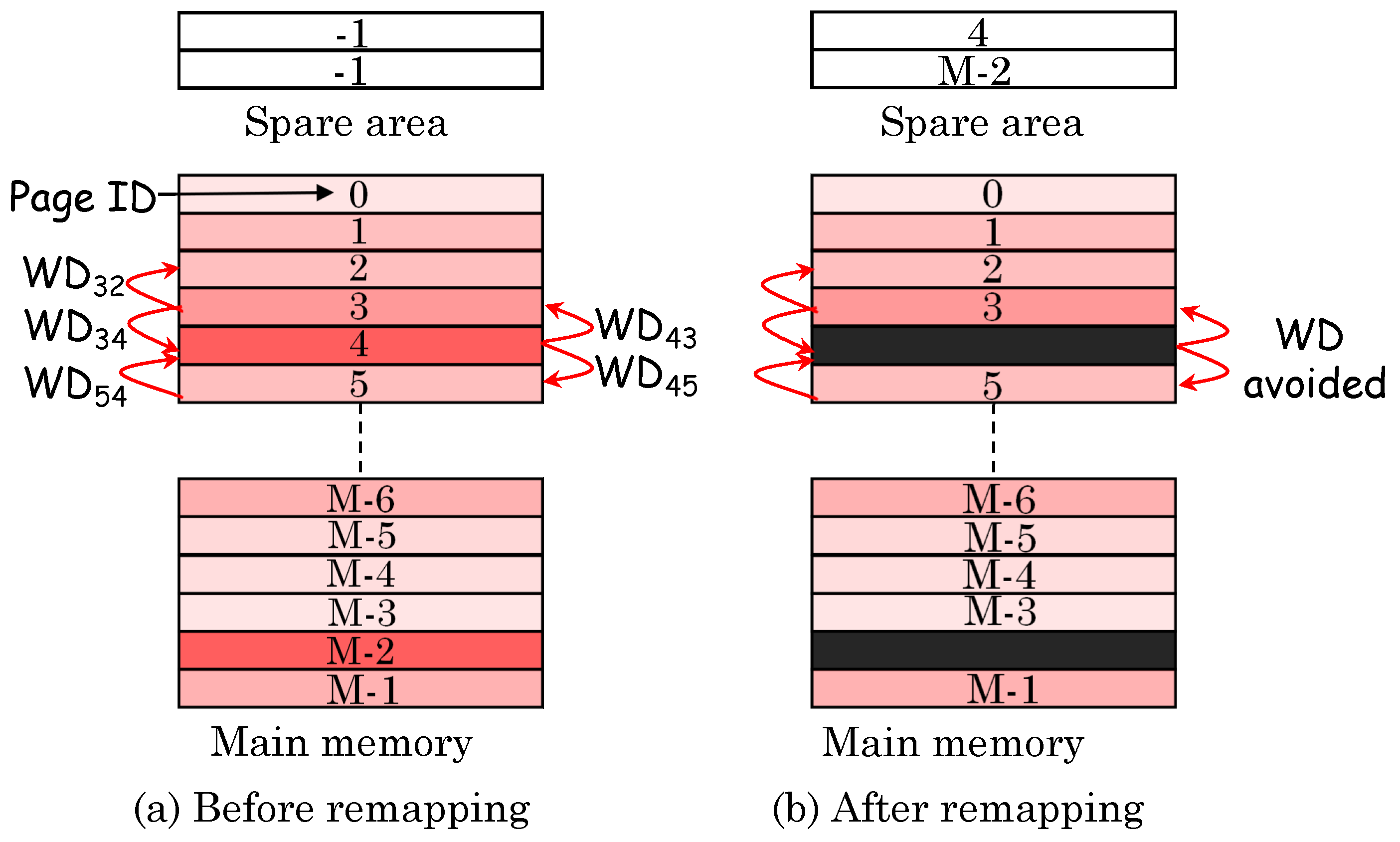
Wang et al. [23] note that since most writes to main memory are directed to a few pages, they are primarily responsible for WD. Their technique works by redirecting such hot pages in a spare area, (1) WD in neighboring pages due to remapped hot pages and (2) WD in hot pages due to neighboring pages being able to both be avoided (refer to Figure 14). Thus, the page remapping approach leads to a two-fold reduction in WDE. Further, by reducing the writes to PCM main memory, their technique also improves the PCM lifetime.

5.5. Using Layout and Coding Schemes

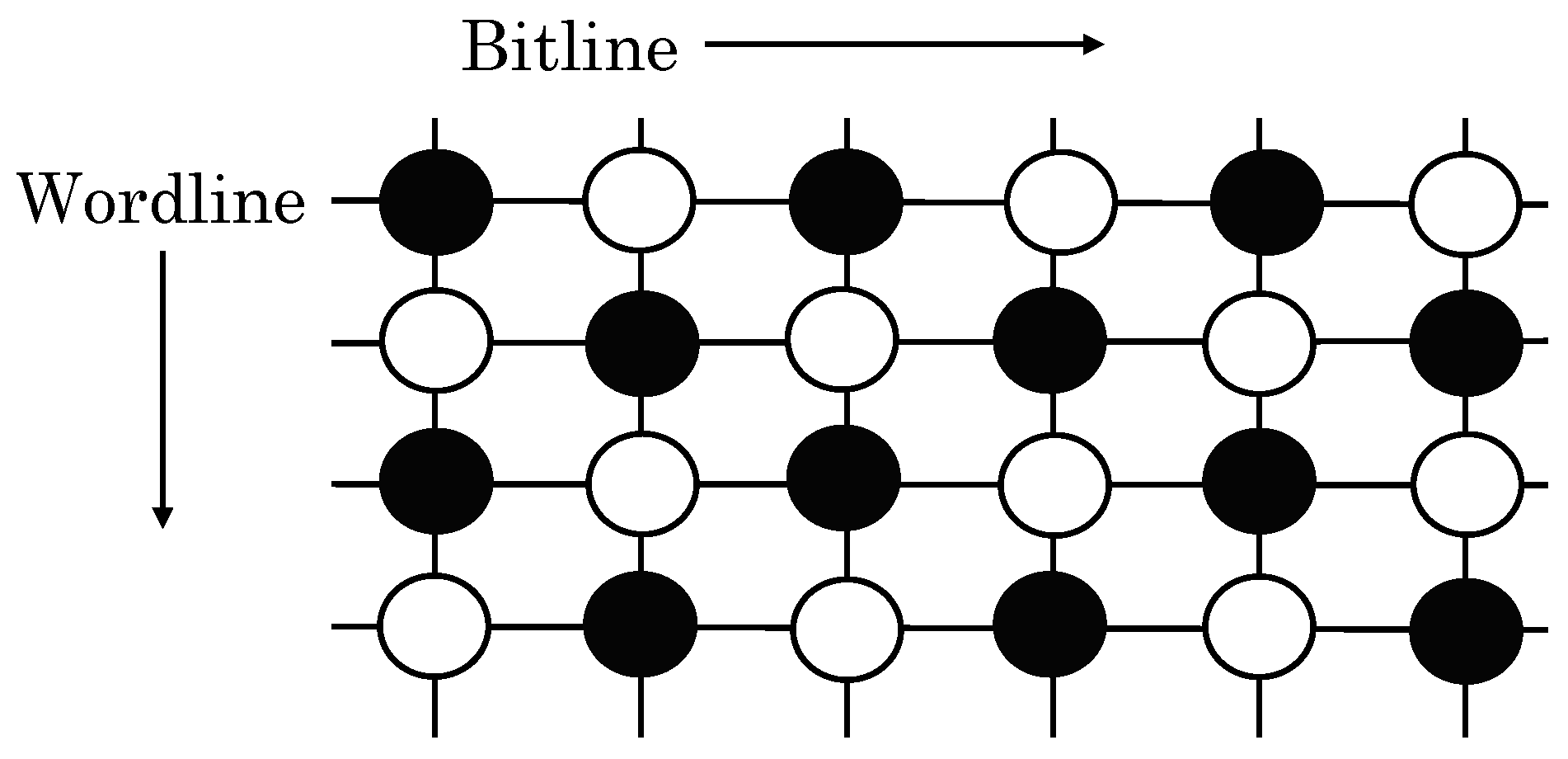
Eslami et al. [48] present the cell layout and coding scheme to mitigate WDE in PCM. They propose a checkerboard layout of PCM cells where nearby cells along BL and WL are designated as white and black, as shown in Figure 15. Only white cells are used first, which avoids the need for correcting black cells. After white cells exhaust their lifetime, they are no longer used, and then, black cells are used. This layout allows reducing the distance along BL and WL by ( 1 / 2 ) × , while still ensuring WDE-free operation between white cells and between black cells. This approach maintains host-visible capacity to be the same as the WDE-free baseline while doubling the PCM lifetime. They further propose the use of WOM code (refer to Rivest et al. [55] for a background on WOM codes). They use a code-rate of 2 / 3 and shrink the BL spacing to 2 / 3 times the minimum spacing for WDE-free operation. This scheme also maintains host-visible capacity the same as the baseline, while increasing the lifetime by 2.15 times.

6. Addressing STT-RAM Read Disturbance Errors

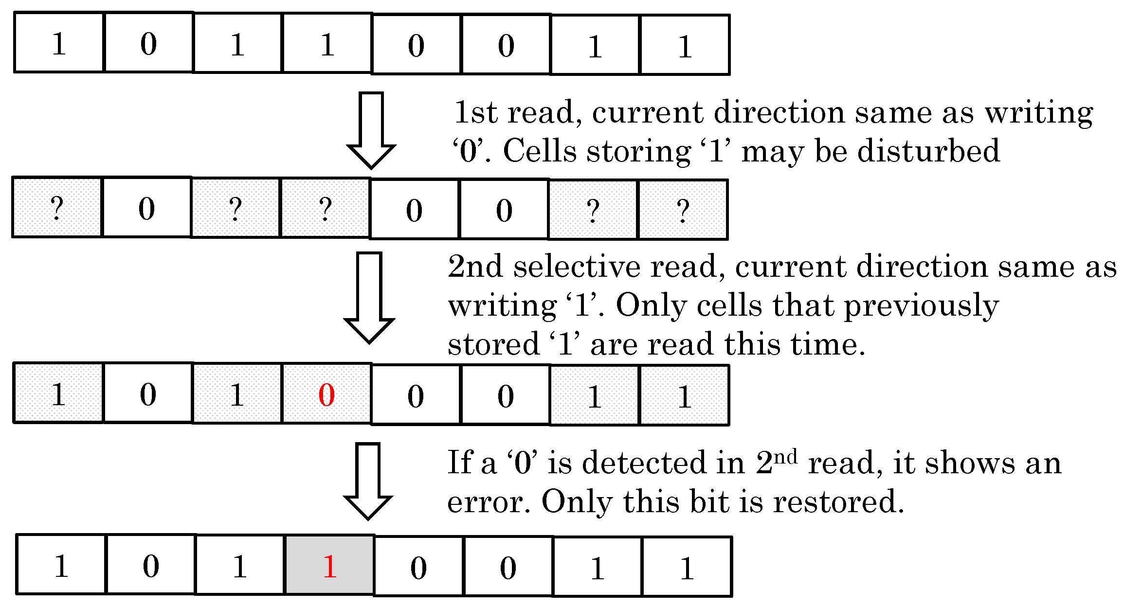
We now discuss techniques for addressing RDE in STT-RAM. Some techniques avoid restore operations by using LCLL reads [34], data compression [39], data-duplication [39], by exploiting cache/RF access properties [4,43] and by using an SRAM buffer to absorb reads for minimizing reads from STT-RAM [43]. Furthermore, restores can be scheduled at idle times to avoid their performance impact. Some techniques restore only cells with a “1” value [4,43], since only these cells may be disturbed during reads on using the current direction the same as writing “0”.

6.1. Avoiding Redundant Restore Operations

The technique of Wang et al. [4] seeks to avoid restore operations for blocks that are expected to see a write operation in the near future. In a cache hierarchy, the same data may be present in SRAM L1 cache and STT-RAM L2 cache, and hence, a read-disturbed line in L2 need not be immediately corrected. Based on this, their technique delays restore operation till the line is evicted from L1 and decides about the restore based on status of the line at the time of eviction from L1. In L1, they store a bit to show whether the line is loaded directly from main memory or from L2. Furthermore, when an L2 read is performed to load a line in L1, the dirty bit of L2 is also copied in L1, which is termed as the “P” bit. Further, each L2 line also stores a bit that is set after a read to it, indicating that the line is read-disturbed. At the time of eviction of an L1 cache line that was loaded directly from main memory, the line is evicted without restore, but if it was loaded from L2, then the line needs to be restored in L2. If the line is found in L2, it is restored in L2, but if the line is not found in L2, the evicted L1 line is directly written back to memory if its “P” bit is clear; and a restore operation is skipped if the “P” bit is set. Thus, since a read-disturbed L2 line cannot be written back to memory, their technique evicts such an L2 line and, instead, writes back the corresponding L1 line when it is evicted to maintain data integrity.
They further note that in STT-RAM, “1” and “0” bits are written by applying SL to BL current and BL to SL current, respectively, and a read operation can also use similar directions. On using the “writing-0-like” current, only cells with the “1” bit are disturbed and vice versa. Based on this, at the time of a restore operation, their technique first identifies the disturbed cells by reading the disturbed line using the inverted reading current and, then, only restores the disturbed cells. By virtue of reducing restore operations, their technique achieves a large performance improvement compared to the restore-after-read technique. This is illustrated in Figure 16.
The size of GPU RF is orders of magnitude larger than that of CPU RF and is even larger than that of the L1 and L2 caches on GPU [55,56]. Since SRAM consumes large leakage power, Zhang et al. [43] propose using STT-RAM for designing RF in GPU and present a technique to reduce the restore requirement. They characterize the RF access pattern and observe that most registers are read only once, whereas most of the remaining registers are read only two or three times. Based on this, they determine the last read to a register and avoid the restore operation after the last read operation. To reduce the restore requirement for repeatedly accessed registers, they record the number of references for every read operand of all of the instructions and store this along with the instruction. Based on this, registers with multiple reads (e.g., more than three) are stored in an SRAM buffer since SRAM does not suffer from RDE. Further, during bank conflicts, they propose restoring only 1’s regardless of whether they were disturbed. Although this consumes additional energy, it avoids the read operation before the restore operation to identify disturbed cells. In absence of conflicts, a read is performed to identify disturbed cells, and only these cells are restored to save energy. They show that their technique mitigates the performance/energy penalty of STT-RAM register restores.

6.2. Compressing Data to Reduce RDEs

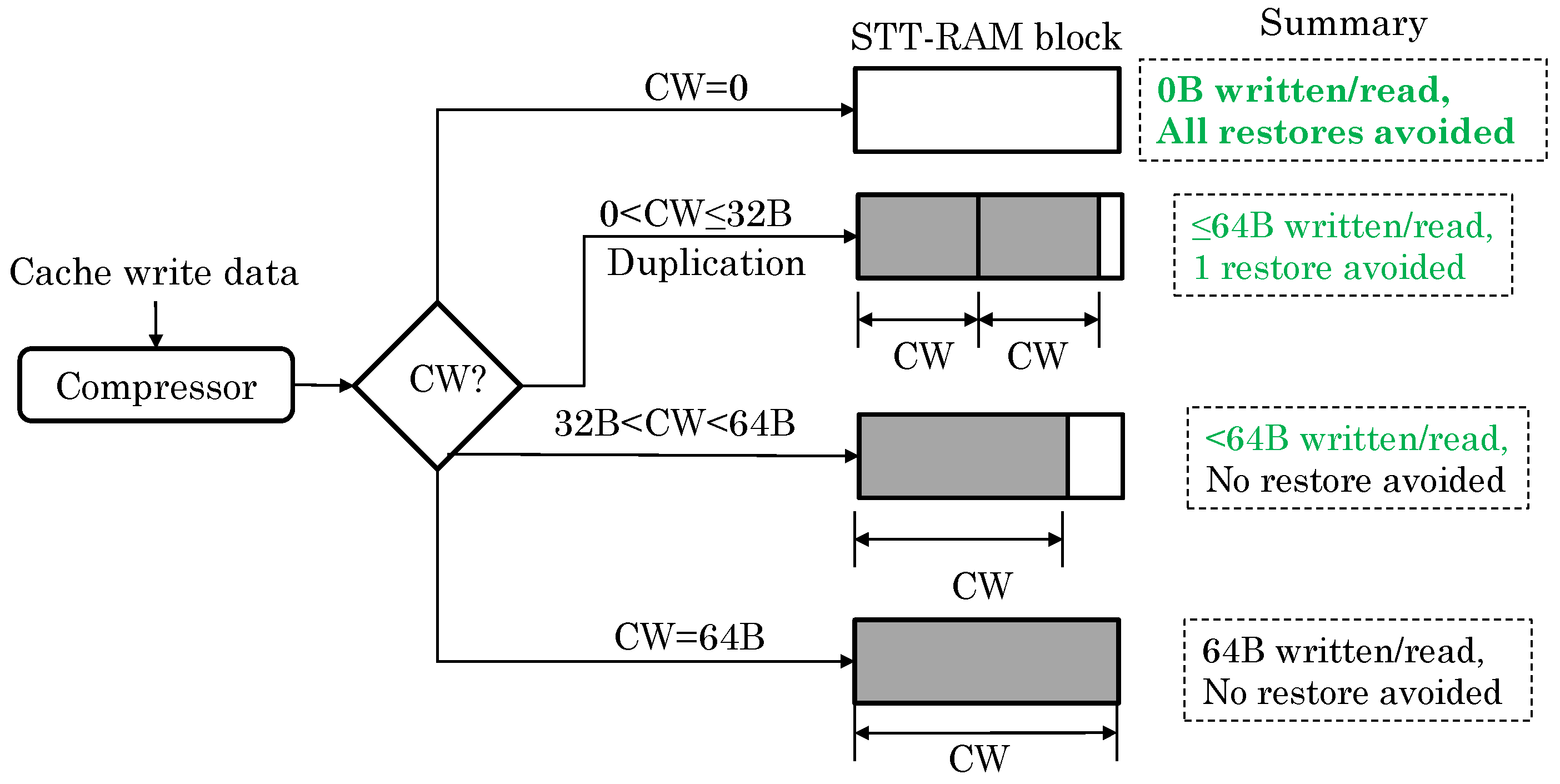
Mittal et al. [39] use data compression and selective duplication to address RDE in STT-RAM LLC. For all-zero data, their technique does not write any bits to the STT-RAM block since the data can be reconstructed from compression encoding bits on a future read operation. This avoids all restore operations for such data and also reduces read/write latency for them. For data with a compressed width ( C W ) of at most 32 B (assuming a 64-B block size), two copies are kept in the block. On the next read operation, one copy gets RDE, which is not corrected since the second copy still remains free of RDE. This avoids one restore operation for such data ( 0 < C W 32 B). Due to the reduced locality in LLC, many LLC blocks are read only once, and hence, this approach can reduce a large fraction of restore operations. For uncompressed data and those with a compressed width greater than 32 B, a single copy is kept. Figure 17 summarizes the working of their technique. On read to a block with single copy, the restore operation is performed. Compared to LCLL and restore-after-read, their technique provides higher performance and energy efficiency.

6.3. Selectively Using RDE-Free Cells or Reading Strategies

Zhang et al. [32] present a reconfigurable cache cell design for addressing RDE in STT-RAM caches. The conventional STT-RAM (called “C-mode”) requires one MTJ. They use two MTJs for storing a value and its complement and, thus, use differential sensing (i.e., compare the difference) instead of comparing against a threshold. This “D-mode” design increases the sense margin, reduces read errors and is more tolerant to process variation and the impact of process scaling. Although D-mode provides better read performance especially at smaller process nodes, its area and dynamic write power are 2× compared to C-mode. Hence, they design a reconfigurable cell that can operate as two C-mode cells or one D-mode cell. Based on this, they also propose a cache architecture where two nearby cache lines (each having its tag and valid bits) act as a “super-line”. A super-line can store two values in C-mode or one value in D-mode, and a suitable mode can be chosen at runtime based on cache level and application behavior.
They note that for L1 cache, read performance is critical, and writes account for a sizable fraction (e.g., 20%) of cache accesses. Furthermore, in an application phase, memory locations with high write traffic are rarely read, and in the later phase, the same location may be repeatedly read and infrequently written. Based on this, the L1 super-line only stores one line. Initially, writes happen in C-mode, and the neighboring line remains invalid. After a fixed number of consecutive reads to a location, the super-line switches to D-mode for future reads. A write again switches it to C-mode, and thus, intermittent reads/writes happen in C-mode, whereas consecutive reads happen in D-mode. In LLCs, frequently-accessed locations are switched to D-mode to boost read performance, and remaining lines operate in C-mode to boost capacity. Since writes contribute a much smaller fraction in LLCs, writes are allowed in D-mode also. They show that their cache design provides better performance and performance/watt compared to SRAM and STT-RAM (with all C-mode and reduced retention).
Jiang et al. [34] note that neither restore-after-read nor LCLL read provide better performance for all applications/phases. This is because when a memory bank is relatively idle, the inter-arrival time between reads is high. Hence, restore-after-read takes less time since the latency of restore operations is hidden. However, when the bank is busy, LCLL takes a smaller time to complete read operations. They propose a “smash-read” operation, which increases read current (20 μ A) to the level of write current (30 μ A) for reducing the read latency from 13 cycles to nine cycles and then uses the restore operation to address RDE. Further, they propose a “flexible-read” scheme, which issues a smash-read or LCLL read based on whether the number of entries in a bank queue is smaller than or larger than a preset threshold, respectively. This threshold is dynamically adapted for different banks depending on the distribution of accesses to them. Compared to LCLL and restore-after-read, their “flexible-read” scheme provides better main memory performance and energy efficiency.

6.4. Tolerating RDE Using the Approximate Computing Approach

The approximate computing paradigm exploits the inherent error tolerance of applications and the perceptual limitations of humans to trade precision for efficiency gains [57]. Ranjan et al. [45] present an approximate computing approach that explores the energy-quality tradeoff by allowing STT-RAM errors to save energy. They study three types of errors: (1) RDE due to reducing read duration and increasing the read current; (2) incorrect reads due to reduced read current; (3) write error due to lower write current, duration or both. They employ an additional peripheral circuitry, which allows adjusting the magnitude and duration of read/write currents to change the probability of these three errors. Based on these, they architect a configurable-quality memory array, which allows read/write operations with variable quality levels. In their technique, the error-probability for different groups of bits can be specified for controlling the magnitude of errors. They investigate the interrelationship between quality and bit-cell level energy with the help of a device-level simulator. They use this array as a scratchpad and determine the minimal quality requirement for every load/store operation for minimizing the total energy for a desired quality of result.

7. Addressing STT-RAM Write Errors

We now discuss techniques for addressing STT-RAM write errors. Some techniques divide the cache into different portions with different characteristics [6,40]. For MLC STT-RAM, some works assume a “parallel MTJs” design [30], whereas others assume a “series MTJs” design [5,6].

7.1. Partial Data Mapping

Hong et al. [30] note that in MLC STT-RAM, due to the limited difference between the resistance values of consecutive states and process variation, a state in MLC STT-RAM may be incorrectly read. To avoid this, they remove the 01 state, which has the largest overlap with adjacent states in the parallel MLC. Thus, their MLC stores only three states, which improves read stability by reducing the overlap between states and has only a small impact on density (bits stored per area) since 3LC has a smaller area than 4LC. Furthermore, it simplifies the cache controller design since the number of resistance transitions per bit-line is reduced. Data are stored in 3LC in ternary coded form, and since STT-RAM is generally used for designing LLC, the latency of ternary coding can be hidden. The MLC write operations are of three types: hard transition, which switches both hard and soft domains, soft transition, which switches only the soft domain, and two-step transition, whereby a hard and a soft transition are applied in succession. The soft transition leads to the largest write errors since in the case of insufficient switching current, no transition may take place (incomplete-write), and in the case of large current, both hard and soft domains may be switched. By removing the 01 state, the 3LC cache removes the state with the largest probability of error. Still, the 11 to 10 transition may lead to errors, and to avoid this, they use a high current, which can change both hard and soft domains. Furthermore, the soft domain is continuously monitored, and the write current is terminated as soon as the soft domain is switched to the desired state. Their 3LC cache achieves higher performance and lower energy than SLC STT-RAM LLC and higher reliability compared to MLC STT-RAM.
Wen et al. [5] present a technique to improve the read/write reliability of MLC STT-RAM. For “series MTJs” MLC, they show that the 10 state has a larger overlap with the nearby state than the 01 state. Hence, they remove the 10 state from MLC, which improves read stability and also reduces the number of erroneous transitions during MLC write operations. They use two tri-state cells to encode three binary bits. Out of nine combinations of two tri-state cells, they also remove the 0101 state, since it shows the largest error rate. Further, they use Gray coding, which ensures that up to a one-bit error (due to one erroneous transition) can occur in three-bit binary data. In their technique, changing any arbitrary state X X to 10 requires two-step transitions, viz. X X 11 01 . To reduce its performance overhead, they propose changing the state of all MLC cells to 11 before a write is scheduled to this line, which hides the latency of X X 11 transition and allows completing the write in a single programming step. They proactively change the cell state to 11 when the data in the L2 line will not be reused, which happens when: (a) a clean L1 cache line sees a write; (b) the L1 write miss is followed by a read hit to the corresponding L2 line; and (c) the L1 write miss is followed by an L2 read miss. Compared to traditional MLC STT-RAM, their technique improves read/write reliability by up to five orders of magnitude and also boosts performance. Further, compared to the SLC STT-RAM cache, their MLC STT-RAM cache achieves higher performance by virtue of higher capacity.

7.2. Using Heterogeneous Cells and/or ECCs

Wen et al. [6] show that compared to hard lines in split-cell mapping, mixed lines show lower access latency, energy and better reliability (refer to Section 2.5 for an explanation of split-cell mapping and mixed lines in MLC STT-RAM). Furthermore, hard lines show up to a five orders of magnitude higher error rate than soft lines. Based on these observations, they propose a cache composed of three lines: soft, hard and mixed. For soft and mixed lines, only low-overhead SECDED (single-error correction, double error detection) ECC is used, and mixed lines are protected at finer granularity than soft lines, since soft lines are most reliable. Since hard lines show a much higher frequency of two-bit errors than one-bit errors, they propose an ECC for hard lines, which can dynamically change between two modes. In the first mode, only one-bit errors are corrected for an overhead equal to that of SECDED. In the second mode, two-bit errors are corrected with relatively longer latency, but shorter than that of BCH codes. Although the storage requirement of their ECC is the same as that of BCH, the latency approaches that of the common case (one-bit error). They also use a data migration strategy for optimizing the use of three types of ways. For a write access directed to hard ways, a prediction is made whether it is a dead or a burst write. Dead writes are bypassed from the cache, and burst writes are swapped with the corresponding soft way. Similarly, burst writes to mixed ways are swapped with soft ways in the same set. Similarly, intensive reads to hard and mixed ways are swapped. Thus, mixed ways allow redirecting some unreliable writes from hard ways to mixed ways. They select a configuration where the cache is partitioned into hard, mixed and soft ways, such that EDP is minimized. Compared to split-cell mapping with BCH code, their cache design provides energy and performance benefits with the same level of reliability.
Wang et al. [40] present an adaptive ECC mechanism to reduce write failures in STT-RAM. A write error in STT-RAM occurs when the write pulse is terminated before the resistance of the MTJ is switched. Furthermore, the write error shows an asymmetric nature, such that the failure rate is mainly determined by the probability of 0 1 switching (and not 1 0 switching), including 0 1 flips in ECC (if used). Due to this, the requirement of ECC varies across different cache ways and over time. Based on this, they propose an adaptive ECC technique to reduce ECC overhead while providing the required ECC protection. They use a strong and a weak ECC scheme. They logically partition the ways of a cache set into two groups that use strong and weak ECC, respectively. At the time of a write, the ECC requirement of a data block is estimated based on its flips (as shown above) and a threshold. Based on this, the block is written to a suitable group.
They propose strategies to find the suitable partition of cache ways in two groups based on the ECC requirement of data blocks. Since most blocks have low flips, the weak ECC group generally has higher capacity. To account for temporal variation in ECC, the number of ways in the strong ECC group is increased compared to the average case to provide a safety margin. They also propose dynamically adapting the threshold to decide data allocation based on a change in the miss rate. While writing a block, only changed bits are updated, and hence, their technique also reduces the probability of bit-flips due to writing data with the same number of 1’s in the same group. They show that their technique provides better performance and energy efficiency, lower ECC overhead and comparable write reliability compared to the traditional ECC mechanism.

7.3. Using Error-Aware Cache Replacement Policy

Monazzah et al. [37] present a cache replacement policy for reducing write errors in STT-RAM. They note that the write error rate is directly related to the number of bit-transitions, i.e., the Hamming distance between the existing and incoming data values. L2 cache writes occur on write-backs from L1 and insertions after L2 misses. Since the Hamming distance of incoming data with different existing blocks can vary widely, the cache replacement policy that decides the location of incoming data has a significant impact on the number of bit-transitions and, hence, the error rate. While the traditional LRU (least-recently used) replacement policy replaces blocks based on their access pattern, their policy selects a replacement candidate based on the number of 0 1 transitions on writing to that block. 1 0 transitions are ignored since their error rate is two orders of magnitude lower than that of 0 1 transitions. Their policy first searches the candidate from invalid blocks and, in their absence, from valid blocks. The replacement policy is invoked on cache misses, and hence, its latency is hidden; however, it can cause extra misses by replacing useful blocks. Compared to LRU replacement policy, their technique reduces the write error rate while incurring only a small performance and energy penalty. Their technique searches the most appropriate way from all of the available ways, whereas the technique of Wang et al. [40] only searches the right group and uses the LRU policy within that group to find the appropriate way.

7.4. Using VnC and ECC Schemes

Sun et al. [42] present two schemes to address write failure in STT-RAM-based caches. First, they propose using VnC operations, where after every write, the stored value is read to ensure the correct write, and in case of errors, VnC is again issued. Since a large fraction of cache write operations bring the same data as that originally stored and STT-RAM write error happens only on a change in the stored bit, the performance penalty of VnC remains small. However, this penalty increases with a rising error rate, and for such cases, they propose using ECC with VnC, which reduces the requirement of VnC operations since VnC needs to be issued only when errors exceed the correction capability of ECC. They show that their technique can tolerate high write error rates with only a small performance, area and energy penalty.
Ahn et al. [44] present a low-overhead ECC scheme for mitigating write errors in STT-RAM L2 cache. They observe that since bit transitions on writes are relatively infrequent, a large fraction of writes is free of errors. Hence, allocating ECC for every cache block leads to resource inefficiency. They propose sharing the ECC unit between cache blocks, and thus, the number of ECC blocks can be less than the set-associativity, as shown in Figure 18. An error-free write does not use ECC. If the number of errors on a write is within the correction capability of ECC, an ECC block is allocated, whereas for a higher number of errors, the VnC scheme is used to reduce the number of bit-errors. If all ECC blocks are occupied, the data block corresponding to the oldest allocated ECC block is fully corrected using VnC, and then, the ECC block is released. Their technique reduces the requirement of VnC operations and the area overhead of ECC.

8. Conclusions and Future Outlook

In this paper, we presented a survey on techniques for improving the reliability of STT-RAM and PCM. We summarized the key architectural management ideas used by the research projects and organized them based on important parameters to underscore their differences and similarities. We conclude this paper with a brief mention of future challenges and solution directions in this area.
Given the energy inefficiency of conventional memories and the reliability issues of NVMs, it is likely that future systems will use a hybrid memory design to bring the best of NVMs and conventional memories together. For example, in an SRAM-STT-RAM hybrid cache, read-intensive blocks can be migrated to SRAM to avoid RDEs in STT-RAM, and DRAM can be used as cache to reduce write operations to PCM memory for avoiding WDEs. However, since conventional memories also have reliability issues [11], practical realization and adoption of these hybrid memory designs are expected to be as challenging as those of NVM-based memory designs. Overcoming these challenges will require concerted efforts from both academia and industry.
Existing NVM reliability solutions have mostly targeted CPU caches/memory. Given the power-constrained computing horizon and the phenomenal growth in the use of GPUs, it is likely that NVMs will be employed for designing RF, caches and memory in GPU in the very near future. However, given the fundamental differences between the architecture of CPUs and GPUs, partial retrofitting of existing NVM reliability solutions for GPUs is unlikely to be optimal or even infeasible. Hence, the design of novel GPU-specific techniques will be an interesting challenge for computer-architects.
As the applications running on systems ranging from hand-held devices to massive data centers and supercomputers become increasingly data intensive, their memory requirements are increasing at a fast rate. Since the conventional memories cannot meet the capacity demands and power budgets of these systems, NVMs appear to be the only viable solutions for these systems. Clearly, exploiting the opportunities and addressing the challenges specific to each class of system will be important to improve the efficiency of NVM reliability techniques.
Approximate computing offers a promising approach for reducing the correction overhead of NVM errors [57]. For example, approximable data, such as least significant bits of floating-point data, can be stored in NVM memory. Furthermore, ECC for such data can be skipped or the scrubbing frequency can be reduced. Clearly, relaxing the requirement of fully-correct execution opens up a variety of opportunities for managing the NVM reliability issue. However, to fully benefit from the approximate computing approach, its scope needs to be extended from multimedia applications to a wide range of general-purpose applications.

Conflicts of Interest

The author declares no conflicts of interest.

References

  1. Mittal, S.; Vetter, J.S. A Survey of Software Techniques for Using Non-Volatile Memories for Storage and Main Memory Systems. IEEE Trans. Parallel Distrib. Syst. 2016, 27, 1537–1550. [Google Scholar] [CrossRef]
  2. Seong, N.H.; Yeo, S.; Lee, H.H.S. Tri-level-cell phase change memory: Toward an efficient and reliable memory system. In Proceedings of the 40th Annual International Symposium on Computer Architecture, Tel-Aviv, Israel, 23–27 June 2013; pp. 440–451.
  3. Jiang, L.; Zhang, Y.; Yang, J. Mitigating write disturbance in super-dense phase change memories. In Proceedings of the International Conference on Dependable Systems and Networks (DSN), Atlanta, GA, USA, 23–26 June 2014; pp. 216–227.
  4. Wang, R.; Jiang, L.; Zhang, Y.; Wang, L.; Yang, J. Selective restore: an energy efficient read disturbance mitigation scheme for future STT-MRAM. In Proceedings of the 2015 52nd ACM/EDAC/IEEE Design Automation Conference, San Francisco, CA, USA, 8–12 June 2015; p. 21.
  5. Wen, W.; Zhang, Y.; Mao, M.; Chen, Y. State-restrict MLC STT-RAM designs for high-reliable high-performance memory system. In Proceedings of the 2014 51st ACM/EDAC/IEEE Design Automation Conference, San Francisco, CA, USA, –5 June 2014; pp. 1–6.
  6. Wen, W.; Mao, M.; Li, H.; Chen, Y.; Pei, Y.; Ge, N. A holistic tri-region MLC STT-RAM design with combined performance, energy, and reliability optimizations. In Proceedings of the Design, Automation & Test in Europe Conference & Exhibition (DATE), Dresden, Germany, 14–18 March 2016; pp. 1285–1290.
  7. Mittal, S.; Vetter, J. AYUSH: Extending Lifetime of SRAM-NVM Way-based Hybrid Caches Using Wear-leveling. In Proceedings of the 2015 IEEE 23rd International Symposium on Modeling, Analysis and Simulation of Computer and Telecommunication Systems (MASCOTS), Atlanta, GA, USA, 5–7 October 2015.
  8. Mittal, S.; Vetter, J.S. EqualWrites: Reducing Intra-set Write Variations for Enhancing Lifetime of Non-volatile Caches. IEEE Trans. VLSI Syst. 2016, 24, 103–114. [Google Scholar] [CrossRef]
  9. Vetter, J.S.; Mittal, S. Opportunities for Nonvolatile Memory Systems in Extreme-Scale High Performance Computing. Comput. Sci. Eng. 2015, 17, 73–82. [Google Scholar] [CrossRef]
  10. Mittal, S.; Vetter, J.S.; Li, D. A Survey Of Architectural Approaches for Managing Embedded DRAM and Non-volatile On-chip Caches. IEEE Trans. Parallel Distrib. Syst. 2015, 26, 1524–1537. [Google Scholar] [CrossRef]
  11. Mittal, S.; Vetter, J. Reliability Tradeoffs in Design of Volatile and Non-volatile Caches. J. Circuits Syst. Comput. 2016, 25, 11. [Google Scholar] [CrossRef]
  12. Mittal, S.; Vetter, J. A Survey of Techniques for Modeling and Improving Reliability of Computing Systems. IEEE Trans. Parallel Distrib. Syst. 2016, 27, 1226–1238. [Google Scholar] [CrossRef]
  13. Xu, W.; Zhang, T. A time-aware fault tolerance scheme to improve reliability of multilevel phase-change memory in the presence of significant resistance drift. IEEE Trans. Very Large Scale Integr. Syst. 2011, 19, 1357–1367. [Google Scholar] [CrossRef]
  14. Mittal, S.; Poremba, M.; Vetter, J.; Xie, Y. Exploring Design Space of 3D NVM and eDRAM Caches Using DESTINY Tool; Technical Report ORNL/TM-2014/636; Oak Ridge National Laboratory: Oak Ridge, TN, USA, 2014. [Google Scholar]
  15. Mittal, S. A Survey Of Architectural Techniques for Managing Process Variation. ACM Comput. Surv. 2016, 48, 54. [Google Scholar] [CrossRef]
  16. Awasthi, M.; Shevgoor, M.; Sudan, K.; Rajendran, B.; Balasubramonian, R.; Srinivasan, V. Efficient scrub mechanisms for error-prone emerging memories. In Proceedings of the International Symposium on High Performance Computer Architecture (HPCA), New Orleans, LA, USA, 25–29 February 2012; pp. 1–12.
  17. Zhang, W.; Li, T. Helmet: A resistance drift resilient architecture for multi-level cell phase change memory system. In Proceedings of the International Conference on Dependable Systems & Networks (DSN), Hong Kong, China, 27–30 June 2011; pp. 197–208.
  18. Jalili, M.; Arjomand, M.; Sarbazi-Azad, H. A reliable 3D MLC PCM architecture with resistance drift predictor. In Proceedings of the 2014 44th Annual IEEE/IFIP International Conference on Dependable Systems and Networks (DSN), Atlanta, GA, USA, 23–26 June 2014; pp. 204–215.
  19. Liu, C.; Yang, C. Improving multilevel PCM reliability through age-aware reading and writing strategies. In Proceedings of the International Conference on Computer Design (ICCD), Seoul, Korea, 19–22 October 2014; pp. 264–269.
  20. Yang, C.; Emre, Y.; Cao, Y.; Chakrabarti, C. Multi-tiered approach to improving the reliability of multi-level cell PRAM. In Proceedings of the IEEE Workshop on Signal Processing Systems (SiPS), Seoul, Korea, 19–22 October 2012; pp. 114–119.
  21. Yoon, D.H.; Chang, J.; Schreiber, R.S.; Jouppi, N.P. Practical nonvolatile multilevel-cell phase change memory. In Proceedings of the International Conference for High Performance Computing, Networking, Storage and Analysis (SC), Denver, CO, USA, 7–22 November 2013; pp. 1–12.
  22. Wang, R.; Jiang, L.; Zhang, Y.; Yang, J. SD-PCM: Constructing Reliable Super Dense Phase Change Memory under Write Disturbance. In Proceedings of the International Conference on Architectural Support for Programming Languages and Operating Systems, Istanbul, Turkey, 14–18 March 2015; pp. 19–31.
  23. Wang, R.; Mittal, S.; Zhang, Y.; Yang, J. Decongest: Accelerating Super-Dense PCM under Write Disturbance by Hot Page Remapping; Technical Report; IIT Hyderabad: Telangana, India, 2016. [Google Scholar]
  24. Ahn, D.H.; Song, Y.; Jeong, H.; Kim, B.; Kang, Y.S.; Ahn, D.H.; Kwon, Y.; Nam, S.W.; Jeong, G.; Kang, H.; et al. Reliability perspectives for high density PRAM manufacturing. In Proceedings of the 2011 IEEE International Electron Devices Meeting (IEDM), Washington, DC, USA, 5–7 December 2011.
  25. Mittal, S. A Survey of Power Management Techniques for Phase Change Memory. Int. J. Comput. Aided Eng. Technol. 2014, 8, 424. [Google Scholar] [CrossRef]
  26. Wang, R.; Jiang, L.; Zhang, Y.; Wang, L.; Yang, J. Exploit imbalanced cell writes to mitigate write disturbance in dense phase change memory. In Proceedings of the 2015 52nd ACM/EDAC/IEEE Design Automation Conference (DAC), San Francisco, CA, USA, 8–12 June 2015; p. 88.
  27. Kwon, K.W.; Fong, X.; Wijesinghe, P.; Panda, P.; Roy, K. High-Density and Robust STT-MRAM Array Through Device/Circuit/Architecture Interactions. IEEE Trans. Nanotechnol. 2015, 14, 1024–1034. [Google Scholar] [CrossRef]
  28. Fong, X.; Kim, Y.; Choday, S.H.; Roy, K. Failure mitigation techniques for 1T-1MTJ spin-transfer torque MRAM bit-cells. IEEE Trans. Very Large Scale Integr. Syst. 2014, 22, 384–395. [Google Scholar] [CrossRef]
  29. Zhang, Y.; Wang, X.; Chen, Y. STT-RAM cell design optimization for persistent and non-persistent error rate reduction: A statistical design view. In Proceedings of the International Conference on Computer-Aided Design, San Jose, CA, USA, 7–10 November 2011; pp. 471–477.
  30. Hong, S.; Lee, J.; Kim, S. Ternary cache: Three-valued MLC STT-RAM caches. In Proceedings of the IEEE International Conference on Computer Design (ICCD), Seoul, Korea, 19–22 October 2014; pp. 83–89.
  31. Takemura, R.; Kawahara, T.; Ono, K.; Miura, K.; Matsuoka, H.; Ohno, H. Highly-scalable disruptive reading scheme for Gb-scale SPRAM and beyond. In Proceedings of the 2010 IEEE International Memory Workshop (IMW), Seoul, Korea, 16–19 May 2010; pp. 1–2.
  32. Zhang, Y.; Li, Y.; Sun, Z.; Li, H.; Chen, Y.; Jones, A.K. Read performance: The newest barrier in scaled STT-RAM. IEEE Trans. Very Large Scale Integr. Syst. 2015, 23, 1170–1174. [Google Scholar] [CrossRef]
  33. Kang, W.; Zhao, W.; Klein, J.O.; Zhang, Y.; Chappert, C.; Ravelosona, D. High reliability sensing circuit for deep submicron spin transfer torque magnetic random access memory. Electron. Lett. 2013, 49, 1283–1285. [Google Scholar] [CrossRef]
  34. Jiang, L.; Wen, W.; Wang, D.; Duan, L. Improving Read Performance of STT-MRAM based Main Memories through Smash Read and Flexible Read. In Proceedings of the 2016 21st Asia and South Pacific Design Automation Conference (ASP-DAC), Macao, China, 25–28 January 2016.
  35. Mittal, S. A Survey Of Cache Bypassing Techniques. MDPI J. Low Power Electron. Appl. 2016, 6, 5. [Google Scholar] [CrossRef]
  36. Oboril, F.; Bishnoi, R.; Ebrahimi, M.; Tahoori, M. Evaluation of Hybrid Memory Technologies using SOT-MRAM for On-Chip Cache Hierarchy. IEEE Trans. Comput.-Aided Des. Integr. Circuits Syst. 2015, 34, 367–380. [Google Scholar] [CrossRef]
  37. Monazzah, A.; Farbeh, H.; Miremadi, S. LER: Least Error Rate Replacement Algorithm for Emerging STT-RAM Caches. IEEE Trans. Device and Mater. Reliab. 2016, 16, 220–226. [Google Scholar] [CrossRef]
  38. Mittal, S. A Survey of Architectural Techniques For Improving Cache Power Efficiency. Sustain. Comput. Inform. Syst. 2014, 4, 33–43. [Google Scholar] [CrossRef]
  39. Mittal, S.; Vetter, J.; Jiang, L. Addressing Read-disturbance Issue in STT-RAM by Data Compression and Selective Duplication. IEEE Comput. Archit. Lett. 2016. [Google Scholar] [CrossRef]
  40. Wang, X.; Mao, M.; Eken, E.; Wen, W.; Li, H.; Chen, Y. Sliding Basket: An adaptive ECC scheme for runtime write failure suppression of STT-RAM cache. In Proceedings of the Design, Automation & Test in Europe Conference & Exhibition (DATE), Dresden, Germany, 14–18 March 2016; pp. 762–767.
  41. Wen, W.; Mao, M.; Zhu, X.; Kang, S.H.; Wang, D.; Chen, Y. CD-ECC: Content-dependent error correction codes for combating asymmetric nonvolatile memory operation errors. In Proceedings of the International Conference on Computer-Aided Design, San Jose, CA, USA, 18–21 November 2013; pp. 1–8.
  42. Sun, H.; Liu, C.; Zheng, N.; Min, T.; Zhang, T. Design techniques to improve the device write margin for MRAM-based cache memory. In Proceedings of the 21st edition of the great lakes symposium on Great lakes symposium on VLSI, Lausanne, Switzerland, 2–4 May 2011; pp. 97–102.
  43. Zhang, H.; Chen, X.; Xiao, N.; Liu, F.; Chen, Z. Red-Shield: Shielding Read Disturbance for STT-RAM Based Register Files on GPUs. In Proceedings of the 2016 International Great Lakes Symposium on VLSI (GLSVLSI), Boston, MA, USA, 18–20 May 2016; pp. 389–392.
  44. Ahn, J.; Yoo, S.; Choi, K. Selectively protecting error-correcting code for area-efficient and reliable STT-RAM caches. In Proceedings of the 2013 18th Asia and South Pacific Design Automation Conference (ASP-DAC), Yokohama, Japan, 22–25 January 2013; pp. 285–290.
  45. Ranjan, A.; Venkataramani, S.; Fong, X.; Roy, K.; Raghunathan, A. Approximate storage for energy efficient spintronic memories. In Proceedings of the Design Automation Conference, San Francisco, CA, USA, 7–11 June 2015; p. 195.
  46. Li, B.; Pei, Y.; Wen, W. Efficient Low-Density Parity-Check (LDPC) Code Decoding for Combating Asymmetric Errors in STT-RAM. In Proceedings of the 2016 IEEE Computer Society Annual Symposium on VLSI (ISVLSI), Pittsburgh, PA, USA, 11–13 July 2016.
  47. Wang, R.; Zhang, Y.; Yang, J. ReadDuo: Constructing Reliable MLC Phase Change Memory through Fast and Robust Readout. In Proceedings of the 2016 46th Annual IEEE/IFIP International Conference on Dependable Systems and Networks (DSN), Toulouse, France, 28 June–1 July 2016.
  48. Eslami, A.; Velasco, A.; Vahid, A.; Mappouras, G.; Calderbank, R.; Sorin, D.J. Writing without Disturb on Phase Change Memories by Integrating Coding and Layout Design. In Proceedings of the International Symposium on Memory Systems, Washington, DC, USA, 5–8 October 2015; pp. 71–77.
  49. Jalili, M.; Sarbazi-Azad, H. A compression-based morphable PCM architecture for improving resistance drift tolerance. In Proceedings of the International Conference on Application-specific Systems, Architectures and Processors (ASAP), Zurich, Switzerland, 18–22 June 2014; pp. 232–239.
  50. Asadinia, M.; Arjomand, M.; Sarbazi-Azad, H. Variable resistance spectrum assignment in phase change memory systems. IEEE Trans. VLSI 2015, 23, 2657–2670. [Google Scholar] [CrossRef]
  51. Swami, S.; Mohanram, K. E3R: Energy Efficient Error Recovery for Multi/Triple-Level Cell Non-volatile Memories. In Proceedings of the 2016 19th International Conference on VLSI Design and 2016 15th International Conference on Embedded Systems (VLSID), Kolkata, India, 4–8 January 2016; pp. 373–378.
  52. Yoon, D.H.; Muralimanohar, N.; Chang, J.; Ranganathan, P.; Jouppi, N.P.; Erez, M. FREE-p: Protecting non-volatile memory against both hard and soft errors. In Proceedings of the International Symposium on High Performance Computer Architecture (HPCA), San Antonio, TX, USA, 12–16 Feburary 2011; pp. 466–477.
  53. Mittal, S.; Vetter, J. A Survey Of Architectural Approaches for Data Compression in Cache and Main Memory Systems. IEEE Trans. Parallel and Distrib. Syst. 2016, 27, 1524–1536. [Google Scholar] [CrossRef]
  54. Schechter, S.; Loh, G.H.; Straus, K.; Burger, D. Use ECP, Not ECC, for Hard Failures in Resistive Memories. In Proceedings of the International Symposium on Computer Architecture (ISCA), Saint-Malo, France, 19–23 June 2010; pp. 141–152.
  55. NVIDIA. NVIDIA’s Next Generation CUDA Compute Architecture: Kepler GK110/210. 2014. Available online: http://goo.gl/qOSWW1 (accessed on 9 February 2016).
  56. Mittal, S. A Survey of Techniques for Architecting and Managing GPU Register File. IEEE Trans. Parallel Distrib. Syst. 2017, 28, 16–28. [Google Scholar] [CrossRef]
  57. Mittal, S. A Survey Of Techniques for Approximate Computing. ACM Comput. Surv. 2016, 48, 62. [Google Scholar] [CrossRef]
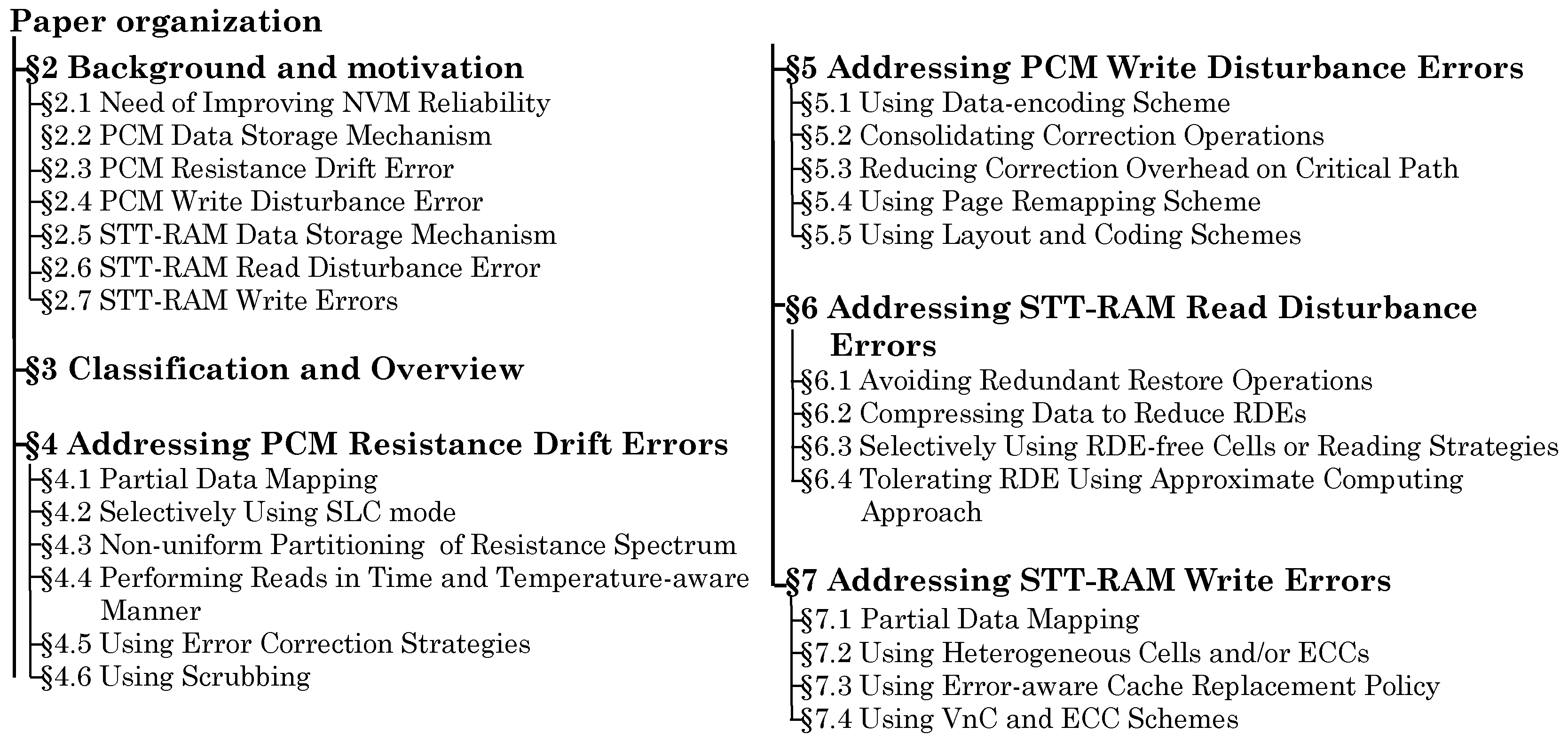
Figure 1. Overall organization of the paper.
Computers 06 00008 g001
Figure 2. Illustration of the resistance drift phenomenon in multi-level cell (MLC) PCM with static sensing ( Φ 1 , Φ 2 and Φ 3 are boundary resistance thresholds). Two solution schemes: time-aware sensing [13,18,19,20] and tri-level cell [2,21].
Computers 06 00008 g002
Figure 3. Illustration of write disturbance error.
Computers 06 00008 g003
Figure 4. (a) SLC STT-RAM; (b) parallel and (c) serial MLC STT-RAM designs.
Computers 06 00008 g004
Figure 5. (a) Direct, (b) interleaved and (c) split-cell strategies for mapping data to MLC memory.
Computers 06 00008 g005
Figure 6. Scaling of the read/write current in STT-RAM [31].
Computers 06 00008 g006
Figure 7. (a) Read and (b) write operation in MLC STT-RAM.
Computers 06 00008 g007
Figure 8. Converting original data to drift-tolerant data using (a) bit-rotation, (b) bit-inversion and (c) a combination of both [17].
Computers 06 00008 g008
Figure 9. Compression-based technique for addressing PCM resistance drift [49].
Computers 06 00008 g009
Figure 10. Example of chained remapping (solid line) and limiting the number of redirections by directly storing the final address (dashed line) [52].
Computers 06 00008 g010
Figure 11. Flow diagram of the technique of Jiang et al. [3].
Computers 06 00008 g011
Figure 12. Illustration of ( p , q ) encoding, (a) (2,3) encoding, (b) (3,4) encoding [3].
Computers 06 00008 g012
Figure 13. Illustration of 2Xdivision write on an eight-cell group [26].
Computers 06 00008 g013
Figure 14. Page remapping-based write disturbance error (WDE) mitigation technique, (a before remapping, (b) after remapping [23].
Computers 06 00008 g014
Figure 15. Checkerboard configuration of the PCM array to address WDE [48].
Computers 06 00008 g015
Figure 16. Data-aware selective restore operation [4].
Computers 06 00008 g016
Figure 17. Data compression and selective duplication-based technique for addressing read disturbance error (RDE) [39].
Computers 06 00008 g017
Figure 18. (a) Conventional ECC scheme and (b) selective-ECC scheme ( N > M ) [44].
Computers 06 00008 g018
Table 1. An overview of reliability issues discussed in this paper († since SLC PCM uses wide resistance margins, drift does not lead to errors in it [16]). SLC, single-level cell; MLC, multi-level cell.
MemorySLCMLCWhereWhenComments
Resistance driftPCMNo†YesSame cellOver timeChange in resistance changes the bit stored
Write disturbancePCMYesYesNearby cellsDuring writeWrite to a cell changes neighboring cells
Read disturbanceSTT-RAMYesYesSame cellDuring readRead changes the stored value
Write failureSTT-RAMYesYesSame cellDuring writeWritten value is incorrect
Table 2. A classification based on memory technology, cell-type and reliability issues addressed.
ClassificationReferences
Memory technology
STT-RAM[4,6,27,30,32,34,36,37,39,40,41,42,43,44,45,46]
PCM[2,3,13,16,17,18,19,20,21,22,23,26,47,48,49,50,51,52]
MLC or SLC
MLC[2,3,5,6,13,16,17,18,19,20,21,30,47,49,50,51]
SLCNearly all others
Vulnerability addressed
Resistance drift[2,13,16,17,18,20,21,47,49,50,52]
Write-disturbance[3,22,23,26,48]
Read-disturbance[4,32,34,36,39,43,45]
STT-RAM write error[5,6,30,37,40,41,42,44,45,46]
Table 3. A classification based on the processing unit, component, optimization objective and management approach. VnC, verify and correct.
ClassificationReferences
Processing unit
GPU[43]
Vector processor[45]
CPUNearly all others
Processor component where NVM is used
Main memory[2,3,16,18,21,22,23,26,34,47,49,50,51,52]
Last level Cache[4,30,32,36,39,41,42,44]
First level cache[32,36]
Register file[43]
Scratchpad[45]
Optimization objective
ReliabilityNearly all
Performance[2,4,5,6,22,23,30,32,34,36,37,39,40,41,42,43,44,47,49,50,51,52]
Energy[4,6,16,17,18,23,30,32,34,36,37,39,40,42,43,45,47,49,50,51]
Architectural management approach
ECC[3,5,6,16,27,40,41,42,44,47,49,52]
Data-duplication[39,49]
Partial data mapping[2,3,5,21,30,51]
Leveraging asymmetry of 0 1 and 1 0 transitions[37,40,41]
Gray coding[5,18,20,21]
Bit-inversion[3,17,20,27]
Bit-rotation[17]
Compression[3,26,39,49]
Use of buffer[5,43]
VnC scheme[3,22,37,42,44]
Scrubbing scheme[16,21,47]
Table 4. Illustration of 3-on-2 coding [21].
First Cell StateSecond Cell State3-Bit Data
S0S0000
S0S1001
S0S3010
S1S0011
S1S1100
S1S3101
S3S0110
S3S1111
S3S3invalid