Demonstration of a Robust All-Silicon-Carbide Intracortical Neural Interface

 , and
, and 
Abstract
1. Introduction
2. Materials and Methods
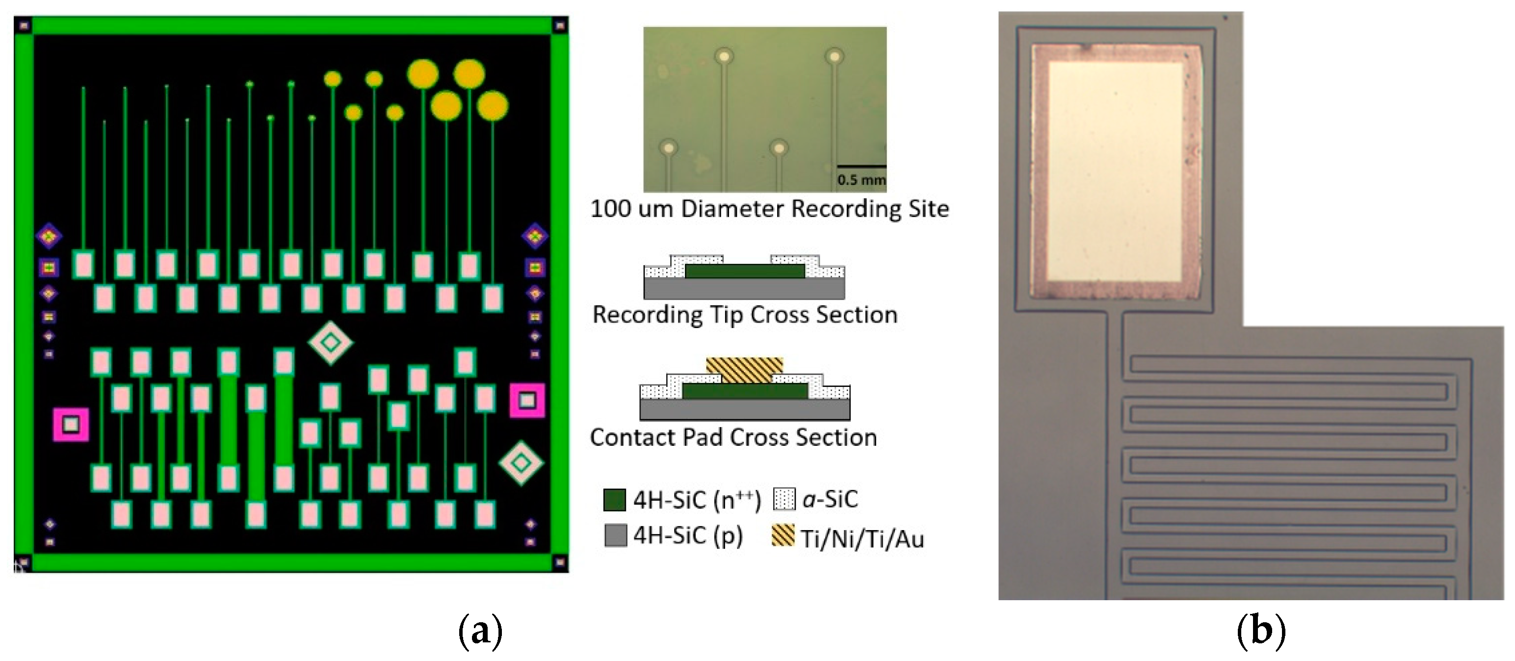
2.1. All-SiC Device Fabrication Process
2.2. All-SiC Evaluation Devices
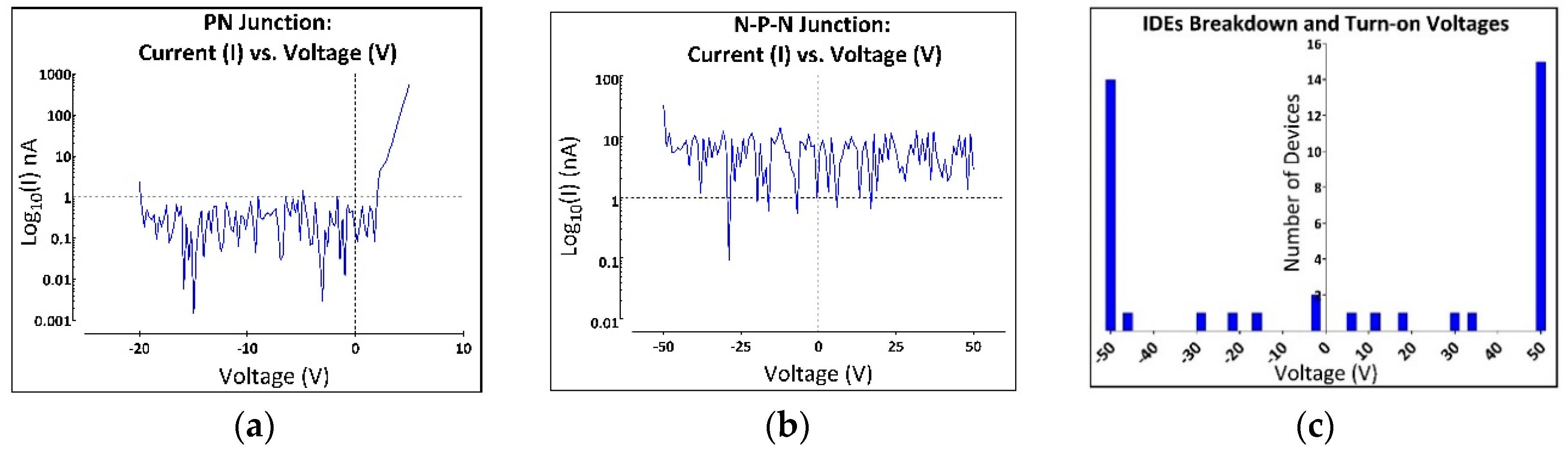
2.3. SiC Doping and PN Isolation Evaluation
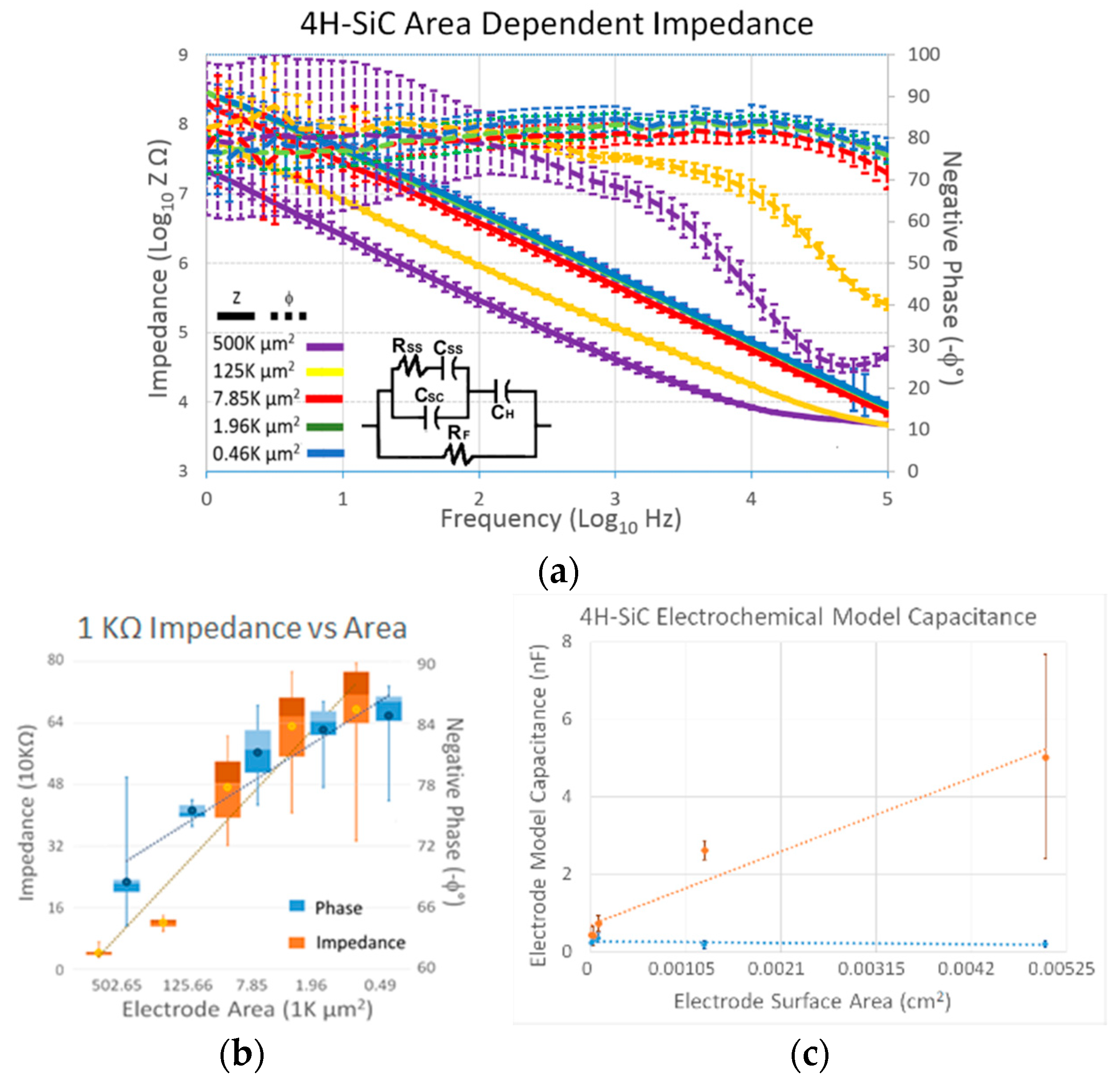
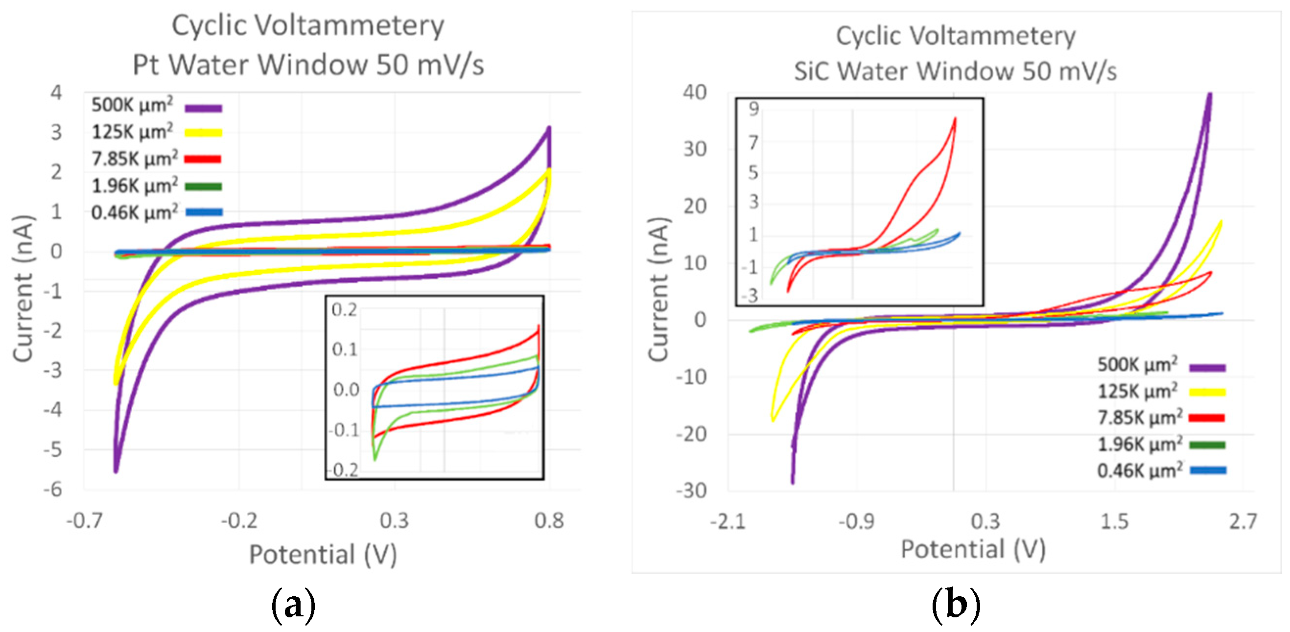
2.4. Electrochemical Characterization of 4H-SiC Material
3. Results
3.1. Device Characterization
3.2. Electrochemical Characterization
4. Discussion
5. Conclusions
Author Contributions
Funding
Acknowledgments
Conflicts of Interest
References
- Donoghue, J.P. Bridging the brain to the world: A perspective on neural interface systems. Neuron 2008, 60, 511–521. [Google Scholar] [CrossRef] [PubMed]
- Lebedev, M.A.; Nicolelis, M.A.L. Brain-machine interfaces: Past, present and future. Trends Neurosci. 2006, 29, 536–546. [Google Scholar] [CrossRef] [PubMed]
- Wolpaw, J.R.; Birbaumer, N.; McFarland, D.J.; Pfurtscheller, G.; Vaughan, T.M. Brain-computer interfaces for communication and control. Clin. Neurophysiol. 2002, 113, 767–791. [Google Scholar] [CrossRef]
- Lobel, D.A.; Lee, K.H. Brain machine interface and limb reanimation technologies: Restoring function after spinal cord injury through development of a bypass system. Mayo Clin. Proc. 2014, 89, 708–714. [Google Scholar] [CrossRef] [PubMed]
- Maynard, E.M.; Nordhausen, C.T.; Normann, R.A. The Utah intracortical electrode array: A recording structure for potential brain-computer interfaces. Electroencephalogr. Clin. Neurophysiol. 1997, 102, 228–239. [Google Scholar] [CrossRef]
- Jorfi, M.; Skousen, J.L.; Weder, C.; Capadona, J.R. Progress towards biocompatible intracortical microelectrodes for neural interfacing applications. J. Neural Eng. 2015, 12, 011001. [Google Scholar] [CrossRef] [PubMed]
- Luo, Y.H.-L.; da Cruz, L. The argus® II retinal prosthesis system. Prog. Retin. Eye Res. 2016, 50, 89–107. [Google Scholar] [CrossRef] [PubMed]
- Markowitz, M.; Rankin, M.; Mongy, M.; Patino, B.E.; Manusow, J.; Devenyi, R.G.; Markowitz, S.N. Rehabilitation of lost functional vision with the argus ii retinal prosthesis. Can. J. Ophthalmol. 2018, 53, 14–22. [Google Scholar] [CrossRef] [PubMed]
- Clark, G.M. The multi-channel cochlear implant: Multi-disciplinary development of electrical stimulation of the cochlea and the resulting clinical benefit. Hear. Res. 2015, 322, 4–13. [Google Scholar] [CrossRef] [PubMed]
- Aziliz, L.; Emeline, D.; Christian, B. A review on mechanical considerations for chronically-implanted neural probes. J. Neural Eng. 2018, 15, 031001. [Google Scholar]
- Rousche, P.J.; Normann, R.A. Chronic recording capability of the utah intracortical electrode array in cat sensory cortex. J. Neurosci. Methods 1998, 82, 1–15. [Google Scholar] [CrossRef]
- Barrese, J.C.; Aceros, J.; Donoghue, J.P. Scanning electron microscopy of chronically implanted intracortical microelectrode arrays in non-human primates. J. Neural Eng. 2016, 13, 026003. [Google Scholar] [CrossRef] [PubMed]
- Barrese, J.C.; Rao, N.; Paroo, K.; Triebwasser, C.; Vargas-Irwin, C.; Franquemont, L.; Donoghue, J.P. Failure mode analysis of silicon-based intracortical microelectrode arrays in non-human primates. J. Neural Eng. 2013, 10, 066014. [Google Scholar] [CrossRef] [PubMed]
- Griffith, R.W.; Humphrey, D.R. Long-term gliosis around chronically implanted platinum electrodes in the rhesus macaque motor cortex. Neurosci. Lett. 2006, 406, 81–86. [Google Scholar] [CrossRef] [PubMed]
- Kotov, N.A.; Winter, J.O.; Clements, I.P.; Jan, E.; Timko, B.P.; Campidelli, S.; Pathak, S.; Mazzatenta, A.; Lieber, C.M.; Prato, M.; et al. Nanomaterials for neural interfaces. Adv. Mater. 2009, 21, 3970–4004. [Google Scholar] [CrossRef]
- Prasad, A.; Xue, Q.S.; Sankar, V.; Nishida, T.; Shaw, G.; Streit, W.J.; Sanchez, J.C. Comprehensive characterization and failure modes of tungsten microwire arrays in chronic neural implants. J. Neural Eng. 2012, 9, 056015. [Google Scholar] [CrossRef] [PubMed]
- Massey, L.K. Permeability Properties of Plastics and Elastomers: A Guide to Packaging and Barrier Materials, 2nd ed.; William Andrew: Norwich, NY, USA, 2002. [Google Scholar]
- Jones, D. Principles and Prevention of Corrosion, 2nd ed.; Prentice-Hall: Upper Saddle River, NJ, USA, 1996. [Google Scholar]
- Deiasi, R.; Russell, J. Aqueous degradation of polyimides. J. Appl. Polym. Sci. 1971, 15, 2965–2974. [Google Scholar] [CrossRef]
- Rubehn, B.; Stieglitz, T. In vitro evaluation of the long-term stability of polyimide as a material for neural implants. Biomaterials 2010, 31, 3449–3458. [Google Scholar] [CrossRef] [PubMed]
- Polikov, V.S.; Tresco, P.A.; Reichert, W.M. Response of brain tissue to chronically implanted neural electrodes. J. Neurosci. Methods 2005, 148, 1–18. [Google Scholar] [CrossRef] [PubMed]
- Nordhausen, C.T.; Maynard, E.M.; Normann, R.A. Single unit recording capabilities of a 100 microelectrode array. Brain Res. 1996, 726, 129–140. [Google Scholar] [CrossRef]
- Kipke, D.R.; Vetter, R.J.; Williams, J.C.; Hetke, J.F. Silicon-substrate intracortical microelectrode arrays for long-term recording of neuronal spike activity in cerebral cortex. IEEE Trans. Neural Syst. Rehabil. Eng. 2003, 11, 151–155. [Google Scholar] [CrossRef] [PubMed]
- Cogan, S.F. Neural stimulation and recording electrodes. Annu. Rev. Biomed. Eng. 2008, 10, 275–309. [Google Scholar] [CrossRef] [PubMed]
- Saddow, S.E.; Frewin, C.L.; Nezafati, M.; Oliveros, A.; Afroz, S.; Register, J.; Reyes, M.; Thomas, S. 3C-SiC on Si: A bio- and hemo-compatible material for advanced nano-bio devices. In Proceedings of the 2014 IEEE 9th Nanotechnology Materials and Devices Conference (NMDC), Aci Castello, Italy, 12–15 October 2014; pp. 49–53. [Google Scholar]
- Frewin, C.L.; Locke, C.; Saddow, S.E.; Weeber, E.J. Biocompatibility of sic for neurological applications. In Silicon Carbide Biotechnology: A Biocompatible Semiconductor for Advanced Biomedical Devices and Applications, 1st ed.; Saddow, S.E., Ed.; Elsevier: Oxford, UK, 2011. [Google Scholar]
- Frewin, L.C.; Coletti, C.; Register, J.J.; Nezafati, M.; Thomas, S.; Saddow, E.S. Silicon carbide materials for biomedical applications. In Carbon for Sensing Devices; Demarchi, D., Tagliaferro, A., Eds.; Springer: Cham, Switzerland, 2015; pp. 153–207. [Google Scholar]
- Lei, X.; Kane, S.; Cogan, S.; Lorach, H.; Galambos, L.; Huie, P.; Mathieson, K.; Kamins, T.; Harris, J.; Palanker, D. Sic protective coating for photovoltaic retinal prosthesis. J. Neural Eng. 2016, 13, 046016. [Google Scholar] [CrossRef] [PubMed]
- Saddow, S.E.; Frewin, C.; Reyes, M.; Register, J.; Nezafati, M.; Thomas, S. 3C-SiC on Si: A biocompatible material for advanced bioelectronic devices. ECS Trans. 2014, 61, 101–111. [Google Scholar] [CrossRef]
- Zorman, C.A. Silicon carbide as a material for biomedical microsystems. In Proceedings of the 2009 Symposium on Design, Test, Integration & Packaging of MEMS/MOEMS, Rome, Italy, 1–3 April 2009; pp. 1–7. [Google Scholar]
- Frewin, C.L.; Locke, C.; Mariusso, L.; Weeber, E.J.; Saddow, S.E. Silicon carbide neural implants: In vivo neural tissue reaction. In Proceedings of the 2013 6th International IEEE/EMBS Conference on Neural Engineering (NER), San Diego, CA, USA, 6–8 November 2013; pp. 661–664. [Google Scholar]
- Cogan, S.F.; Edell, D.J.; Guzelian, A.A.; Ping Liu, Y.; Edell, R. Plasma-enhanced chemical vapor deposited silicon carbide as an implantable dielectric coating. J. Biomed. Mater. Res. A 2003, 67, 856–867. [Google Scholar] [CrossRef] [PubMed]
- Deku, F.; Cohen, Y.; Joshi-Imre, A.; Kanneganti, A.; Gardner, T.J.; Cogan, S.F. Amorphous silicon carbide ultramicroelectrode arrays for neural stimulation and recording. J. Neural Eng. 2018, 15, 016007. [Google Scholar] [CrossRef] [PubMed]
- Henry, A.; ul Hassan, J.; Bergman, J.P.; Hallin, C.; Janzén, E. Thick silicon carbide homoepitaxial layers grown by cvd techniques. Chem. Vapor Depos. 2006, 12, 475–482. [Google Scholar] [CrossRef]
- Hassan, J.; Bae, H.T.; Lilja, L.; Farkas, I.; Kim, I.; Stenberg, P.; Sun, J.W.; Kordina, O.; Bergman, P.; Ha, S.Y.; Janzén, E. Fast growth rate epitaxy on 4° off-cut 4-inch diameter 4H-SiC wafers. Mater. Sci. Forum 2014, 778–780, 179–182. [Google Scholar] [CrossRef]
- Saxena, V.; Steckl, A.J. Chapter 3 building blocks for sic devices: Ohmic contacts, schottky contacts, and p-n junctions. In Semiconductors and Semimetals; Soo Park, Y., Ed.; Elsevier: New York, NY, USA, 1998; Volume 52, pp. 77–160. [Google Scholar]
- Feng, X.; Huang, Y.; Rosakis, A.J. On the stoney formula for a thin film/substrate system with nonuniform substrate thickness. J. Appl. Mech. 2007, 74, 1276–1281. [Google Scholar] [CrossRef]
- Bernardin, E.; Frewin, C.L.; Dey, A.; Everly, R.; ul Hassan, J.; Janzén, E.; Pancrazio, J.; Saddow, S.E. Development of an all-sic neuronal interface device. MRS Adv. 2016, 1, 3679–3684. [Google Scholar] [CrossRef]
- Schroder, D.K. Semiconductor material and device characterization. In Carrier and Doping Density, 3rd ed.; John Wiley and Sons, Inc.: Hoboken, NJ, USA, 2006; p. 779. [Google Scholar]
- Allongue, P.; Cachet, H. Band-edge shift and surface-charges at illuminated n-GaAs aqueous electrolyte junctions. Surface state analysis and simulation of their occupation rate. J. Electrochem. Soc. 1985, 132, 45–52. [Google Scholar] [CrossRef]
- Peter, L.M. Semiconductor electrochemistry. In Photoelectrochemical Solar Fuel Production; Giménez, S., Bisquert, J., Eds.; Springer: Cham, Switzerland, 2016. [Google Scholar]
- Rose, T.L.; Robblee, L.S. Electrical-stimulation with pt electrodes. VIII. Electrochemically safe charge injection limits with 0.2 ms pulses. IEEE Trans. Biomed. Eng. 1990, 37, 1118–1120. [Google Scholar] [CrossRef] [PubMed]
- Peters, D.; Schorner, R.; Holzlein, K.-H.; Friedrichs, P. Planar aluminum-implanted 1400 V 4h silicon carbide p-n diodes with low on resistance. Appl. Phys. Lett. 1997, 71, 2996–2997. [Google Scholar] [CrossRef]
- Mitlehner, H.; Friedrichs, P.; Peters, D.; Schorner, R.; Weinert, U.; Weis, B.; Stephani, D. Switching behaviour of fast high voltage sic pn-diodes. In Proceedings of the 10th International Symposium on Power Semiconductor Devices and ICs (ISPSD’98), Kyoto, Japan, 3–6 June 1998; pp. 127–130. [Google Scholar]
- McConnell, G.C.; Rees, H.D.; Levey, A.I.; Gutekunst, C.A.; Gross, R.E.; Bellamkonda, R.V. Implanted neural electrodes cause chronic, local inflammation that is correlated with local neurodegeneration. J. Neural Eng. 2009, 6, 056003. [Google Scholar] [CrossRef] [PubMed]
- Prasad, A.; Xue, Q.-S.; Dieme, R.; Sankar, V.; Mayrand, R.; Nishida, T.; Streit, W.; Sanchez, J. Abiotic-biotic characterization of pt/ir microelectrode arrays in chronic implants. Front. Neuroeng. 2014, 7. [Google Scholar] [CrossRef] [PubMed]
- Simon, D.M.; Charkhkar, H.; St. John, C.; Rajendran, S.; Kang, T.; Reit, R.; Arreaga-Salas, D.; McHail, D.G.; Knaack, G.L.; Sloan, A.; et al. Design and demonstration of an intracortical probe technology with tunable modulus. J. Biomed. Mater. Res. A 2017, 105, 159–168. [Google Scholar] [CrossRef] [PubMed]
- Reit, R.; Zamorano, D.; Parker, S.; Simon, D.; Lund, B.; Voit, W.; Ware, T.H. Hydrolytically stable thiol-ene networks for flexible bioelectronics. ACS Appl. Mater. Interfaces 2015, 7, 28673–28681. [Google Scholar] [CrossRef] [PubMed]
- Teo, A.J.T.; Mishra, A.; Park, I.; Kim, Y.-J.; Park, W.-T.; Yoon, Y.-J. Polymeric biomaterials for medical implants and devices. ACS Biomater. Sci. Eng. 2016, 2, 454–472. [Google Scholar] [CrossRef]
- Kozai, T.D.Y.; Catt, K.; Li, X.; Gugel, Z.V.; Olafsson, V.T.; Vazquez, A.L.; Cui, X.T. Mechanical failure modes of chronically implanted planar silicon-based neural probes for laminar recording. Biomaterials 2015, 37, 25–39. [Google Scholar] [CrossRef] [PubMed]
- Kip, A.L.; Jeffrey, D.U.; Junyan, Y.; David, C.M.; Daryl, R.K. Chronic neural recordings using silicon microelectrode arrays electrochemically deposited with a poly(3,4-ethylenedioxythiophene) (pedot) film. J. Neural Eng. 2006, 3, 59–70. [Google Scholar]
- Wilks, S.; Richardson-Burn, S.; Hendricks, J.; Martin, D.; Otto, K. Poly(3,4-ethylene dioxythiophene) (pedot) as a micro-neural interface material for electrostimulation. Front. Neuroeng. 2009, 2, 7. [Google Scholar] [CrossRef] [PubMed]
- Aqrawe, Z.; Montgomery, J.; Travas-Sejdic, J.; Svirskis, D. Conducting polymers for neuronal microelectrode array recording and stimulation. Sens. Actuat. B Chem. 2018, 257, 753–765. [Google Scholar] [CrossRef]
- Block, M.L.; Hong, J.S. Microglia and inflammation-mediated neurodegeneration: Multiple triggers with a common mechanism. Prog. Neurobiol. 2005, 76, 77–98. [Google Scholar] [CrossRef] [PubMed]
- McHardy, J.; Geller, D.; Brummer, S.B. An approach to corrosion control during electrical stimulation. Ann. Biomed. Eng. 1977, 5, 144–149. [Google Scholar] [CrossRef] [PubMed]
- Cogan, S.F.; Ludwig, K.A.; Welle, C.G.; Takmakov, P. Tissue damage thresholds during therapeutic electrical stimulation. J. Neural Eng. 2016, 13, 021001. [Google Scholar] [CrossRef] [PubMed]
- Do, D.-H.; Ecker, M.; Voit, W.E. Characterization of a thiol-ene/acrylate-based polymer for neuroprosthetic implants. ACS Omega 2017, 2, 4604–4611. [Google Scholar] [CrossRef] [PubMed]
- Jones, K.E.; Campbell, P.K.; Normann, R.A. Interelectrode isolation in a penetrating intracortical electrode array. In Proceedings of the Twelfth Annual International Conference of the IEEE Engineering in Medicine and Biology Society, Philadelphia, PA, USA, 1–4 November 1990; pp. 496–497. [Google Scholar]
- Jones, K.E.; Campbell, P.K.; Normann, R.A. A glass/silicon composite intracortical electrode array. Ann. Biomed. Eng. 1992, 20, 423–437. [Google Scholar] [CrossRef] [PubMed]
- Branner, A.; Stein, R.B.; Fernandez, E.; Aoyagi, Y.; Normann, R.A. Long-term stimulation and recording with a penetrating microelectrode array in cat sciatic nerve. IEEE Trans. Biomed. Eng. 2004, 51, 146–157. [Google Scholar] [CrossRef] [PubMed]
- Tanaka, A. Toxicity of indium arsenide, gallium arsenide, and aluminium gallium arsenide. Toxicol. Appl. Pharmacol. 2004, 198, 405–411. [Google Scholar] [CrossRef] [PubMed]
- Pakes, A.; Skeldon, P.; Thompson, G.E.; Fraser, J.W.; Moisa, S.; Sproule, G.I.; Graham, M.J.; Newcomb, S.B. Anodic oxidation of gallium nitride. J. Mater. Sci. 2003, 38, 343–349. [Google Scholar] [CrossRef]
- Kashiwada, T.; Watanabe, T.; Ootani, Y.; Tateyama, Y.; Einaga, Y. A study on electrolytic corrosion of boron-doped diamond electrodes when decomposing organic compounds. ACS Appl. Mater. Interfaces 2016, 8, 28299–28305. [Google Scholar] [CrossRef] [PubMed]
- Pan, M.; Liang, L.; Lin, W.; Kim, S.M.; Li, Q.; Kong, J.; Dresselhaus, M.S.; Meunier, V. Modification of the electronic properties of hexagonal boron-nitride in bn/graphene vertical heterostructures. 2D Mater. 2016, 3, 045002. [Google Scholar] [CrossRef]
- Saddow, S.E. SiC biotechnology for advanced biomedical applications. In Second Workshop on Advanced Cybernetics; University of Sao Paulo: Sao Carlos, Brasil, 2013. [Google Scholar]
- Saddow, S.E. Silicon Carbide Biotechnology: A Biocompatible Semiconductor for Advanced Biomedical Devices and Applications; Elsevier: Amsterdam, The Netherlands, 2011. [Google Scholar]
- Kordina, O.; Saddow, S.E. Silicon carbide overview. In Advances In Silicon Carbide Processing and Applications, 1st ed.; Saddow, S.E., Agarwal, A., Eds.; Artech House, Inc.: Boston, MA, USA, 2004; pp. 2–3. [Google Scholar]
- Frewin, C.L.; Oliveros, A.; Locke, C.; Filonova, I.; Rogers, J.; Weeber, E.; Saddow, S.E. The development of silicon carbide based electrode devices for central nervous system biomedical implants. Mater. Res. Soc. Symp. Proc. 2009, 1236E. [Google Scholar] [CrossRef]
- Osburn, C.M.; Raider, S.I. Effect of mobile sodium ions on field enhancement dielectric breakdown in SiO2 films on silicon. J. Electrochem. Soc. 1973, 120, 1369–1376. [Google Scholar] [CrossRef]
- Jansz, P.; Hinckley, S. Double boundary trench isolation effects on a stacked gradient homojunction photodiode array. In Proceedings of the 2008 Conference on Optoelectronic and Microelectronic Materials and Devices, Sydney, NSW, Australia, 28 July–1 August 2008; pp. 156–159. [Google Scholar]
- Meyer, R.D.; Cogan, S.F.; Nguyen, T.H.; Rauh, R.D. Electrodeposited iridium oxide for neural stimulation and recording electrodes. IEEE Trans. Neural Syst. Rehabil. Eng. 2001, 9, 2–11. [Google Scholar] [CrossRef] [PubMed]
- Cogan, S.F.; Ehrlich, J.; Plante, T.D.; Smirnov, A.; Shire, D.B.; Gingerich, M.; Rizzo, J.F. Sputtered iridium oxide films for neural stimulation electrodes. J. Biomed. Mater. Res. Part B Appl. Biomater. 2009, 89B, 353–361. [Google Scholar] [CrossRef] [PubMed]
- Cogan, S.F.; Ehrlich, J.; Plante, T.D.; Gingerich, M.D.; Shire, D.B. Contribution of oxygen reduction to charge injection on platinum and sputtered iridium oxide neural stimulation electrodes. IEEE Trans. Biomed. Eng. 2010, 57, 2313–2321. [Google Scholar] [CrossRef] [PubMed]
- Randles, J.E.B. Kinetics of rapid electrode reactions. Discuss. Faraday Soc. 1947, 1, 11–19. [Google Scholar] [CrossRef]
- Stoner, B.R.; Raut, A.S.; Brown, B.; Parker, C.B.; Glass, J.T. Graphenated carbon nanotubes for enhanced electrochemical double layer capacitor performance. Appl. Phys. Lett. 2011, 99, 183104. [Google Scholar] [CrossRef]
- Aryan, N.P.; Asad, M.I.H.B.; Brendler, C.; Kibbel, S.; Heusel, G.; Rothermel, A. In vitro study of titanium nitride electrodes for neural stimulation. In Proceedings of the 2011 Annual International Conference of the IEEE Engineering in Medicine and Biology Society, Boston, MA, USA, 30 August 2011–3 September 2011; pp. 2866–2869. [Google Scholar]
- Meijs, S.; Alcaide, M.; Sørensen, C.; McDonald, M.; Sørensen, S.; Rechendorff, K.; Gerhardt, A.; Nesladek, M.; Rijkhoff, N.J.M.; Pennisi, C.P. Biofouling resistance of boron-doped diamond neural stimulation electrodes is superior to titanium nitride electrodes in vivo. J. Neural Eng. 2016, 13, 056011. [Google Scholar] [CrossRef] [PubMed]
- Krishnan, R. Fundamentals of semiconductor electrochemistry and photoelectrochemistry. In Encyclopedia of Electrochemistry; Wiley-VCH Verlag GmbH & Co. KGaA: Weinheim, Germany, 2007. [Google Scholar]
- Clarke, R.A.; Green, M.A.; Shewchun, J. Contact area dependence of minority-carrier injection in schottky barrier diodes. J. Appl. Phys. 1974, 45, 1442–1443. [Google Scholar] [CrossRef]
- Ilatikhameneh, H.; Ameen, T.; Chen, F.; Sahasrabudhe, H.; Klimeck, G.; Rahman, R. Dramatic impact of dimensionality on the electrostatics of p-n junctions and its sensing and switching applications. IEEE Trans. Nanotechnol. 2018, 17, 293–298. [Google Scholar] [CrossRef]
- Willis, A.J. Edge effects in schottky diodes. Solid State Electron. 1990, 33, 531–536. [Google Scholar] [CrossRef]
- Moon, B.H.; Han, G.H.; Kim, H.; Choi, H.; Bae, J.J.; Kim, J.; Jin, Y.; Jeong, H.Y.; Joo, M.-K.; Lee, Y.H.; et al. Junction-structure-dependent schottky barrier inhomogeneity and device ideality of monolayer MoS2 field-effect transistors. ACS Appl. Mater. Interfaces 2017, 9, 11240–11246. [Google Scholar] [CrossRef] [PubMed]
- Neudeck, P.G. Electrical impact of sic structural crystal defects on high electric field devices. Mater. Sci. Forum 2000, 338–342, 1161–1166. [Google Scholar] [CrossRef]
- McCreery, D.B.; Agnew, W.F.; Yuen, T.G.H.; Bullara, L. Charge density and charge per phase as cofactors in neural injury induced by electrical stimulation. IEEE Trans. Biomed. Eng. 1990, 37, 996–1001. [Google Scholar] [CrossRef] [PubMed]
- Weiland, J.D.; Anderson, D.J.; Humayun, M.S. In vitro electrical properties for iridium oxide versus titanium nitride stimulating electrodes. IEEE Trans. Biomed. Eng. 2002, 49, 1574–1579. [Google Scholar] [CrossRef] [PubMed]
- Jan, E.; Hendricks, J.L.; Husaini, V.; Richardson-Burns, S.M.; Sereno, A.; Martin, D.C.; Kotov, N.A. Layered carbon nanotube-polyelectrolyte electrodes outperform traditional neural interface materials. Nano Lett. 2009, 9, 4012–4018. [Google Scholar] [CrossRef] [PubMed]
- Stuart, F.C.; Philip, R.T.; Julia, E.; Christina, M.G.; Timothy, D.P. The influence of electrolyte composition on the in vitro charge-injection limits of activated iridium oxide (AIROF) stimulation electrodes. J. Neural Eng. 2007, 4, 79–86. [Google Scholar]
- Piret, G.; Hébert, C.; Mazellier, J.-P.; Rousseau, L.; Scorsone, E.; Cottance, M.; Lissorgues, G.; Heuschkel, M.O.; Picaud, S.; Bergonzo, P.; et al. 3d-nanostructured boron-doped diamond for microelectrode array neural interfacing. Biomaterials 2015, 53, 173–183. [Google Scholar] [CrossRef] [PubMed]
- Pernot, J.; Volpe, P.N.; Omnès, F.; Muret, P.; Mortet, V.; Haenen, K.; Teraji, T. Hall hole mobility in boron-doped homoepitaxial diamond. Phys. Rev. B 2010, 81, 205203. [Google Scholar] [CrossRef]
- Vasilevskiy, K.V.; Roy, S.K.; Wood, N.; Horsfall, A.B.; Wright, N.G. On electrons mobility in heavily nitrogen doped 4H-SiC. Mater. Sci. Forum 2017, 897, 254–257. [Google Scholar] [CrossRef]
- Bieber, J.A.; Saddow, S.E.; Moreno, W.A. Synthesis of nanoscale structures in single crystal silicon carbide by electron beam lithography. In Proceedings of the Fifth IEEE International Caracas Conference on Devices, Circuits and Systems, Punta Cana, Dominican Republic, 3–5 November 2004; pp. 158–163. [Google Scholar]
- Rosenbloom, A.J.; Nie, S.; Ke, Y.; Devaty, R.P.; Choyke, W.J. Columnar morphology of porous silicon carbide as a protein-permeable membrane for biosensors and other applications. Mater. Sci. Forum 2006, 527–529, 751–754. [Google Scholar] [CrossRef]
- Saddow, S.E.; Melnychuk, G.; Mynbaeva, M.; Nikitina, I.; Vetter, W.M.; Jin, L.; Dudley, M.; Shamsuzzoha, M.; Dmitriev, V.; Wood, C.E.C. Structural characterization of sic epitaxial layers grown on porous sic substrates. MRS Proc. 2011, 640, H2.7. [Google Scholar] [CrossRef]


| Cathodic | Anodic | |||||||
|---|---|---|---|---|---|---|---|---|
| Electrode Area (µm2) | Charge Storage Capacity (mC/cm2) | Charge Per Phase (nC) | Charge Storage Capacity (mC/cm2) | Charge Per Phase (nC) | ||||
| −0.6 to 0.8 V | −2.0 to 2.8 V | −0.6 to 0.8 V | −2.0 to 2.8 V | −0.6 to 0.8 V | −2.0 to 2.8 V | −0.6 to 0.8 V | −2.0 to 2.8 V | |
| 502,651 | 4.38 × 10⁻³ (1.24 × 10⁻⁴) | 8.00 × 10⁻² (0.644) | 22 (0.625) | 380 (0.642) | 3.70 × 10⁻³ (4.81 × 10⁻⁵) | 0.257 (0.52) | 18.4 (0.242) | 1340 (0.520) |
| 125,663 | 1.18 × 10⁻² (1.42 × 10⁻³) | 8.61 × 10⁻² (1.60 × 10⁻²) | 14.8 (1.78) | 108 (20.1) | 7.02 × 10⁻³ (2.9 × 10⁻⁴) | 0.115 (2.28 × 10⁻²) | 8.82 (0.369) | 144 (28.7) |
| 7854 | 2.98 × 10⁻² (2.60 × 10⁻³) | 1.01 (0.185) | 2.34 (0.204) | 79.5 (14.5) | 6.22 × 10⁻² (3.10 × 10⁻³) | 1.29 (0.113) | 4.89 (0.244) | 102 (8.87) |
| 1964 | 6.46 × 10⁻² (2.07 × 10⁻³) | 1.51 (0.167) | 1.27 (4.06 × 10⁻²) | 29.6 (3.27) | 0.177 (9.22 × 10⁻³) | 1.37 (0.187) | 3.48 (0.181) | 27 (3.66) |
| 491 | 0.194 (5.67 × 10⁻³) | 5.53 (1.38) | 0.953 (2.78 × 10⁻²) | 30.4 (6.63) | 0.406 (2.22 × 10⁻²) | 5.42 (0.666) | 2.00 (0.109) | 41.7 (3.81) |
© 2018 by the authors. Licensee MDPI, Basel, Switzerland. This article is an open access article distributed under the terms and conditions of the Creative Commons Attribution (CC BY) license (http://creativecommons.org/licenses/by/4.0/).
Share and Cite
Bernardin, E.K.; Frewin, C.L.; Everly, R.; Ul Hassan, J.; Saddow, S.E. Demonstration of a Robust All-Silicon-Carbide Intracortical Neural Interface. Micromachines 2018, 9, 412. https://doi.org/10.3390/mi9080412
Bernardin EK, Frewin CL, Everly R, Ul Hassan J, Saddow SE. Demonstration of a Robust All-Silicon-Carbide Intracortical Neural Interface. Micromachines. 2018; 9(8):412. https://doi.org/10.3390/mi9080412
Chicago/Turabian StyleBernardin, Evans K., Christopher L. Frewin, Richard Everly, Jawad Ul Hassan, and Stephen E. Saddow. 2018. "Demonstration of a Robust All-Silicon-Carbide Intracortical Neural Interface" Micromachines 9, no. 8: 412. https://doi.org/10.3390/mi9080412
APA StyleBernardin, E. K., Frewin, C. L., Everly, R., Ul Hassan, J., & Saddow, S. E. (2018). Demonstration of a Robust All-Silicon-Carbide Intracortical Neural Interface. Micromachines, 9(8), 412. https://doi.org/10.3390/mi9080412