UWB Bandpass Filter with Dual Notched Bands Using T-Shaped Resonator and L-Shaped Defected Microstrip Structure


Abstract
:1. Introduction
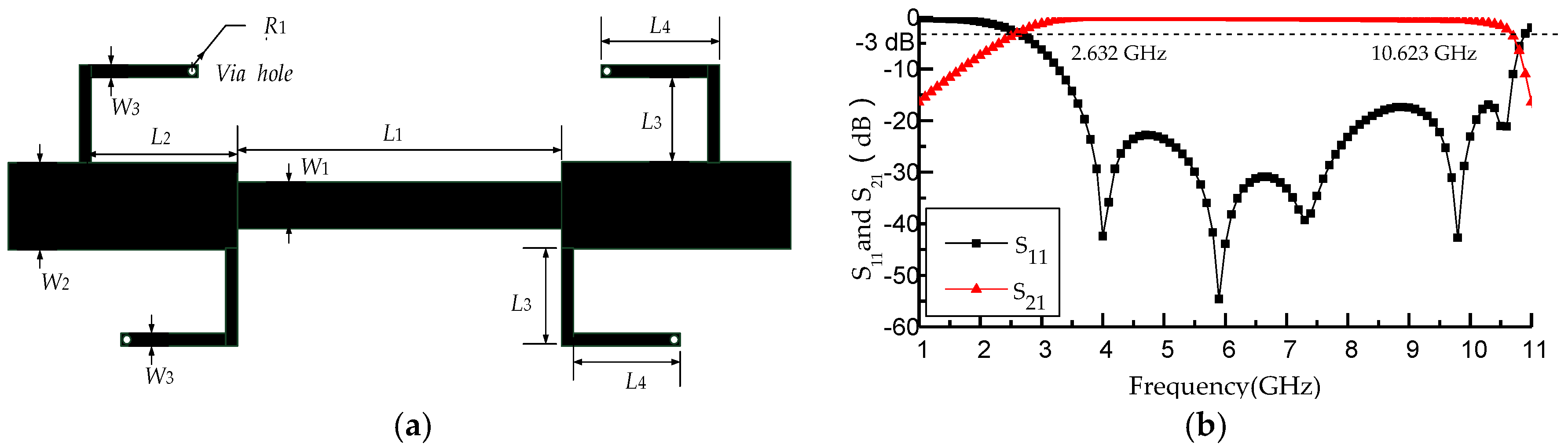
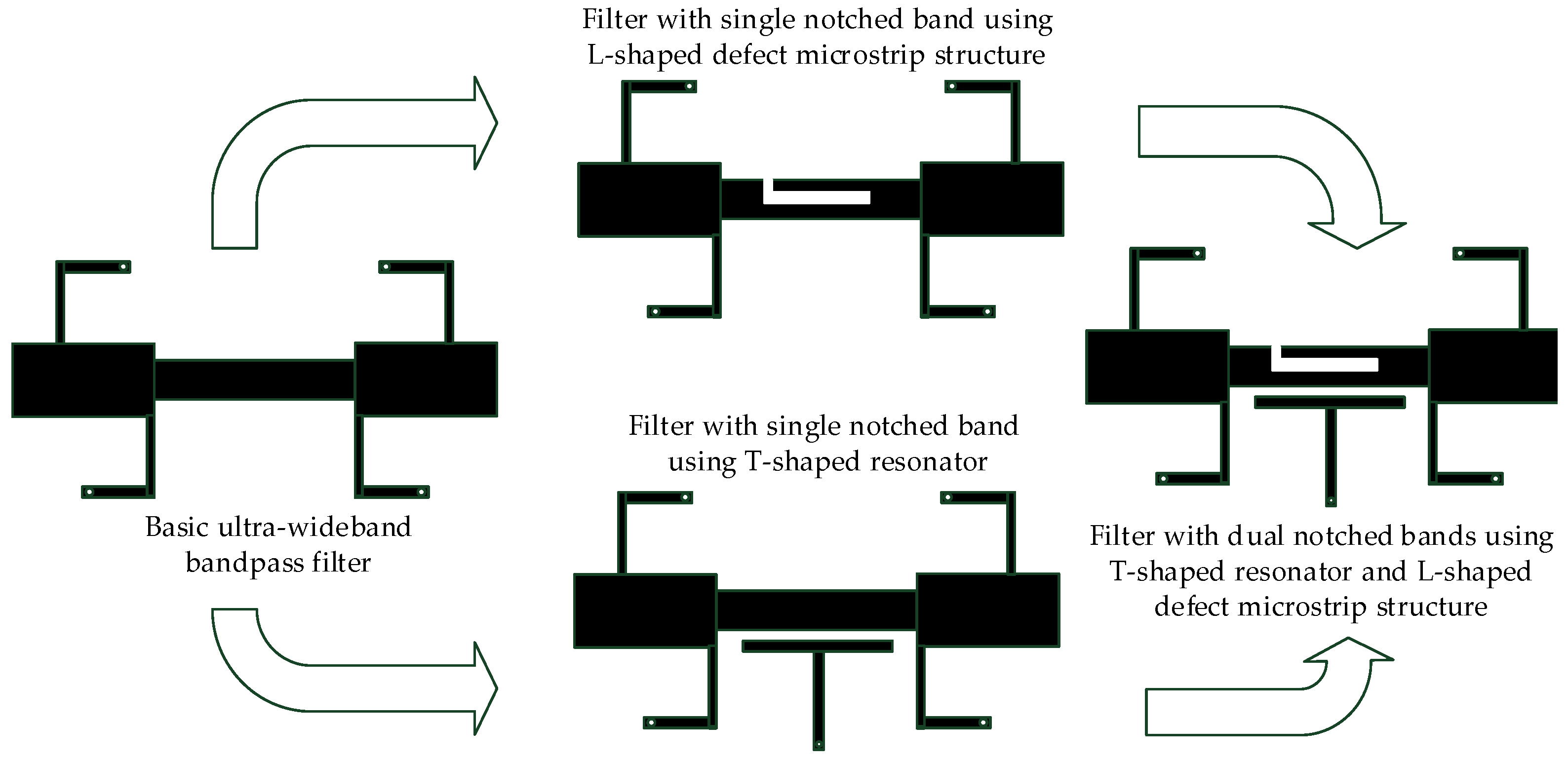
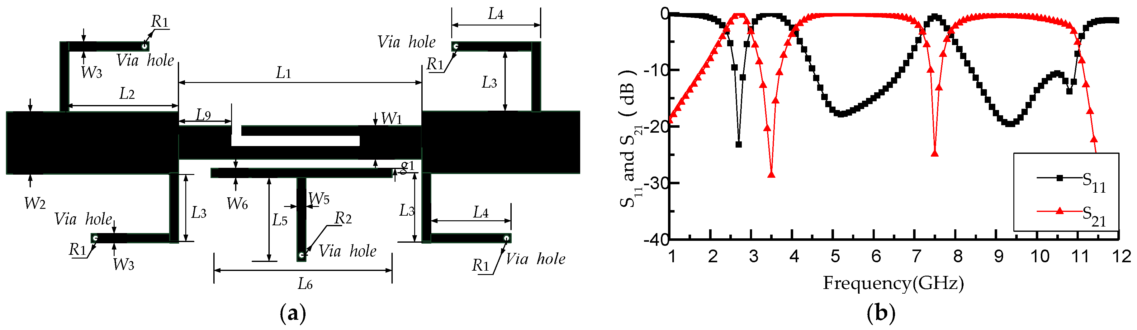
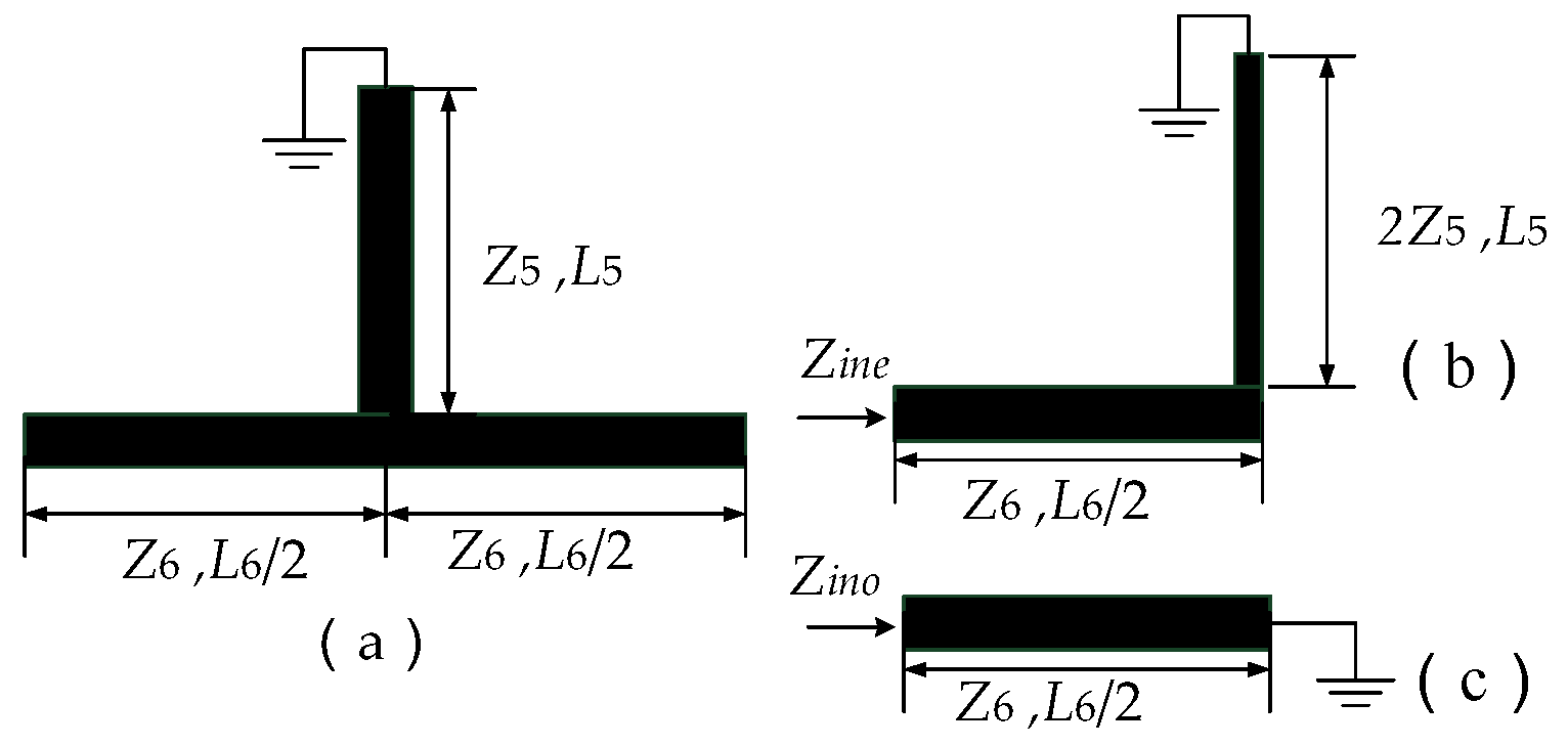
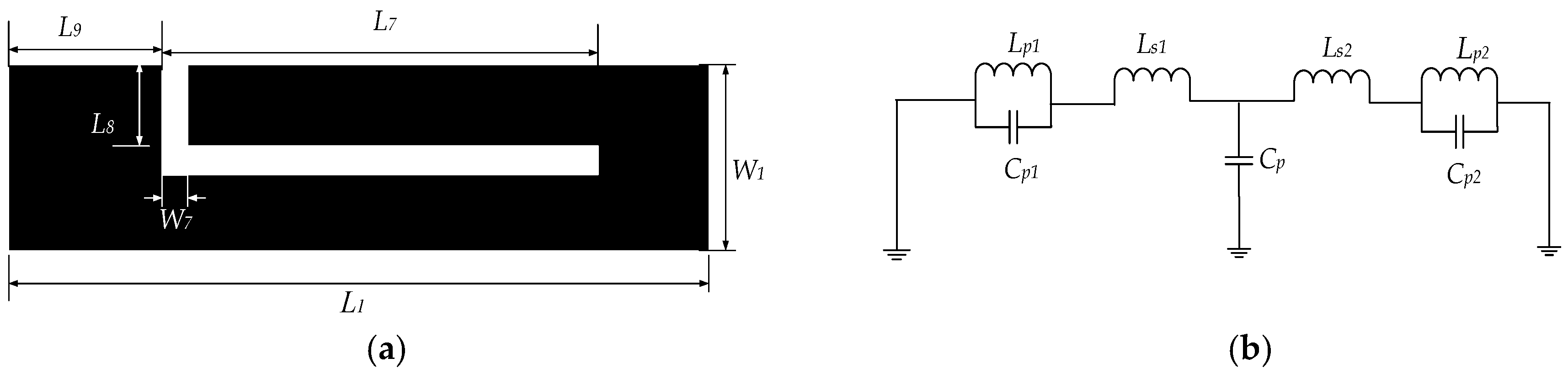
2. Filter Design
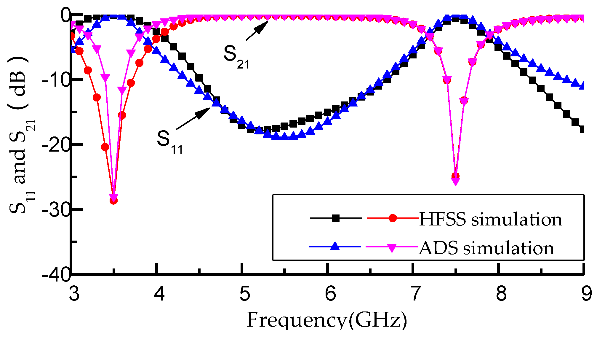
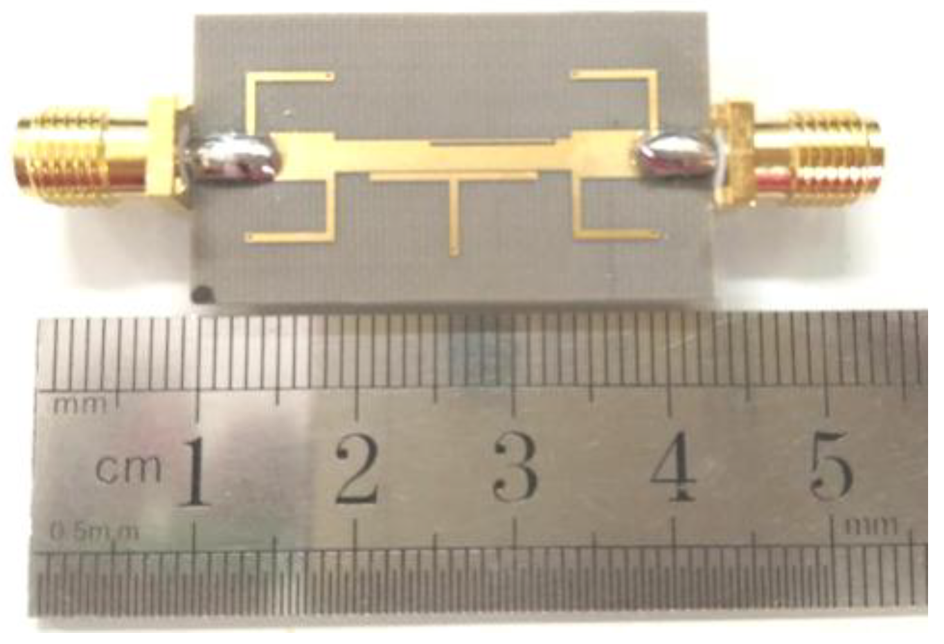
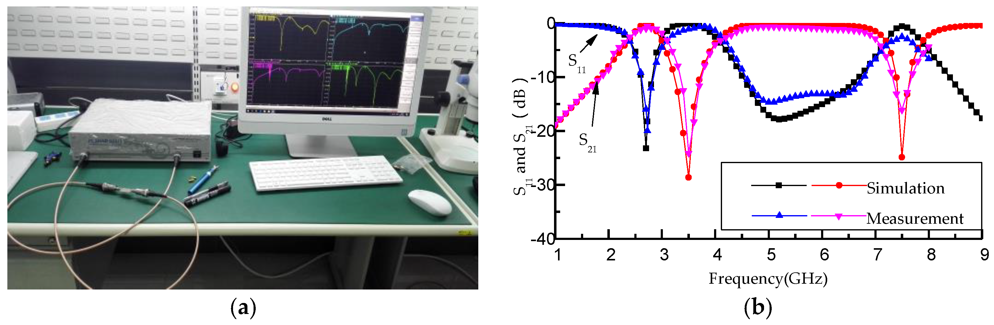
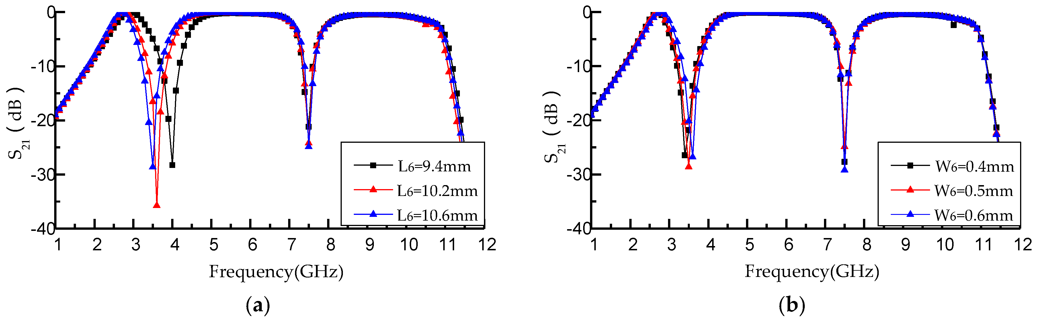
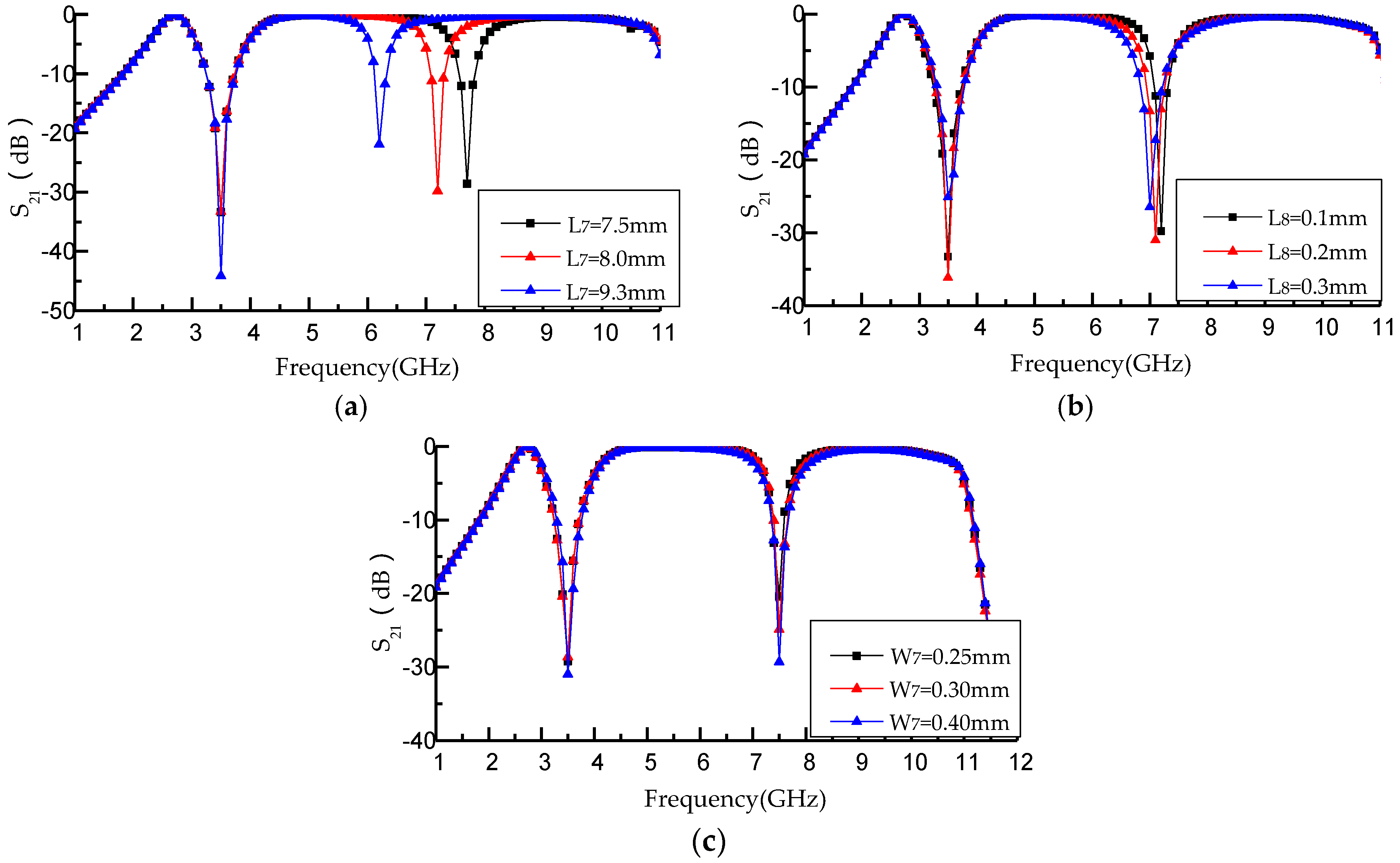
3. Results and Discussion
4. Conclusions
Author Contributions
Acknowledgments
Conflicts of Interest
References
- Federal Communications Commission. Revision of Part 15 of the Commission’s Rules Regarding Ultra-Wideband Transmission Systems; First Note and Order Federal Communications Commission, ET-Docket 98-153; Federal Communications Commission: Washington, DC, USA, 2002. [Google Scholar]
- Wei, F.; Li, W.T.; Shi, X.W.; Huang, Q.L. Compact UWB bandpass filter with triple-notched bands using triple-mode stepped impedance resonator. IEEE Microw. Wirel. Compon. Lett. 2012, 22, 512–514. [Google Scholar] [CrossRef]
- Wei, F.; Qin, P.-Y.; Guo, Y.J.; Shi, X.-W. Design of multi-band bandpass filters based on stub loaded stepped-impedance resonator with defected microstrip structure. IET Microw. Antennas Propag. 2016, 10, 230–236. [Google Scholar] [CrossRef]
- Lu, X.; Wei, B.; Xu, Z.; Cao, B.; Zhang, X.; Wang, R.; Song, F. Superconducting ultra-wideband (UWB) bandpass filter design based on quintuple/quadruple/triple-mode resonator. IEEE Trans. Microw. Theory Tech. 2015, 63, 1281–1293. [Google Scholar] [CrossRef]
- Wei, F.; Wu, Q.Y.; Shi, X.W.; Chen, L. Compact UWB bandpass filter with dual notched bands based on SCRLH resonator. IEEE Microw. Wirel. Compon. Lett. 2011, 21, 28–30. [Google Scholar] [CrossRef]
- Zheng, X.; Liu, W.; Zhang, X.; Jiang, T. Design of dual band-notch UWB bandpass filter based on T-shaped resonator. In Proceedings of the 2016 Progress in Electromagnetic Research Symposium (PIERS), Shanghai, China, 8–11 August 2016; pp. 4482–4486. [Google Scholar]
- Zheng, X.; Jiang, T. Realization of Dual Notch Bands in UWB Bandpass Filter Using Two T-shaped Resonators. In Proceedings of the 2017 International Applied Computational Electromagnetics Society Symposium, Florence, Italy, 26–30 March 2017. [Google Scholar] [CrossRef]
- Zhao, J.; Wang, J.; Zhang, G.; Li, J.-L. Compact microstrip UWB bandpass filter with dual notched bands using E-shaped resonator. IEEE Microw. Wirel. Compon. Lett. 2013, 23, 638–640. [Google Scholar] [CrossRef]
- Zheng, X.; Jiang, T. Design of UWB bandpass filter with dual notched bands using E-shaped resonator. In Proceedings of the IEEE/ACES International Conference on Wireless Information Technology and Systems, Honolulu, HI, USA, 13–18 March 2016; pp. 1–2. [Google Scholar] [CrossRef]
- Zhang, C.; Zhang, J.; Li, L. Triple band-notched UWB antenna based on SIR-DGS and fork-shaped stubs. Electron. Lett. 2014, 50, 67–69. [Google Scholar] [CrossRef]
- Zhou, L.-H.; Ma, Y.; Shi, J.; Chen, J.; Che, W. Differential dual-band bandpass filter with tunable lower band using embedded DGS unit for common-mode suppression. IEEE Trans. Microw. Theory Tech. 2016, 64, 4183–4191. [Google Scholar] [CrossRef]
- Zakaria, Z.; Mutalib, M.A.; Ismail, A.; Isa, M.S.M.; Ismail, M.M.; Latiff, A.A.; Zainuddin, N.A.; Sam, W.Y. Compact structure of band-pass filter integrated with Defected Microstrip Structure (DMS) for wideband applications. In Proceedings of the European Conference on Antennas and Propagation, The Hague, The Netherlands, 6–11 April 2014; Volume 21, pp. 2158–2162. [Google Scholar]
- Wang, J.; Zhao, J.; Li, J.L. Compact UWB bandpass filter with triple notched bands using parallel U-shaped defected microstrip structure. Electron. Lett. 2014, 50, 89–91. [Google Scholar] [CrossRef]
- Yao, B.; Zhou, Y.; Cao, Q. A UWB bandpass filter with multi notched bands using microstrip/coplanar waveguide. In Proceedings of the International Symposium on Antennas, Propagation and EM Theory, Kunming, China, 2–5 November 2008; pp. 637–640. [Google Scholar]
- Mao, S.G.; Chueh, Y.Z.; Chen, C.H.; Hsieh, M.C. Compact ultra-wideband conductor-backed coplanar waveguide bandpass filter with a dual band-notched response. IEEE Microw. Wirel. Compon. Lett. 2009, 19, 149–151. [Google Scholar] [CrossRef]
- Honarvar, M.A.; Sadeghzadeh, R.A. Design of coplanar waveguide ultrawideband bandpass filter using stub-loaded resonator with notched band. Microw. Opt. Technol. Lett. 2012, 54, 2056–2061. [Google Scholar] [CrossRef]
- Senior, D.E.; Cheng, X.; Yong, K.Y. Dual-band filters using complementary split-ring resonator and capacitive loaded half-mode substrate-integrated-waveguide. In Proceedings of the Antennas and Propagation Society International Symposium, Chicago, IL, USA, 8–14 July 2012; pp. 1–2. [Google Scholar]
- Pandey, A.K.; Chauhan, R.K. Miniaturized dual-band BPF for WiMax/WLAN applications. In Proceedings of the IEEE International Conference on Power Electronics, Intelligent Control and Energy Systems, Delhi, India, 4–6 July 2016; pp. 1–4. [Google Scholar]
- Hong, J.S.; Karyamapudi, B.M. A general circuit model for defected ground structures in planar transmission lines. Frequenz 2015, 15, 706–708. [Google Scholar] [CrossRef]
- Wang, J.; Ning, H.; Xiong, Q.; Li, M.; Mao, L.F. A novel miniaturized dual-band bandstop filter using dual-plane defected structures. Prog. Electromagn. Res. 2013, 134, 397–417. [Google Scholar] [CrossRef]
- Gupta, K.C.; Garg, R.; Bahl, I.; Bhartia, P. Microstrip Lines and Slotlines, 2nd ed.; Artech House: Norwood, MA, USA, 1996. [Google Scholar]
- Wang, K.; Wong, S.W.; Chu, Q.X. A compact UWB CPW bandpass filter with short-ended H-shaped resonator and controllable notched band. Microw. Opt. Technol. Lett. 2013, 55, 1577–1581. [Google Scholar] [CrossRef]
- Nosrati, M.; Daneshmand, M. Compact microstrip ultra-wideband double/single notch-band band-pass filter based on wave’s cancellation theory. Microw. Antennas Propag. Lett. 2012, 6, 862–868. [Google Scholar] [CrossRef]
- Song, K.; Xue, Q. Asymmetric dual-line coupling structure for multiple-notch implementation in UWB bandpass filters. Electron. Lett. 2010, 46, 1388–1390. [Google Scholar] [CrossRef]
- Wang, H.; Tam, K.W.; Ho, S.K.; Kang, W.; Wu, W. Design of ultra-wideband bandpass filters with fixed and reconfigurable notch bands using terminated cross-shaped resonators. IEEE Trans. Microw. Theory Tech. 2014, 62, 252–265. [Google Scholar] [CrossRef]
- Lung, C.K.; Chin, K.S.; Fu, J.S. Tri-section stepped-impedance resonators for design of dual-band bandstop filter. In Proceedings of the European Microwave Conference, Rome, Italy, 29 September–1 October 2009; pp. 771–774. [Google Scholar]
- Chen, F.C.; Qiu, J.M.; Chu, Q.-X. Dual-band bandstop filter using stub-loaded resonators with sharp rejection characteristic. Electron. Lett. 2013, 49, 351–352. [Google Scholar] [CrossRef]
- Gao, L.; Cai, S.W.; Zhang, X.Y.; Xue, Q. Dual-band bandstop filter using open and short stub-loaded resonators. In Proceedings of the International Conference on Microwave and Millimeter Wave Technology, Shenzhen, China, 5–8 May 2012; Volume 4, pp. 1–3. [Google Scholar]
- Feng, W.J.; Che, W.Q.; Shi, S.Y.; Xue, Q. Compact dual-wideband bandstop filters based on open-coupled lines and transversal signal-interaction concepts. IET Microw. Antennas Propag. 2013, 7, 92–97. [Google Scholar] [CrossRef]
- Peng, H.; Luo, Y.; Zhao, J. Compact microstrip UWB bandpass filter with two band-notches for UWB applications. Prog. Electromagn. Res. Lett. 2014, 45, 25–30. [Google Scholar] [CrossRef]
- Tilanthe, P.; Sharma, P.C.; Bandopadhyay, T.K. A monopole microstrip antenna with enhanced dual band rejection for UWB applications. Prog. Electromagn. Res. B 2012, 38, 315–331. [Google Scholar] [CrossRef]


| C (pF) | L (nH) |
|---|---|
| Cp1 = 2.415 | Lp1 = 0.85 |
| Cp = 2.489 | Ls1 = 0.18 |
| Cp2 = 0.1216 | Ls2 = −0.105 |
| -- | Lp2 = 0.47 |
| Length | Length | Width | Width | Radius | Gap Length |
|---|---|---|---|---|---|
| L1 = 15 | L5 = 5.3 | W1 = 1.95 | W5 = 0.5 | R1 = 0.15 | g1 = 0.1 |
| L2 = 5 | L6 = 10.6 | W2 = 3 | W6 = 0.3 | R2 = 0.15 | -- |
| L3 = 4 | L7 = 9 | W3 = 0.3 | W7 = 0.1 | -- | -- |
| L3 = 4 | L8 = 0.1 | W4 = 1.4 | W8 = 0.3 | -- | -- |
| Notch Frequency (GHz) | 3 dB Bandwidth (GHz) | Fractional Bandwidths (FBW) % | Rejection Level (dB) |
|---|---|---|---|
| 3.5 | 1.07 | 15.62 | 28.6 |
| 7.5 | 0.61 | 8.91 | 25.1 |
| Notch Frequency (GHz) | 3 dB Bandwidth (GHz) | Fractional Bandwidths (FBW) % | Rejection Level (dB) |
|---|---|---|---|
| 3.5 | 1.09 | 15.91 | 25.2 |
| 7.5 | 0.66 | 9.63 | 17.3 |
| Ref. | Insertion Loss (dB) | Return Loss (dB) | fL(GHz) | fH (GHz) | Fractional Bandwidths (FBW) % |
|---|---|---|---|---|---|
| [22] | 0.5 | 13 | 5.5 | 13.6 | 112 |
| [23] | 0.6 | 12 | 6.55 | 8.66 | 130 |
| [24] | 0.65 | 10 | 4.9 | 8.5 | 110 |
| [25] | 1.2 | 11 | 4.3 | 9.1 | 82.4 |
| [26] | 1.1 | 10 | 2.4 | 5.5 | 110 |
| [27] | 1.5 | 15 | 2.4 | 5.2 | 105 |
| [28] | 0.7 | 15 | 1.16 | 3.5 | 95.5 |
| [29] | 1.1 | 15 | 2.62 | 5.32 | 105 |
| [30] | 2 | 15 | 5.8 | 8 | 92 |
| [31] | 1.12 | 11 | 2.4 | 5.2 | 89.6 |
| This work | 0.8 | 15.5 | 3.5 | 7.5 | 123.9 |
© 2018 by the authors. Licensee MDPI, Basel, Switzerland. This article is an open access article distributed under the terms and conditions of the Creative Commons Attribution (CC BY) license (http://creativecommons.org/licenses/by/4.0/).
Share and Cite
Zheng, X.; Pan, Y.; Jiang, T. UWB Bandpass Filter with Dual Notched Bands Using T-Shaped Resonator and L-Shaped Defected Microstrip Structure. Micromachines 2018, 9, 280. https://doi.org/10.3390/mi9060280
Zheng X, Pan Y, Jiang T. UWB Bandpass Filter with Dual Notched Bands Using T-Shaped Resonator and L-Shaped Defected Microstrip Structure. Micromachines. 2018; 9(6):280. https://doi.org/10.3390/mi9060280
Chicago/Turabian StyleZheng, Xuemei, Yuwen Pan, and Tao Jiang. 2018. "UWB Bandpass Filter with Dual Notched Bands Using T-Shaped Resonator and L-Shaped Defected Microstrip Structure" Micromachines 9, no. 6: 280. https://doi.org/10.3390/mi9060280
APA StyleZheng, X., Pan, Y., & Jiang, T. (2018). UWB Bandpass Filter with Dual Notched Bands Using T-Shaped Resonator and L-Shaped Defected Microstrip Structure. Micromachines, 9(6), 280. https://doi.org/10.3390/mi9060280