Acquisition of Neural Action Potentials Using Rapid Multiplexing Directly at the Electrodes


Abstract
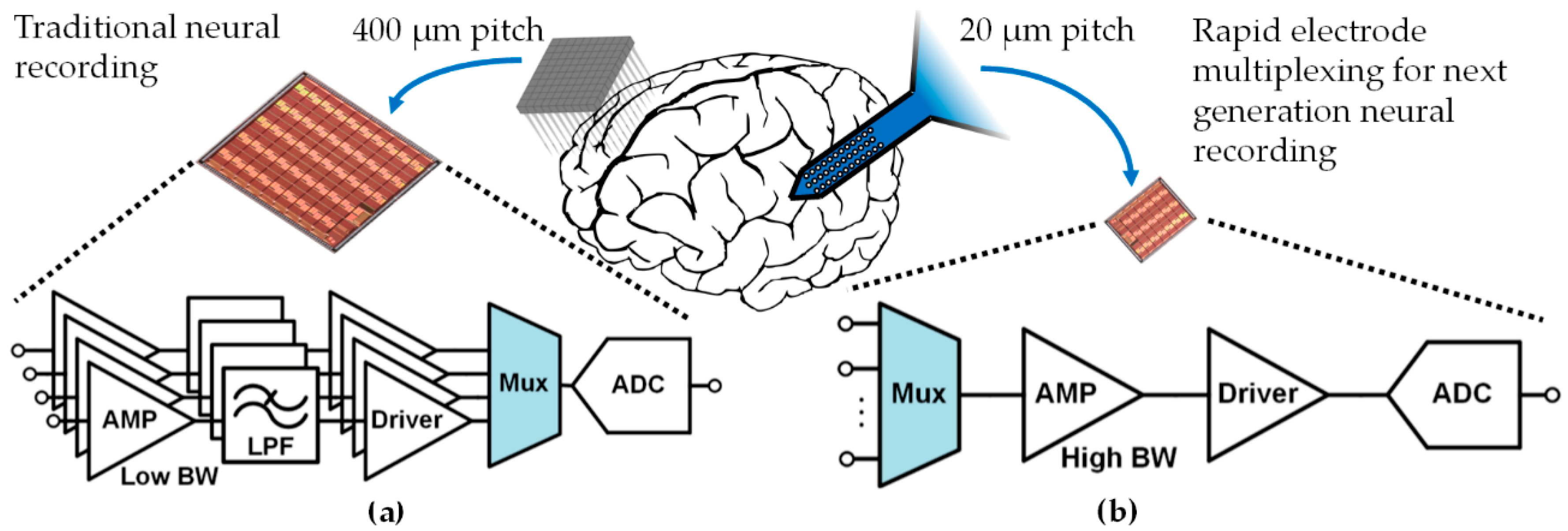
1. Introduction
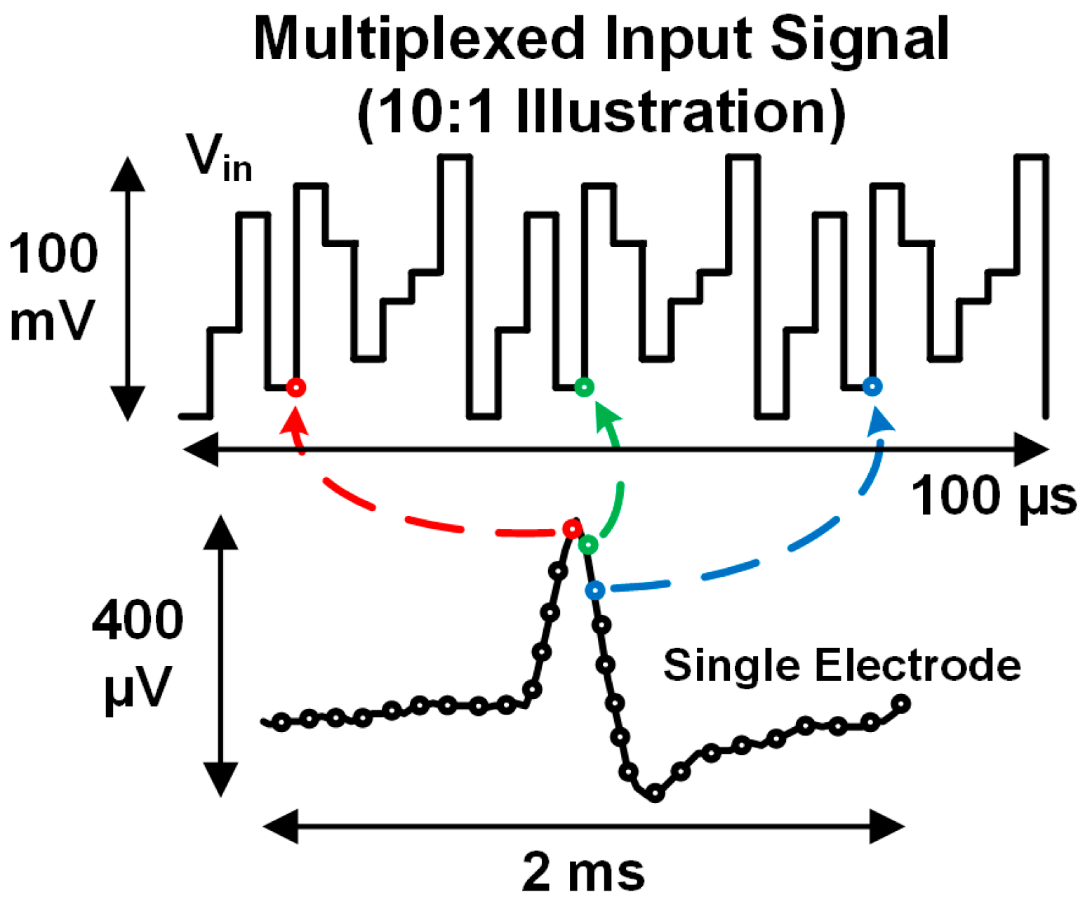
2. Rapidly Multiplexed Neural Recording: Theory and Practical Issues
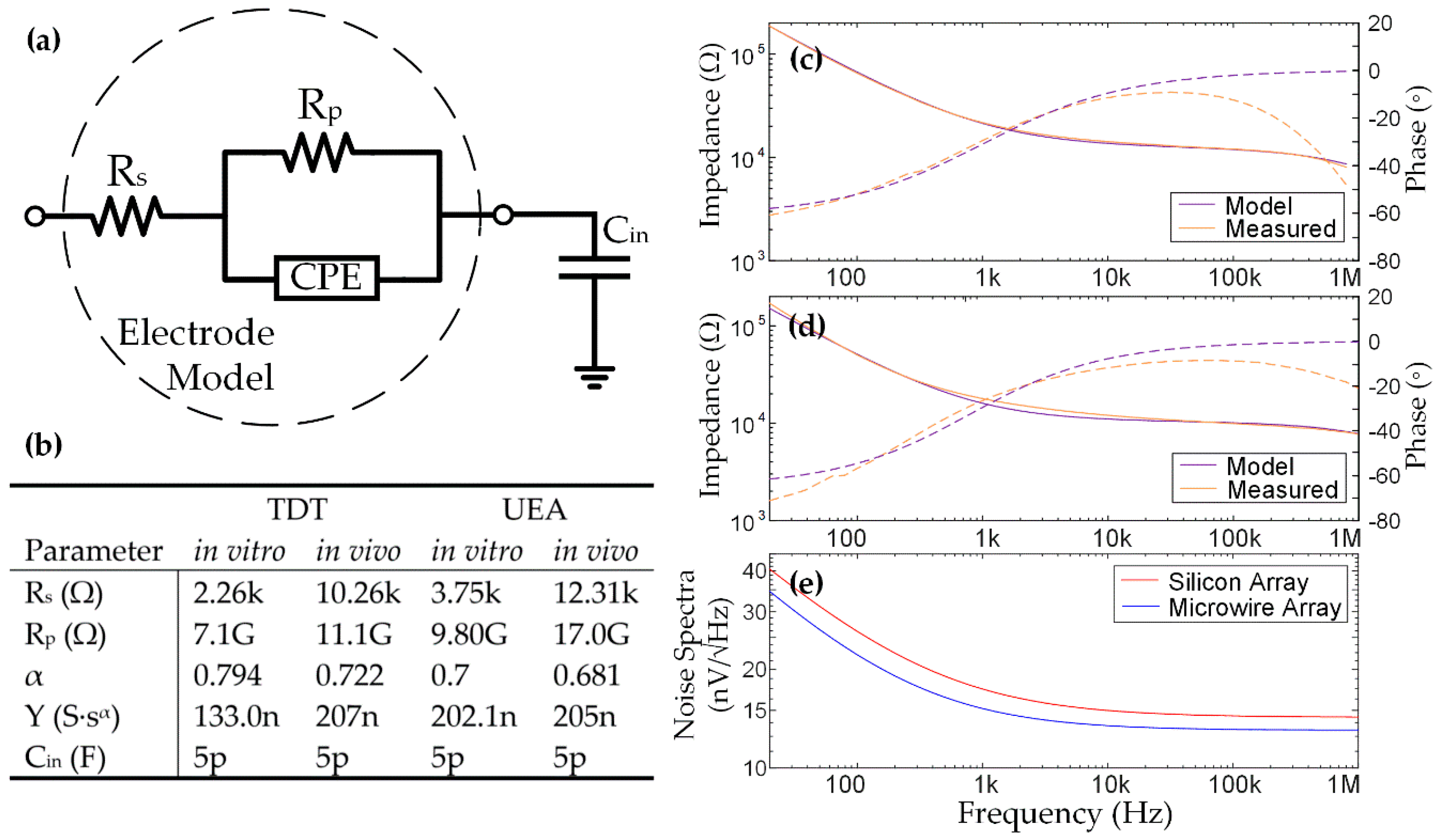
2.1. DC Offsets from the Electrodes
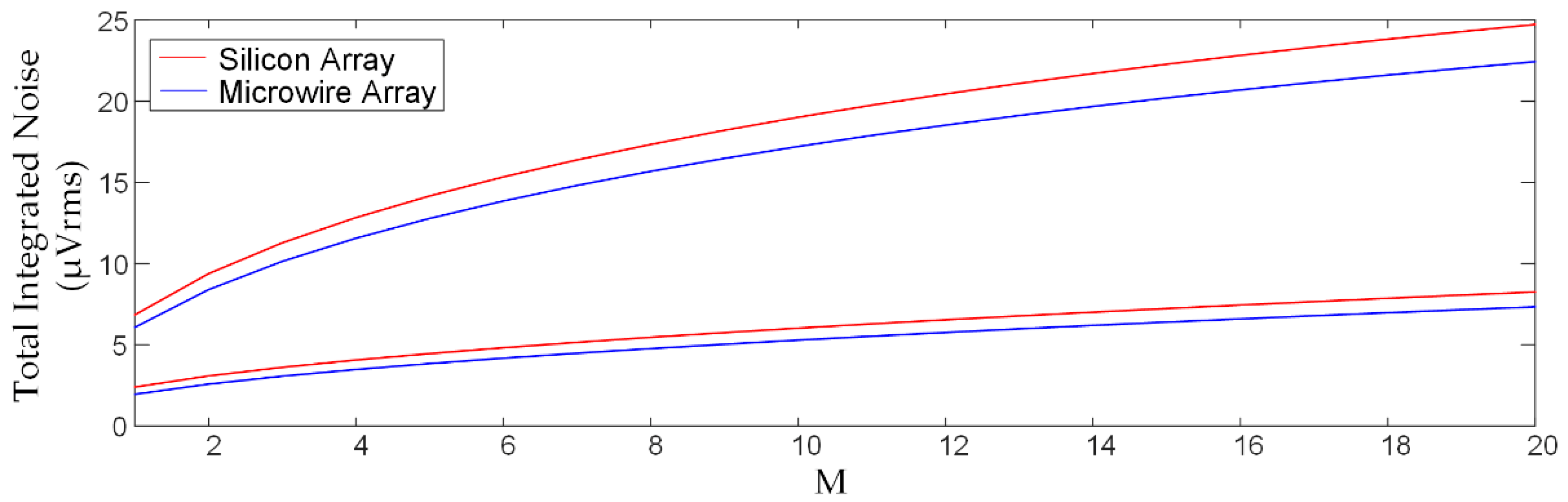
2.2. Noise from Acquisition Electronics
2.3. Noise from the Electrodes
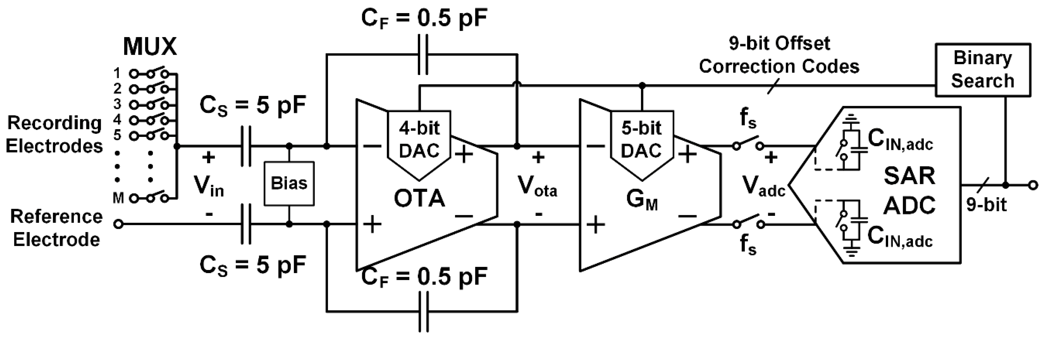
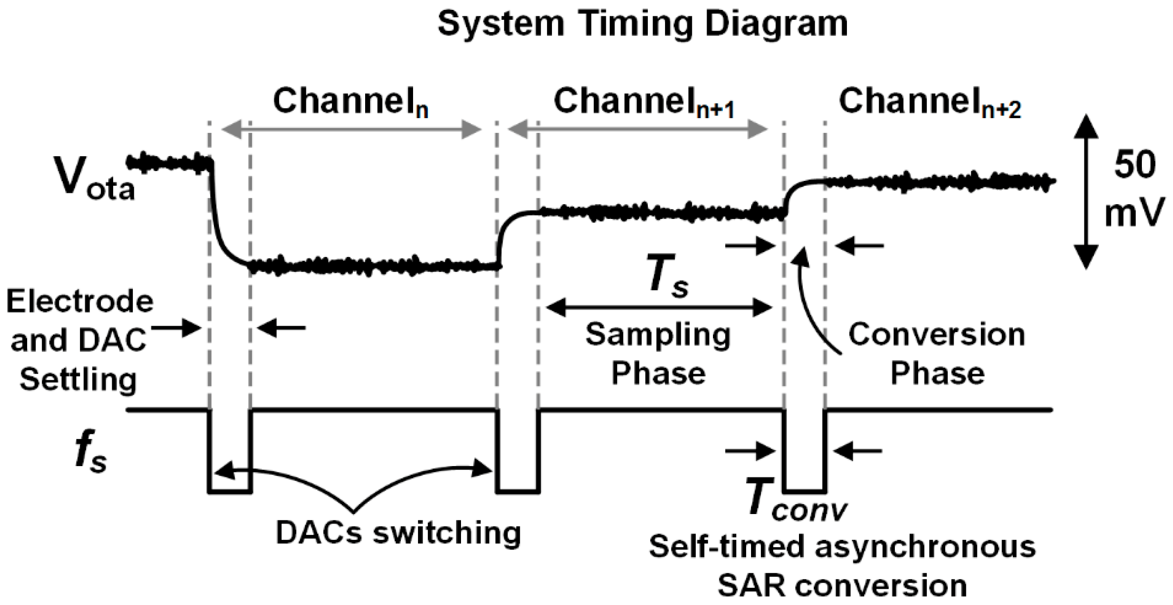
3. Rapidly Multiplexed Neural Recording Circuit Architecture
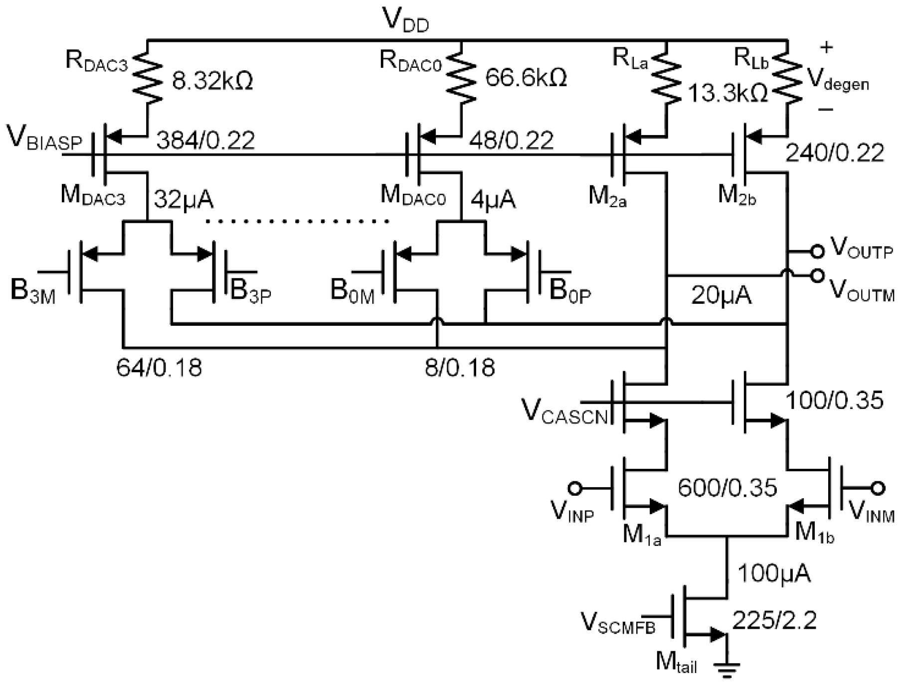
3.1. LNA Design
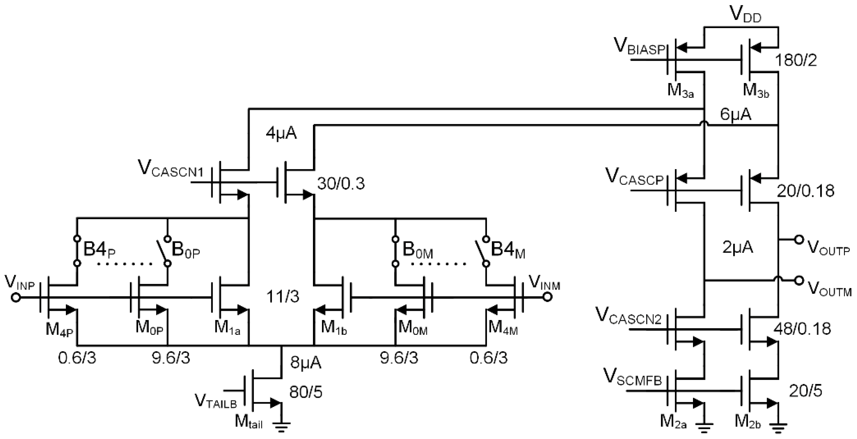
3.2. Transconductance Amplifier Design
3.3. SAR ADC Design
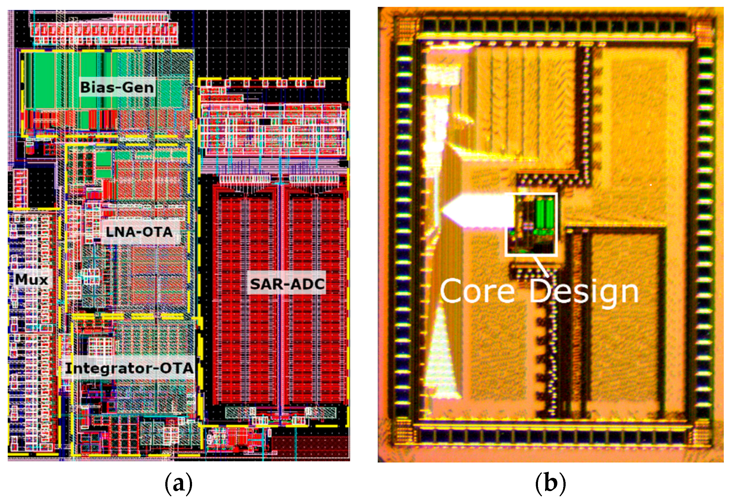
4. Experimental Results
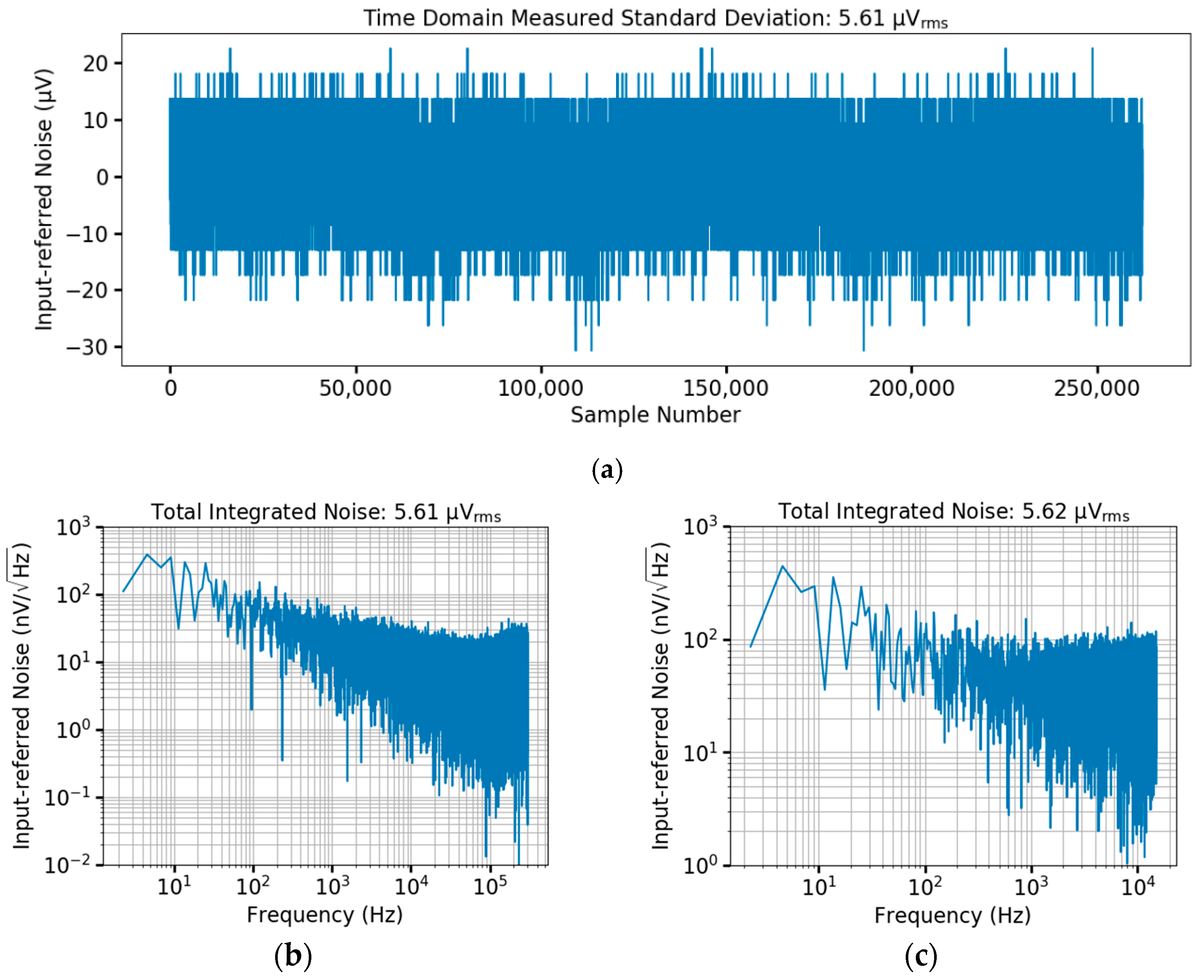
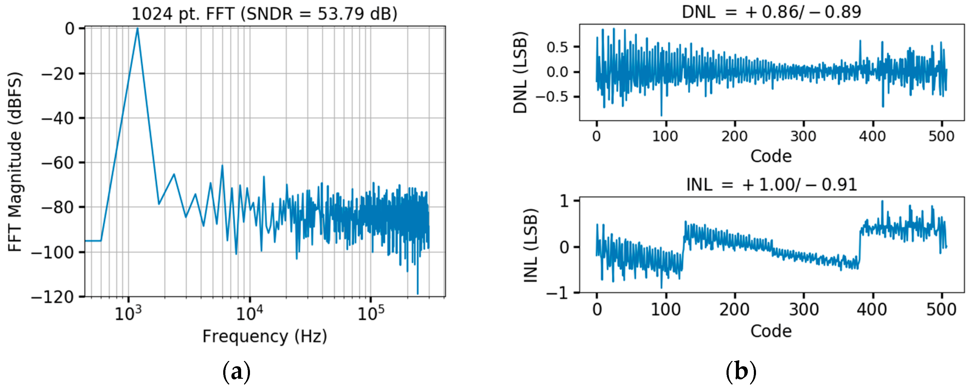
4.1. Bench Testing of the CMOS Prototype
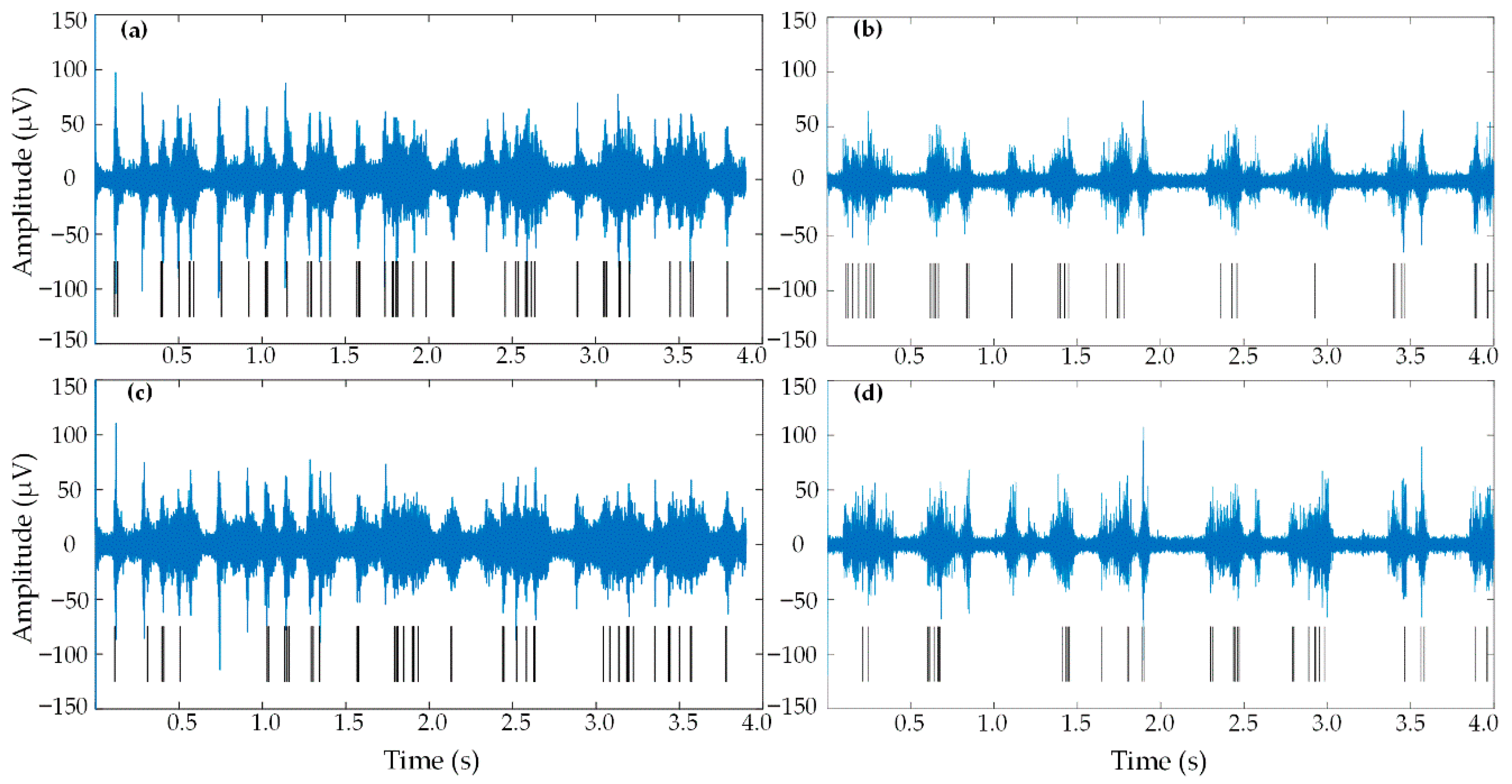
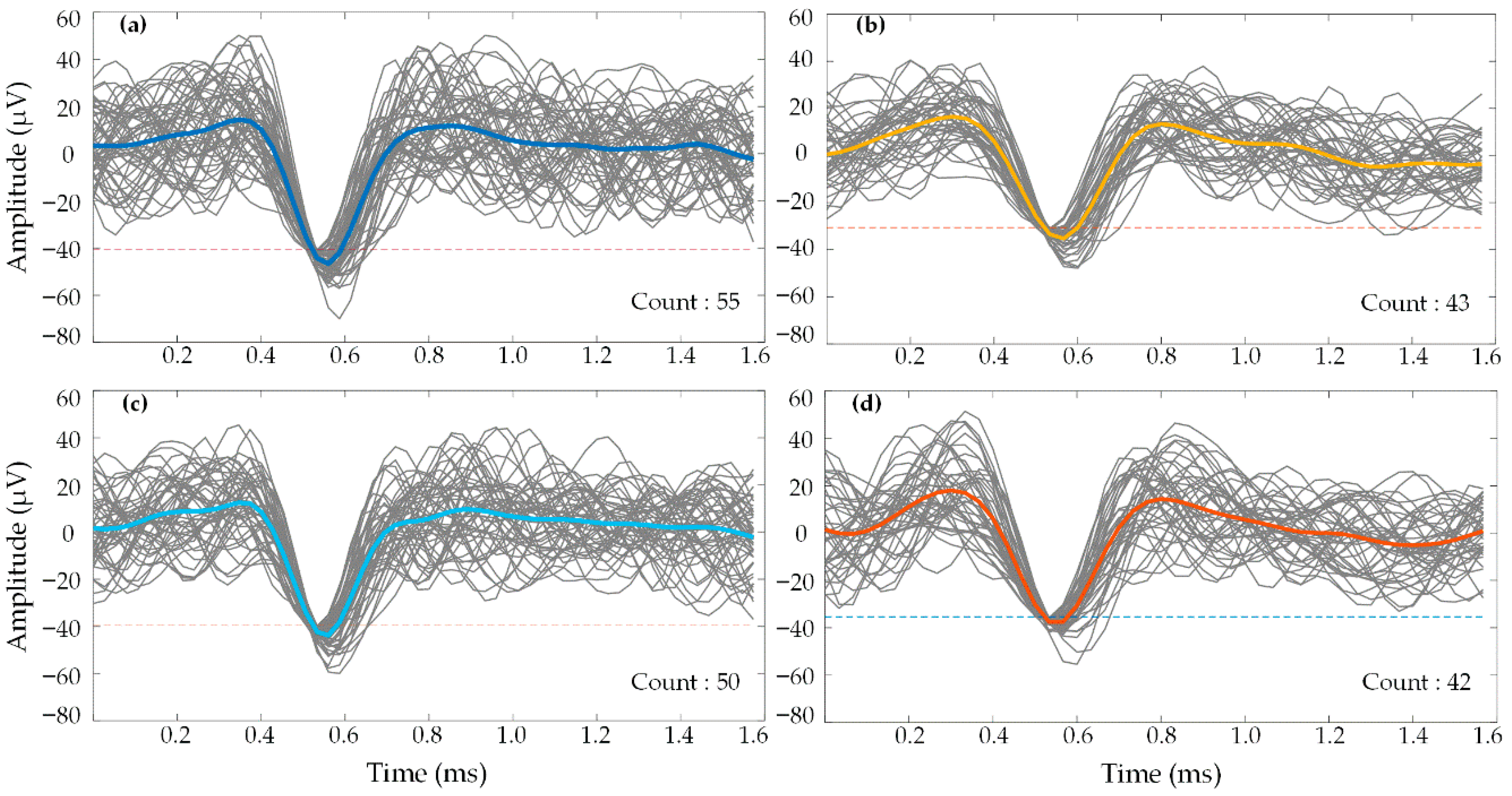
4.2. In Vivo Testing of the CMOS Prototype
5. Discussion
Author Contributions
Funding
Acknowledgments
Conflicts of Interest
References
- Gunasekera, B.; Saxena, T.; Bellamkonda, R.; Karumbaiah, L. Intracortical Recording Interfaces: Current Challenges to Chronic Recording Function. ACS Chem. Neurosci. 2015, 6, 68–83. [Google Scholar] [CrossRef] [PubMed]
- Marblestone, A.H.; Zamft, B.M.; Maguire, Y.G.; Shapiro, M.G.; Cybulski, T.R.; Glaser, J.I.; Amodei, D.; Stranges, P.B.; Kalhor, R.; Dalrymple, D.A.; et al. Physical Principles for Scalable Neural Recording. Front. Comput. Neurosci. 2013, 7, 1–34. [Google Scholar] [CrossRef] [PubMed]
- Schwarz, D.A.; Lebedev, M.A.; Hanson, T.L.; Dimitrov, D.F.; Lehew, G.; Meloy, J.; Rajangam, S.; Subramanian, V.; Ifft, P.J.; Li, Z.; et al. Chronic, Wireless Recordings of Large-Scale Brain Activity in Freely Moving Rhesus Monkeys. Nat. Methods 2014, 11, 670–676. [Google Scholar] [CrossRef] [PubMed]
- Yin, M.; Borton, D.A.; Komar, J.; Agha, N.; Lu, Y.; Li, H.; Laurens, J.; Lang, Y.; Li, Q.; Bull, C.; et al. Wireless Neurosensor for Full-Spectrum Electrophysiology Recordings during Free Behavior. Neuron 2014, 84, 1170–1182. [Google Scholar] [CrossRef] [PubMed]
- Foster, J.D.; Nuyujukian, P.; Freifeld, O.; Gao, H.; Walker, R.; Ryu, S.I.; Meng, T.H.; Murmann, B.; Black, M.J.; Shenoy, K.V. A Freely-Moving Monkey Treadmill Model. J. Neural Eng. 2014, 11, 046020. [Google Scholar] [CrossRef] [PubMed]
- Hochberg, L.R.; Serruya, M.D.; Friehs, G.M.; Mukand, J.A.; Saleh, M.; Caplan, A.H.; Branner, A.; Chen, D.; Penn, R.D.; Donoghue, J.P. Neuronal Ensemble Control of Prosthetic Devices by a Human with Tetraplegia. Nature 2006, 442, 164–171. [Google Scholar] [CrossRef] [PubMed]
- Collinger, J.L.; Wodlinger, B.; Downey, J.E.; Wang, W.; Tyler-Kabara, E.C.; Weber, D.J.; McMorland, A.J.C.; Velliste, M.; Boninger, M.L.; Schwartz, A.B. High-Performance Neuroprosthetic Control by an Individual with Tetraplegia. Lancet 2013, 381, 557–564. [Google Scholar] [CrossRef]
- Gilja, V.; Pandarinath, C.; Blabe, C.H.; Nuyujukian, P.; Simeral, J.D.; Sarma, A.A.; Sorice, B.L.; Perge, J.A.; Jarosiewicz, B.; Hochberg, L.R.; et al. Clinical Translation of a High-Performance Neural Prosthesis. Nat. Med. 2015, 21, 1142–1145. [Google Scholar] [CrossRef] [PubMed]
- Stevenson, I.H.; Kording, K.P. How Advances in Neural Recording Affect Data Analysis. Nat. Neurosci. 2011, 14, 139–142. [Google Scholar] [CrossRef] [PubMed]
- Rajkowska, G.; Halaris, A.; Selemon, L.D. Reductions in Neuronal and Glial Density Characterize the DL PFC Cortex in Bipolar Disorder. Biol. Psychiatry 2001, 49, 741–752. [Google Scholar] [CrossRef]
- Khodagholy, D.; Gelinas, J.N.; Thesen, T.; Doyle, W.; Devinsky, O.; Malliaras, G.G.; Buzsáki, G. NeuroGrid: Recording Action Potentials from the Surface of the Brain. Nat. Neurosci. 2015, 18, 310–315. [Google Scholar] [CrossRef] [PubMed]
- Rios, G.; Lubenov, E.V.; Chi, D.; Roukes, M.L.; Siapas, A.G. Nanofabricated Neural Probes for Dense 3-D Recordings of Brain Activity. Nano Lett. 2016, 16, 6857–6862. [Google Scholar] [CrossRef] [PubMed]
- Berenyi, A.; Somogyvari, Z.; Nagy, A.J.; Roux, L.; Long, J.D.; Fujisawa, S.; Stark, E.; Leonardo, A.; Harris, T.D.; Buzsaki, G. Large-Scale, High-Density (up to 512 Channels) Recording of Local Circuits in Behaving Animals. J. Neurophysiol. 2014, 111, 1132–1149. [Google Scholar] [CrossRef] [PubMed]
- Chung, J.E.; Joo, H.R.; Fan, J.L.; Liu, D.F.; Barnett, A.H.; Chen, S.; Geaghan-Breiner, C.; Karlsson, M.P.; Karlsson, M.; Lee, K.Y.; et al. High-Density, Long-Lasting, and Multi-Region Electrophysiological Recordings Using Polymer Electrode Arrays. bioRxiv 2018. [Google Scholar] [CrossRef]
- Jun, J.J.; Steinmetz, N.A.; Siegle, J.H.; Denman, D.J.; Bauza, M.; Barbarits, B.; Lee, A.K.; Anastassiou, C.A.; Andrei, A.; Aydin, Ç.; et al. Fully Integrated Silicon Probes for High-Density Recording of Neural Activity. Nature 2017, 551, 232–236. [Google Scholar] [CrossRef] [PubMed]
- Barrese, J.C.; Rao, N.; Paroo, K.; Triebwasser, C.; Vargas-Irwin, C.; Franquemont, L.; Donoghue, J.P. Failure Mode Analysis of Silicon-Based Intracortical Microelectrode Arrays in Non-Human Primates. J. Neural Eng. 2013, 10, 66014. [Google Scholar] [CrossRef] [PubMed]
- Bharucha, E.; Sepehrian, H.; Gosselin, B. A Survey of Neural Front End Amplifiers and Their Requirements toward Practical Neural Interfaces. J. Low Power Electron. Appl. 2014, 4, 268–291. [Google Scholar] [CrossRef]
- Smith, W.A.; Uehlin, J.P.; Perlmutter, S.I.; Rudell, J.C.; Sathe, V.S. A Scalable, Highly-Multiplexed Delta-Encoded Digital Feedback ECoG Recording Amplifier with Common and Differential-Mode Artifact Suppression. In 2017 Symposium on VLSI Circuits, Proceedings of the 2017 Symposium on VLSI Circuits, Kyoto, Japan, 5–8 June 2017; IEEE: Piscataway, NJ, USA, 2017; pp. C172–C173. [Google Scholar]
- Viventi, J.; Kim, D.-H.; Vigeland, L.; Frechette, E.S.; Blanco, J.A.; Kim, Y.-S.; Avrin, A.E.; Tiruvadi, V.R.; Hwang, S.-W.; Vanleer, A.C.; et al. Flexible, Foldable, Actively Multiplexed, High-Density Electrode Array for Mapping Brain Activity In Vivo. Nat. Neurosci. 2011, 14, 1599–1605. [Google Scholar] [CrossRef] [PubMed]
- Guo, J.; Ng, W.; Yuan, J.; Li, S.; Chan, M. A 200-Channel Area-Power-Efficient Chemical and Electrical Dual-Mode Acquisition IC for the Study of Neurodegenerative Diseases. IEEE Trans. Biomed. Circuits Syst. 2016, 10, 567–578. [Google Scholar] [CrossRef] [PubMed]
- Zou, X.; Liu, L.; Cheong, J.H.; Yao, L.; Li, P.; Cheng, M.; Goh, W.L.; Rajkumar, R.; Dawe, G.S.; Cheng, K.-W.; et al. A 100-Channel 1-mW Implantable Neural Recording IC. IEEE Trans. Biomed. Circuits Syst. I 2013, 60, 2584–2596. [Google Scholar] [CrossRef]
- Lee, J.; Rhew, H.G.; Kipke, D.R.; Flynn, M.P. A 64 Channel Programmable Closed-Loop Neurostimulator with 8 Channel Neural Amplifier and Logarithmic ADC. IEEE J. Solid State Circuits 2010, 45, 1935–1945. [Google Scholar] [CrossRef]
- Chae, M.S.; Yang, Z.; Yuce, M.R.; Hoang, L.; Liu, W. A 128-Channel 6 mW Wireless Neural Recording IC with Spike Feature Extraction and UWB Transmitter. IEEE Trans. Neural Syst. Rehabil. Eng. 2009, 17, 312–321. [Google Scholar] [CrossRef] [PubMed]
- Mohseni, P.; Najafi, K.; Eliades, S.J.; Wang, X. Wireless Multichannel Biopotential Recording Using an Integrated FM Telemetry Circuit. IEEE Trans. Neural Syst. Rehabil. Eng. 2005, 13, 263–271. [Google Scholar] [CrossRef] [PubMed]
- Wise, K.D.; Anderson, D.J.; Hetke, J.F.; Kipke, D.R.; Najafi, K. Wireless Implantable Microsystems: High-Density Electronic Interfaces to the Nervous System. Proc. IEEE 2004, 92, 76–97. [Google Scholar] [CrossRef]
- Bai, Q.; Wise, K.D. Single-Unit Neural Recording with Active Microelectrode Arrays. IEEE Trans. Biomed. Eng. 2001, 48, 911–920. [Google Scholar] [CrossRef] [PubMed]
- Cogan, S.F. Neural Stimulation and Recording Electrodes. Annu. Rev. Biomed. Eng. 2008, 10, 275–309. [Google Scholar] [CrossRef] [PubMed]
- Muller, R.; Gambini, S.; Rabaey, J.M. A 0.013 mm2, 5 mW, DC-Coupled Neural Signal Acquisition IC with 0.5 V Supply. IEEE J. Solid State Circuits 2012, 47, 232–243. [Google Scholar] [CrossRef]
- Shulyzki, R.; Abdelhalim, K.; Bagheri, A.; Salam, M.T.; Florez, C.M.; Velazquez, J.L.P.; Carlen, P.L.; Genov, R. 320-Channel Active Probe for High-Resolution Neuromonitoring and Responsive Neurostimulation. IEEE Trans. Biomed. Circuits Syst. 2015, 9, 34–49. [Google Scholar] [CrossRef] [PubMed]
- Harrison, R.R.; Watkins, P.T.; Lovejoy, R.; Kier, R.; Black, D.J.; Greger, B.; Solzbacher, F. A Low-Power Integrated Circuit for a Wireless 100- Electrode Neural Recording System. IEEE J. Solid State Circuits 2007, 42, 123–133. [Google Scholar] [CrossRef]
- Gao, H.; Walker, R.M.; Nuyujukian, P.; Makinwa, K.A.A.; Shenoy, K.V.; Murmann, B.; Meng, T.H. HermesE: A 96-Channel Full Data Rate Direct Neural Interface in 0.13 µm CMOS. IEEE J. Solid State Circuits 2012, 47, 1043–1055. [Google Scholar] [CrossRef]
- Vittoz, E.A. Weak Inversion for Ultra Low-Power and Very Low-Voltage Circuits. In Proceedings of the 2009 IEEE Asian Solid State Circuits Conference, Taipei, Taiwan, 16–18 November 2009; IEEE: Piscataway, NJ, USA, 2009. [Google Scholar] [CrossRef]
- Fee, M.S.; Mitra, P.P.; Kleinfeld, D. Variability of Extracellular Spike Waveforms of Cortical Neurons. J. Neurophysiol. 1996, 76, 3823–3833. [Google Scholar] [CrossRef] [PubMed]
- Mirzaei, A.; Chehrazi, S.; Bagheri, R.; Abidi, A.A. Analysis of First-Order Anti-Aliasing Integration Sampler. IEEE Trans. Circuits Syst. I 2008, 55, 2994–3005. [Google Scholar] [CrossRef]
- Poberezhskiy, Y.; Poberezhskiy, G. Sampling with Weighted Integration for Digital Receivers. In Proceedings of the 1999 IEEE MTT-S International Topical Symposium on Technologies for Wireless Applications, Vancouver, BC, Canada, 21–24 February 1999; IEEE: Piscataway, NJ, USA. [Google Scholar] [CrossRef]
- Chang, J.; Abidi, A.A.; Viswanathan, C.R. Flicker Noise in CMOS Transistors from Subthreshold to Strong Inversion at Various Temperatures. IEEE Trans. Electron. Devices 1994, 41, 1965–1971. [Google Scholar] [CrossRef]
- Gardner, A.T.; Strathman, H.J.; Warren, D.J.; Walker, R.M. Signal and Noise Sources from TDT Microwire Arrays Implanted in Rodent Cortex. IEEE Life Sci. Conf. 2018. accepted. [Google Scholar]
- Gardner, A.T.; Strathman, H.J.; Warren, D.J.; Walker, R.M. Impedance and Noise Characterizations of Utah and Microwire Electrode Arrays. IEEE J. Electromagn. RF Microwaves Med. Biol. 2018, 2, 1–8. [Google Scholar]
- Gardner, A.T.; Mize, J.; Warren, D.J.; Walker, R.M. Comparative Characterization of in vivo and in vitro Noise of the SIROF Utah Electrode Array. In Proceedings of the 2017 IEEE SENSORS, Glasgow, UK, 29 October–1 November 2017; IEEE: Piscataway, NJ, USA, 2007. [Google Scholar] [CrossRef]
- Sharma, M.; Gardner, A.T.; Silver, J.; Walker, R.M. Noise and Impedance of the SIROF Utah Electrode Array. In Proceedings of the 2016 IEEE SENSORS, Orlando, FL, USA, 30 October–3 November 2016; IEEE: Piscataway, NJ, USA, 2016. [Google Scholar] [CrossRef]
- Nyquist, H. Thermal Agitation of Electric Charge in Conductors. Phys. Rev. 1928, 32, 110. [Google Scholar] [CrossRef]
- Maynard, E.M.; Nordhausen, C.T.; Normann, R.A. The Utah Intracortical Electrode Array: A Recording Structure for Potential Brain-Computer Interfaces. Electroencephalogr. Clin. Neurophysiol. 1997, 102, 228–239. [Google Scholar] [CrossRef]
- Venkatraman, S.; Hendricks, J.; Richardson-Burns, S.; Jan, E.; Martin, D.; Carmena, J.M. PEDOT Coated Microelectrode Arrays for Chronic Neural Recording and Stimulation. In Proceedings of the 2009 4th International IEEE/EMBS Conference on Neural Engineering, Antalya, Turkey, 29 April–2 May 2009; IEEE: Piscataway, NJ, USA, 2009. [Google Scholar] [CrossRef]
- Buzsáki, G.; Anastassiou, C.A.; Koch, C. The Origin of Extracellular Fields and Currents-EEG, ECoG, LFP and Spikes. Nat. Rev. Neurosci. 2012, 13, 407–420. [Google Scholar] [CrossRef] [PubMed]
- Randles, J.E.B. Kinetics of Rapid Electrode Reactions. R. Soc. Chem. 1947, 1, 11–19. [Google Scholar] [CrossRef]
- Sankar, V.; Patrick, E.; Dieme, R.; Sanchez, J.C.; Prasad, A.; Nishida, T. Electrode Impedance Analysis of Chronic Tungsten Microwire Neural Implants: Understanding Abiotic vs. Biotic Contributions. Front. Neuroeng. 2014, 7, 1–12. [Google Scholar] [CrossRef] [PubMed]
- Williams, J.C.; Hippensteel, J.A.; Dilgen, J.; Shain, W.; Kipke, D.R. Complex Impedance Spectroscopy for Monitoring Tissue Responses to Inserted Neural Implants. J. Neural Eng. 2007, 4, 410–423. [Google Scholar] [CrossRef] [PubMed]
- Liu, C.C.; Chang, S.J.; Huang, G.Y.; Lin, Y.Z. A 10-bit 50-MS/s SAR ADC with a Monotonic Capacitor Switching Procedure. IEEE J. Solid State Circuits 2010, 45, 731–740. [Google Scholar] [CrossRef]
- Harpe, P.J.A.; Zhou, C.; Bi, Y.; van der Meijs, N.P.; Wang, X.; Philips, K.; Dolmans, G.; de Groot, H. 26 mW 8 bit 10 MSPS Asynchronous SAR ADC for Low Energy Radios. IEEE J. Solid State Circuits 2011, 46, 1585–1595. [Google Scholar] [CrossRef]
- Tripathi, V.; Murmann, B. An 8-bit 450-MS/s Single-Bit/Cycle SAR ADC in 65-nm CMOS. In Proceedings of the 2013 Proceedings of the ESSCIRC (ESSCIRC), Bucharest, Romania, 16–20 September 2013; IEEE: Piscataway, NJ, USA, 2013. [Google Scholar] [CrossRef]
- Steyaert, M.S.J.; Sansen, W.M.C.; Zhongyuan, C. A Micropower Low-Noise Monolithic Instrumentation Amplifier for Medical Purposes. IEEE J. Solid State Circuits 1987, 22, 1163–1168. [Google Scholar] [CrossRef]
- Lee, J.; Lee, G.H.; Kim, H.; Cho, S.H. An Ultra-High Input Impedance Analog Front End Using Self-Calibrated Positive Feedback. IEEE J. Solid State Circuits 2018, 53, 2252–2262. [Google Scholar] [CrossRef]
- Fan, Q.; Sebastiano, F.; Huijsing, J.H.; Makinwa, K.A.A. A 1.8 mW 60 nV/√Hz Capacitively-Coupled Chopper Instrumentation Amplifier in 65 nm CMOS for Wireless Sensor Nodes. IEEE J. Solid State Circuits 2011, 46, 1534–1543. [Google Scholar] [CrossRef]
- Leene, L.B.; Constandinou, T.G. A 0.006 mm2 1.2 µW Analog-to-Time Converter for Asynchronous Bio-Sensors. IEEE J. Solid State Circuits 2018, 53, 2604–2613. [Google Scholar] [CrossRef]
- Han, D.; Zheng, Y.; Rajkumar, R.; Dawe, G.S.; Je, M. A 0.45 V 100-Channel Neural-Recording IC with Sub-µW/Channel Consumption in 0.18 µm CMOS. IEEE Trans. Biomed. Circuits Syst. 2013, 7, 735–746. [Google Scholar] [CrossRef] [PubMed]
- Park, S.Y.; Cho, J.; Lee, K.; Yoon, E. Dynamic Power Reduction in Scalable Neural Recording Interface Using Spatiotemporal Correlation and Temporal Sparsity of Neural Signals. IEEE J. Solid State Circuits 2018, 53, 1102–1114. [Google Scholar] [CrossRef]
- Ng, K.A.; Xu, Y.P. A Low-Power, High CMRR Neural Amplifier System Employing CMOS Inverter-Based OTAs with CMFB through Supply Rails. IEEE J. Solid State Circuits 2016, 51, 724–737. [Google Scholar] [CrossRef]
- Santhanam, G.; Sahani, M.; Ryu, S.I.; Shenoy, K.V. An Extensible Infrastructure for Fully Automated Spike Sorting during Online Experiments. In Proceedings of the The 26th Annual International Conference of the IEEE Engineering in Medicine and Biology Society, San Francisco, CA, USA, 1–5 September 2004; IEEE: Piscataway, NJ, USA, 2004. [Google Scholar] [CrossRef]
- Kelly, R.C.; Smith, M.A.; Samonds, J.M.; Kohn, A.; Bonds, A.B.; Movshon, J.A.; Lee, T.S. Comparison of Recordings from Microelectrode Arrays and Single Electrodes in the Visual Cortex. J. Neurosci. Off. J. Soc. Neurosci. 2007, 27, 261–264. [Google Scholar] [CrossRef] [PubMed]
- Walker, R.M.; Subramanian, I.S.; Bajwa, A.A.; Rieth, L.; Silver, J.; Ahmed, T.; Tasneem, N.; Sharma, M.; Gardner, A.T. Integrated Neural Interfaces. In Proceedings of the 2017 IEEE 60th International Midwest Symposium on Circuits and Systems (MWSCAS), Boston, MA, USA, 6–9 August 2017; IEEE: Piscataway, NJ, USA, 2017. [Google Scholar] [CrossRef]
- Park, S.-Y.; Cho, J.; Na, K.; Yoon, E. Modular 128-Channel Δ - ΔΣ Analog Front-End Architecture Using Spectrum Equalization Scheme for 1024-Channel 3-D Neural Recording Microsystems. IEEE J. Solid State Circuits 2018, 53, 501–514. [Google Scholar] [CrossRef]


| Block | Power | Area |
|---|---|---|
| MUX | 0.6 µW | 0.0059 mm2 |
| LNA | 110 µW | 0.011 mm2 |
| GM | 12 µW | 0.009 mm2 |
| SAR ADC | 6.5 µW | 0.025 mm2 |
| Bias-Gen | 10 µW | 0.0087 mm2 |
| Parameter | [28] | [54] | [55] | [56] | [57] | This Work |
|---|---|---|---|---|---|---|
| Process | 65 nm | 65 nm | 180 nm | 180 nm | 65 nm | 180 nm |
| Supply Voltage | 0.5 V | 0.5 V | 0.45 V | 0.5–1.8 V | 1 V | 1 V |
| Supply Current per Channel | 10.08 µA | 2.55 µA | 1.6 µA | 18 µA | 3.28 µA | 7 µA (140 µA total) |
| Gain [V/V] | N/A | N/A | 52 | N/A | 52.1 | 59.1 |
| Bandwidth | 10 kHz | 11 kHz | 10 kHz | 9.2 kHz | 8.2 kHz | 15 kHz |
| Input-Referred Noise [µVrms] | 4.9 | 3.8 | 3.2 | 3.37 | 4.13 | 5.6 |
| Noise Efficiency Factor | 5.99 | 2.2 | 1.57 | 2.61 | 3.19 | 4.74 |
| THD | 2% | 0.1% | N/A | N/A | 1% | 2% |
| CMRR | 75 dB | 60 dB | 73 dB | 60 dB | 80 dB | 50 dB |
| Circuit Area per Channel [mm2] | 0.013 | 0.006 | N/A | 0.098 | 0.042 | 0.0039 (0.077 total) |
© 2018 by the authors. Licensee MDPI, Basel, Switzerland. This article is an open access article distributed under the terms and conditions of the Creative Commons Attribution (CC BY) license (http://creativecommons.org/licenses/by/4.0/).
Share and Cite
Sharma, M.; Gardner, A.T.; Strathman, H.J.; Warren, D.J.; Silver, J.; Walker, R.M. Acquisition of Neural Action Potentials Using Rapid Multiplexing Directly at the Electrodes. Micromachines 2018, 9, 477. https://doi.org/10.3390/mi9100477
Sharma M, Gardner AT, Strathman HJ, Warren DJ, Silver J, Walker RM. Acquisition of Neural Action Potentials Using Rapid Multiplexing Directly at the Electrodes. Micromachines. 2018; 9(10):477. https://doi.org/10.3390/mi9100477
Chicago/Turabian StyleSharma, Mohit, Avery Tye Gardner, Hunter J. Strathman, David J. Warren, Jason Silver, and Ross M. Walker. 2018. "Acquisition of Neural Action Potentials Using Rapid Multiplexing Directly at the Electrodes" Micromachines 9, no. 10: 477. https://doi.org/10.3390/mi9100477
APA StyleSharma, M., Gardner, A. T., Strathman, H. J., Warren, D. J., Silver, J., & Walker, R. M. (2018). Acquisition of Neural Action Potentials Using Rapid Multiplexing Directly at the Electrodes. Micromachines, 9(10), 477. https://doi.org/10.3390/mi9100477