Article

Fabrication of SWCNT-Graphene Field-Effect Transistors †

1
State Key Laboratory of Robotics, Shenyang Institute of Automation, Chinese Academy of Sciences, 114 Nanta Str., Shenhe Dist., Shenyang 110016, China
2
University of Chinese Academy of Sciences, No.19A Yuquan Road, Beijing 100049, China
3
Department of Mechanical Engineering, University of Arkansas, 204 Mechanical Engineering Building, Fayetteville, AR 72701, USA
*
Authors to whom correspondence should be addressed.
This paper is an extended version of our paper published in the 10th IEEE International Conference on Nano/Micro Engineered and Molecular Systems, Xi’an, China, 7–11 April 2015.
Micromachines 2015, 6(9), 1317-1330; https://doi.org/10.3390/mi6091317
Submission received: 4 May 2015 / Revised: 16 August 2015 / Accepted: 3 September 2015 / Published: 8 September 2015

Abstract

:
Graphene and single-walled carbon nanotube (SWCNT) have been widely studied because of their extraordinary electrical, thermal, mechanical, and optical properties. This paper describes a novel and flexible method to fabricate all-carbon field-effect transistors (FETs). The fabrication process begins with assembling graphene grown by chemical vapor deposition (CVD) on a silicon chip with SiO2 as the dielectric layer and n-doped Si substrate as the gate. Next, an atomic force microscopy (AFM)-based mechanical cutting method is utilized to cut the graphene into interdigitated electrodes with nanogaps, which serve as the source and drain. Lastly, SWCNTs are assembled on the graphene interdigitated electrodes by dielectrophoresis to form the conductive channel. The electrical properties of the thus-fabricated SWCNT-graphene FETs are investigated and their FET behavior is confirmed. The current method effectively integrates SWCNTs and graphene in nanoelectronic devices, and presents a new method to build all-carbon electronic devices.

1. Introduction

The sp2 carbon hexagonal crystal structure of graphene is a two-dimensional plane structure which is only a single atomic layer thick and considered the materia prima for other forms of carbon [1]. Due to its excellent electronic [2,3] and mechanical [4] properties, graphene has been used as a structure material in field-effect transistors (FETs) [5,6], super capacitors [7], and various sensors [8]. In particular, graphene has been demonstrated to be an excellent candidate for electrodes in all-carbon electronic devices [9,10] because of its low resistivity, high thermal and chemical stability, appropriate work function, and good optical transparency.
Similar to graphene, single-walled carbon nanotube (SWCNT) is also of great interest due to its exceptional electrical, thermal, and mechanical properties. Thus far, extensive research has been conducted to explore the use of SWCNT in FETs and sensors [11,12]. The work function of SWCNT is 4.7–5.05 eV [13,14], and 4.6–4.91 eV [15,16] for graphene. There is a low contact resistance between SWCNT and graphene, which is attributed to their similar work functions. This characteristic is beneficial to the fabrication of high-performance electronics. When SWCNT is used as a semiconducting material in nanoelectronic devices, graphene electrodes have the inherent advantages when compared to metal electrodes. As a first step towards all-carbon-based electronics, the effective integration of SWCNT and graphene in nanoelectronic devices represents an engineering advancement that is important for both scientific study and practical applications.
In the development of all-carbon devices, Cao et al. developed a method to form all-SWCNT devices through layer-by-layer transfer printing of a SWCNT network, though the devices exhibited poor on-off ratios [17]. Subsequently, Li et al., introduced a technique to integrate directly-grown CNTs with reduced graphene oxide electrodes, and the result indicated the gate dependence characteristic was weak [9]. Both techniques require a rigorous experimental environment and extremely expensive support equipment. In addition, deposition of a catalyst is necessary, which can potentially damage or dope the sample. The present paper describes a direct and novel method to fabricate all-carbon FETs. Firstly, graphene grown by chemical vapor deposition (CVD) is assembled on a silicon chip with a 300 nm thick SiO2 dielectric layer and n-doped Si substrate as the gate through the bubbling method. Secondly, an atomic force microscopy (AFM)-based mechanical cutting method is utilized to cut the graphene into interdigitated electrodes with nanogaps, which serve as the source and drain. This method provides a useful platform to examine the properties of materials at the nanometer, and even the molecular scale which are placed in the nanogaps. Finally, SWCNTs are assembled onto the graphene interdigitated electrodes using dielectrophoresis and serve as the conductive channel. Electrical characterizations indicate the SWCNT-graphene FET exhibits p-type semiconductor properties, which can provide a new method to fabricate all-carbon electronic devices.

2. Materials and Feature Analysis

2.1. Preparation and Assembly of Graphene

CVD-based methods have previously realized the production of large-area continuous graphene films with excellent electronic properties. Here, the graphene is first grown by CVD on a Pt substrate and then assembled onto a microchip through the bubbling method [18]. Figure 1 demonstrates the attachment of a hexagonal graphene to a pair of microelectrodes. The Au microelectrodes are used to form electrical connections with the external characterization equipment in the study.
Figure 1. Optical image of a hexagonal graphene assembled onto a pair of microelectrodes.
Micromachines 06 01317 g001

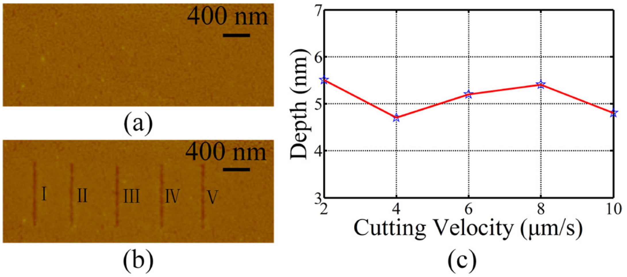
2.2. Choosing the Cutting Force

A separate study was carried out to determine the cutting force required to machine the assembled graphene. Preferably, the cutting force should be high enough to cut through the graphene while having a minimal impact on the substrate underneath. In the study, the graphene is machined by an AFM-based mechanical cutting method using a custom-designed manipulation software. The cutting tool is a diamond-coating AFM tip (DDESP-10) with a tip radius of 35 nm.
In the graphene cutting process, the normal forces (FN) imposed on the graphene can be determined by:
F N = c N S Z V N
where c N is the calibrated normal spring constant of the AFM tip (42 N/m), S Z is the PSD sensitivity (54 nm/V) obtained from the force curve, and V N is the vertical deflection signal of the position-sensitive detector (PSD). F N is adjusted by changing V N .
The relationship between the cutting depth and the normal force is derived as followed. The relationship between A H and F N is evaluated as:
F N = p A H
where p is the yield average pressure of fabricated materials in the vertical direction and A H is the horizontal projected area of the interface between the AFM tip and the surface. The horizontal projected area can be determined by:
A H π R D
where D is the cutting depth and R is the radius of the AFM tip. Combining Equation (3) and Equation (2) yields:
D = k F N
where k = 1 / π R p .
From Equation (4), it can be concluded that the cutting depth is linearly proportional to the normal force. An experimental study is carried out to verify this linear relationship.
The graphene sample is assembled onto a microchip, and the thickness of the graphene is measured to be about 4.3 nm, as shown in Figure 2. The reason the overall graphene thickness is larger than a pure graphene monolayer is due to residual polymethyl methacrylate (PMMA) in the assembly process of the graphene [18]. The graphene is cut at various V N of 6, 7, 8, and 9 V at the same cutting velocity of 2 μm/s. F N at V N of 6, 7, 8, and 9 V are 13.6, 15.88, 18.14, and 20.4 μN, respectively. Figure 3 demonstrates the experimental result. Figure 3c indicates the relationship between the cutting depth and the normal force is indeed linear. Based on the thickness of the graphene sample and this linear relationship, the appropriate cutting force for machining graphene can be determined. For example, when the normal force is 15.88 μN, the cutting depth is 4.9 nm, as shown in Figure 3c. At this cutting depth, the 4.3 nm thick graphene sample shown in Figure 2a is cut through. There is a minimal impact on the 300 nm thick SiO2 dielectric layer, which is used in subsequent experiments. Figure 4 demonstrates the effect of the cutting velocity. Different cutting velocities of 2, 4, 6, 8, and 10 μm/s with a fixed normal force of 15.88 μN are investigated. No specific relationship is observed between the cutting depth and the cutting velocity, as shown in Figure 4c. For the subsequent experiments, the cutting velocity was selected according to the length of the graphene to be machined.
Figure 2. (a) Height image of the graphene in AFM tapping mode and (b) height analysis trace along the white line in (a).
Micromachines 06 01317 g002
Figure 3. (a) Height image of the graphene before cutting; (b) height image of the graphene after cutting at different normal forces of 13.6 μN (I), 15.88 μN (II), 18.14 μN (III), and 20.4 μN (IV) with a cutting velocity of 2 μm/s; and (c) the cut depth versus the normal force.
Micromachines 06 01317 g003
Figure 4. (a) Height image of the graphene before cutting; (b) height image of the graphene after cutting at cutting velocities of 2 μm/s (I), 4 μm/s (II), 6 μm/s (III), 8 μm/s (IV), and 10 μm/s (V) with normal force of 15.88 μN; and (c) the cut depth versus the cutting velocity.
Micromachines 06 01317 g004

2.3. Designing the Cutting Path

A cutting path of the AFM tip is designed to convert the continuous graphene into interdigitated electrodes. The hexagonal graphene assembled on the gold electrodes is shown in Figure 5a. The cutting path shown in Figure 5b consists of the following two steps: (1) the graphene on both sides of the Au electrodes is first cut through to reduce the width of the grapheme; (2) the resulting graphene ribbon is then cut along a zigzag path to achieve the interdigitated electrodes, as shown in Figure 5c.
Figure 5. The cutting path design. (a) Graphene assembled on microelectrodes; (b) sequence of cutting paths; and (c) structure of the graphene interdigitated electrodes.
Micromachines 06 01317 g005

2.4. Effects of Defects on the Electrical Properties of Graphene

As an electrode material, graphene consists of fabrication-induced structural defects that can significantly affect its electronic properties and the performance of graphene-based devices. Therefore, a thorough study of the defects in graphene is critically important before the fabrication of the graphene electrodes. Direct observation of the topological defects in graphene is quite rare [19,20]. In these studies, the location of the induced defect is not well controlled, and complicated experimental methods are needed. There is a need to develop a reliable methodology through which graphene defects can be induced in a controlled manner and examined at the same time. In this study, an AFM-based mechanical cutting method is developed to induce graphene defects at specific locations and analyze these defects at the same time.
Figure 6 shows the formation and analysis of line defects in graphene. An AFM image of the pristine graphene before defect induction is shown in Figure 6a. The I-V curve of this graphene is shown in Figure 6b. In order to better evaluate the effect of defects, we first cut the graphene into a 2 μm ribbon, as shown in Figure 6c. Defects in the form of a single scratch, and then two line scratches, are induced in the graphene ribbon, as shown in Figure 6e,g. The electrical resistance of the graphene samples shown in Figure 6b,d,f,h are 0.51, 1.39, 1.63, and 2.22 kΩ, respectively. Based on these measurements, it can be concluded that a graphene ribbon with line defects exhibits electrical degradation. The fabrication-induced structural defects in the graphene give rise to lattice disturbance which can affect the electronic properties of the graphene due to Anderson localization [21], which is consistent with the theoretical prediction of the influence of defects on the electrical properties of graphene.
Figure 6. Electrical characterization of graphene with and without line defects. (a) AFM image of graphene before defects are induced; (b) I-V curve before defects are induced; (c) AFM image of 2 μm wide graphene ribbon; (d) I-V curve of 2 μm wide graphene ribbon. (e) AFM image of graphene after first defect is induced in the graphene ribbon. The red ellipse indicates the location of the defect; (f) I-V curve after first defect is induced in the graphene ribbon; (g) AFM image of graphene after second defect is induced; and (h) I-V curve after second defect is induced.
Micromachines 06 01317 g006

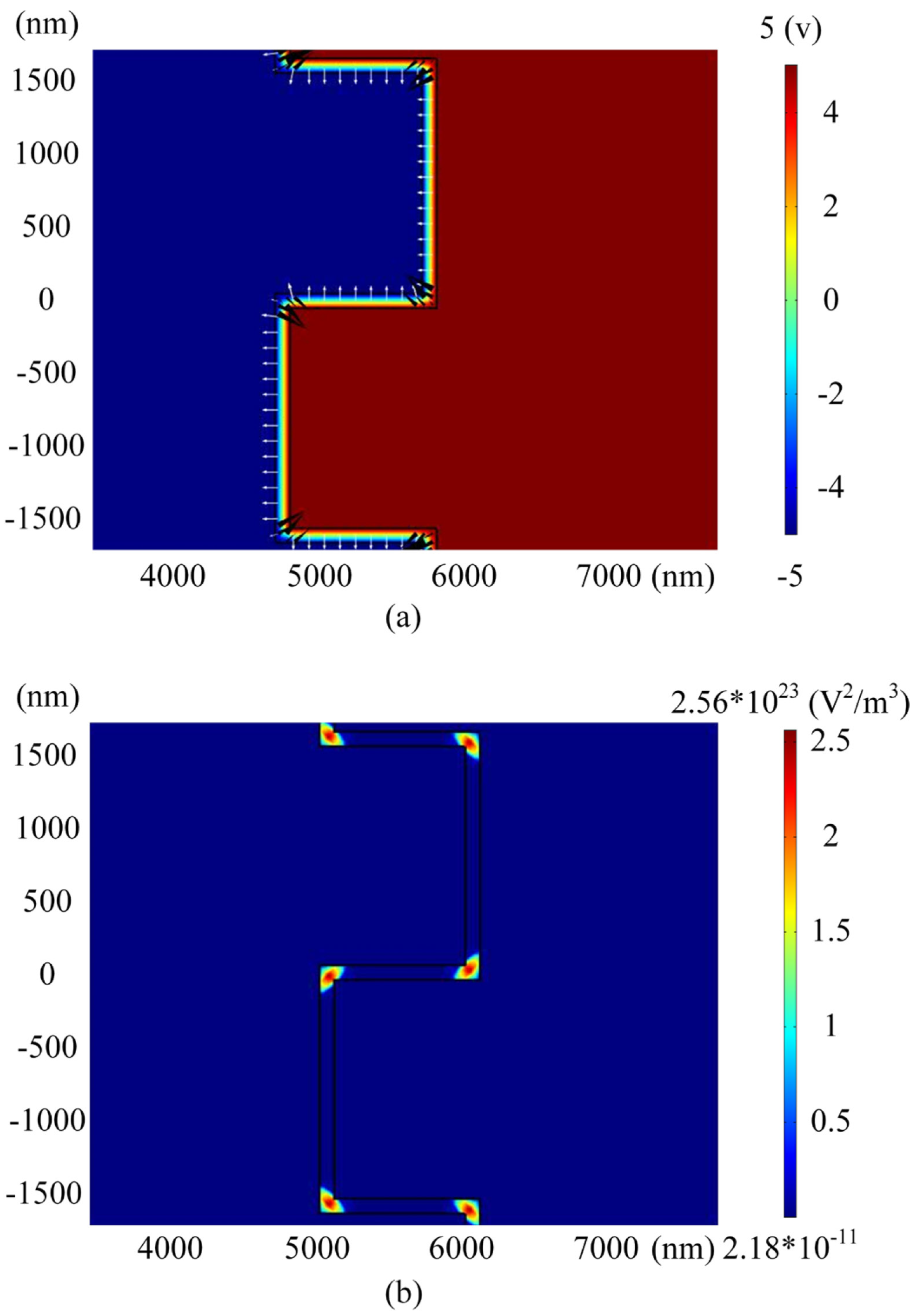
2.5. SWCNT Suspension Preparation and Dielectrophoretic Assembly

High-quality SWCNT suspension is prepared for assembling SWCNTs on graphene electrodes. The dispersion and purification methods of the suspension have been described in our previous publication [22].
Dielectrophoresis [23] has been employed in many electric field-driven alignment processes. In the present study, an alternating current (AC) voltage is applied to the graphene interdigitated electrodes to generate a homogenous electric field in the electrode gap. When a drop of the SWCNT suspension is deposited in the gap, differences in the dielectric permittivity of the SWCNTs and the surrounding medium give rise to a dielectrophoretic force that moves and aligns the deposited SWCNTs following the electric field direction between the electrodes.

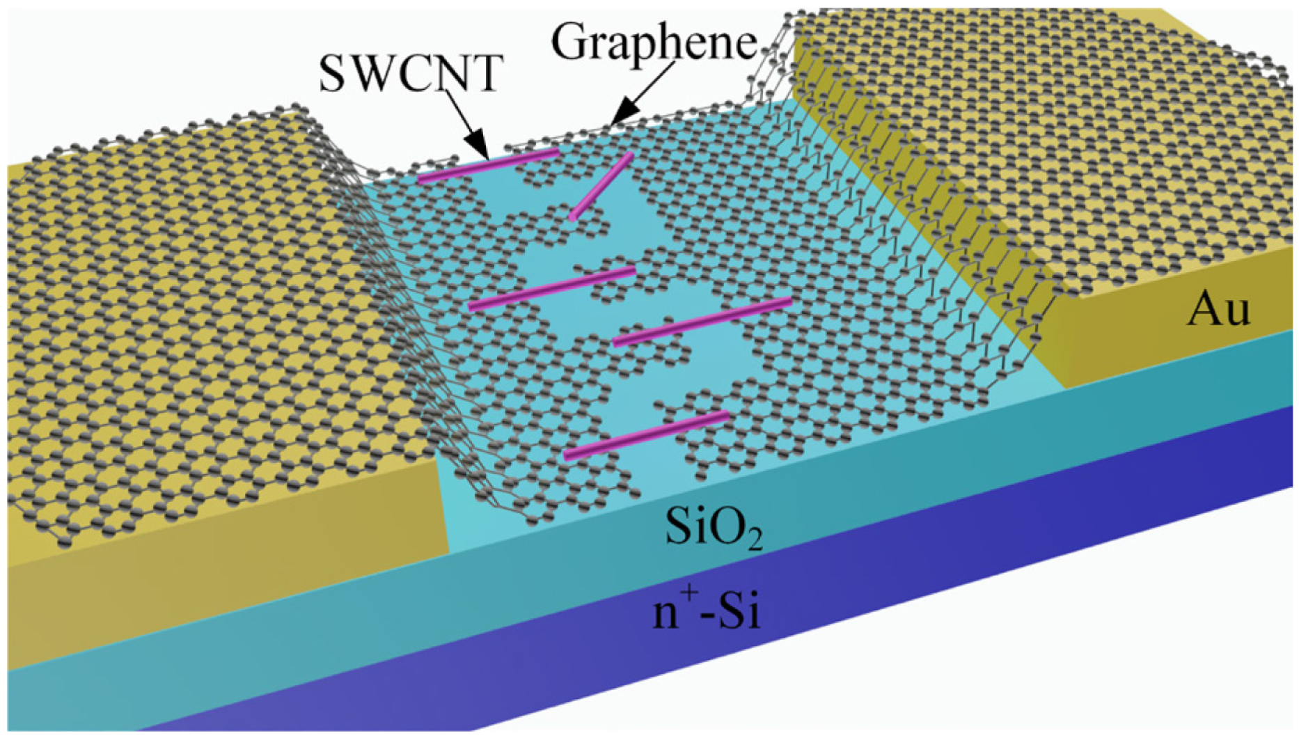
3. Fabrication and Characterization of SWCNT-Graphene FET

The fabrication process of the SWCNT-graphene FET is as follows: graphene is first assembled on a silicon chip with a 300-nm thick SiO2 as the dielectric layer and an n-doped Si substrate as the gate. Next, the AFM-based mechanical cutting method is used to cut the graphene into interdigitated electrodes. They serve as the source and drain of the FET. Finally, SWCNTs are assembled on the graphene interdigitated electrodes by dielectrophoresis to form the conductive channel. The schematic of SWCNT-graphene FET is shown in Figure 7.
Figure 7. Schematic of the SWCNT-graphene FET.
Micromachines 06 01317 g007

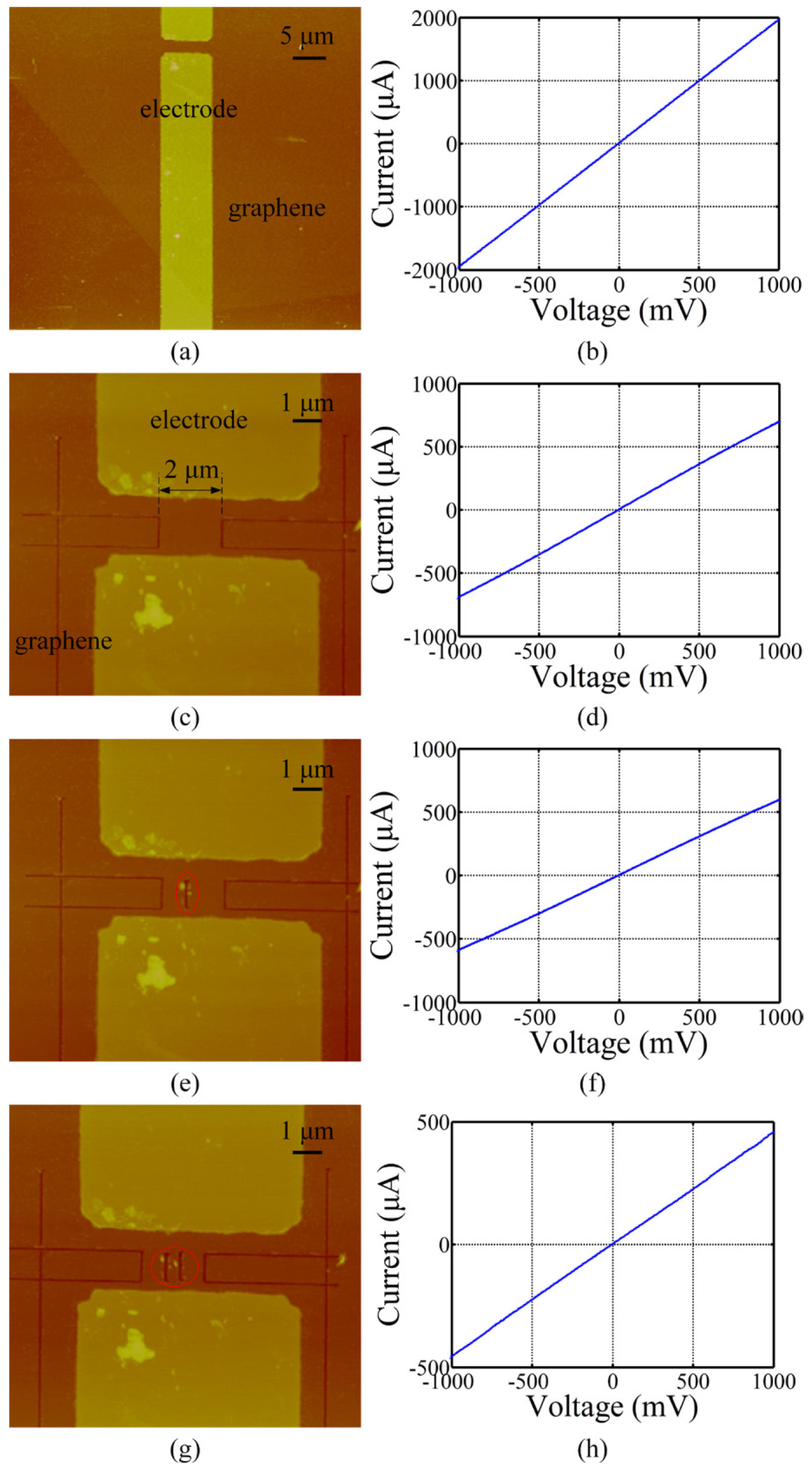
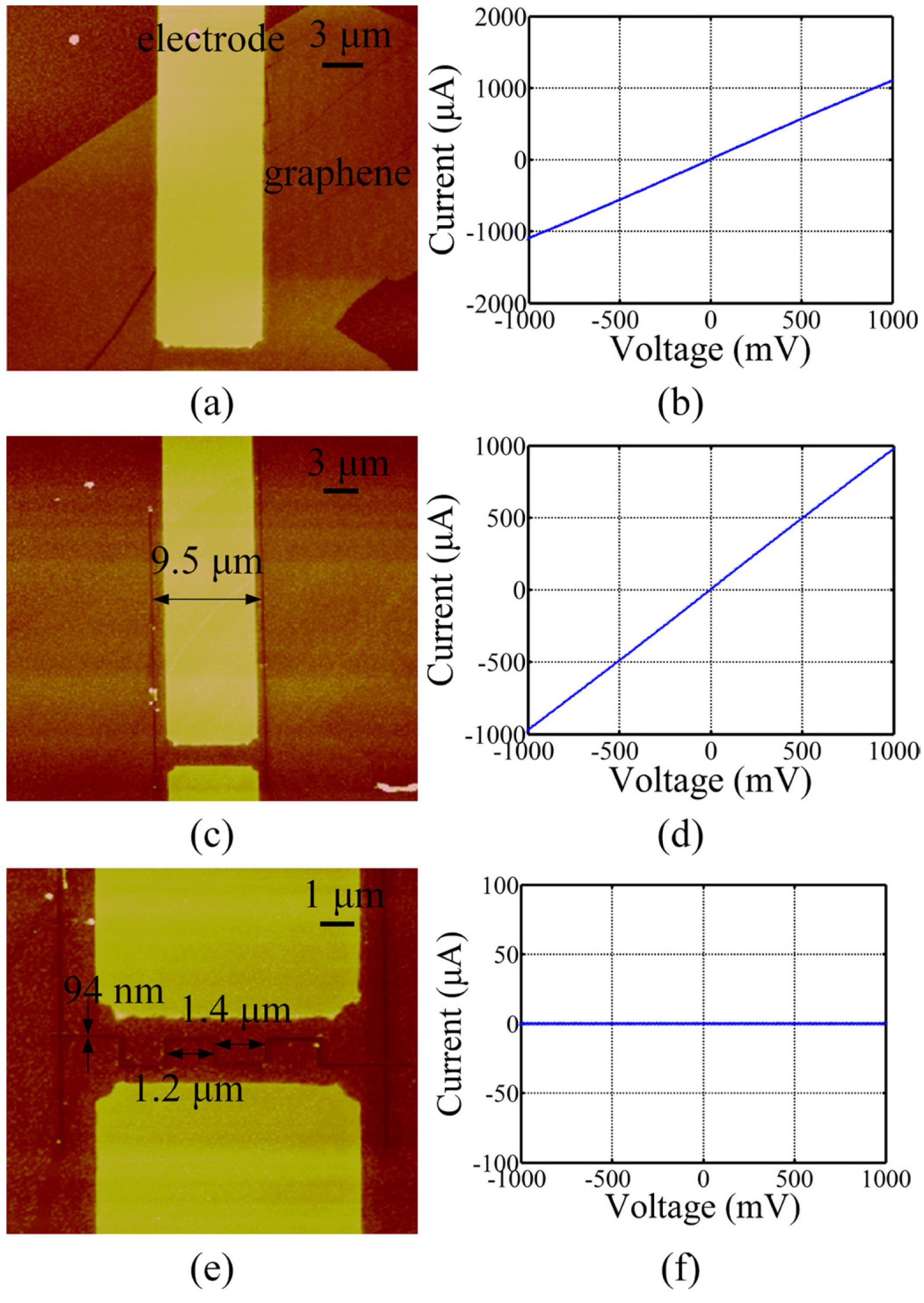
3.1. Characterization of Graphene Interdigitated Electrodes

The I-V curve of the pristine graphene assembled on the microchip as shown in Figure 8a is shown in Figure 8b. The source voltage ranges from −1 to 1 V at 10 mV steps. It can be observed that the I-V curve is linear. The electrical resistance is about 0.88 kΩ, which represents a combination of the electrical resistance of the following components: graphene, Au electrodes, the contact between graphene and Au electrodes, and the contact between Au electrodes and the conductive tip used for the measurement. Figure 8c demonstrates a graphene ribbon with a width of 9.5 μm, fabricated according to the cutting step 1 in Figure 5b. Its I-V curve is shown in Figure 8d. It can be seen that the I-V curve is linear as well. The corresponding electrical resistance of the ribbon is about 1 kΩ, which is higher than that of the pristine graphene shown in Figure 8a. This result verifies that when the width of a graphene sample decreases, its resistance increases.
The graphene ribbon is cut through along a zigzag path into two interdigitated electrodes, as displayed in Figure 8e. Figure 8f demonstrates the absence of current flow between the graphene electrodes, proving that the graphene ribbon is cut through completely. The smallest nanogap width between the graphene interdigitated electrodes is 94 nm. The average width is 97 nm and the standard deviation (SD) is 3.6 nm. The widths of the smallest and largest electrode fingers are 1.1 μm and 1.8 μm, respectively. The graphene interdigitated electrodes with a nanogap can be used to characterize the electrical properties of any nanoscale material placed in the nanogap.
Figure 8. Height image of the graphene ribbon. (a) AFM image before cutting; (b) I-V curve before cutting; (c) AFM image after the first cut. The width of the graphene ribbon between the electrodes is 9.5 μm; (d) I-V curve after the first cut; (e) AFM image after interdigitated electrodes are formed; and (f) I-V curve after interdigitated electrodes are formed.
Micromachines 06 01317 g008

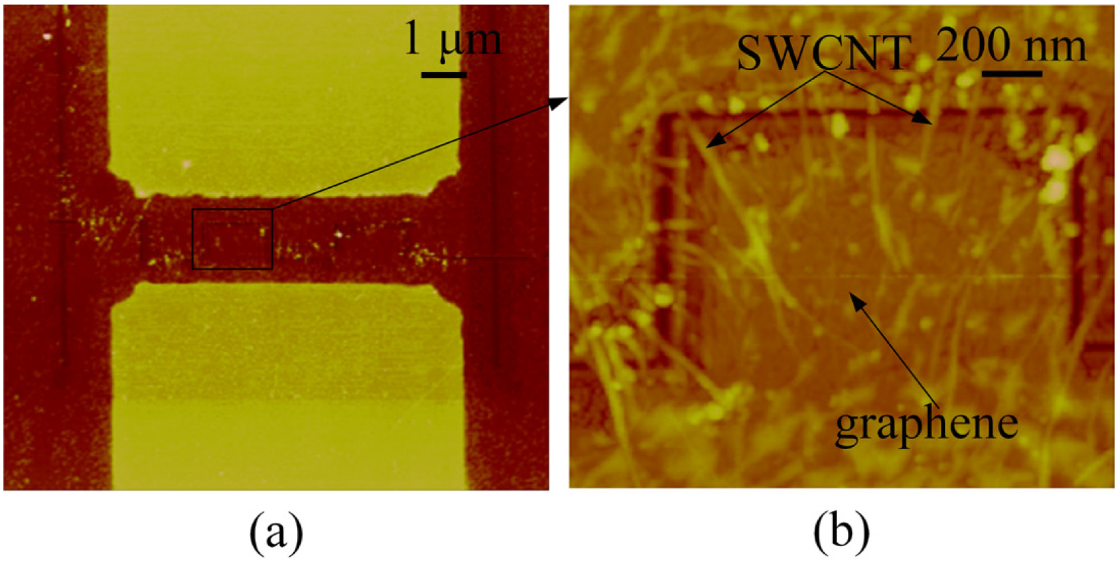
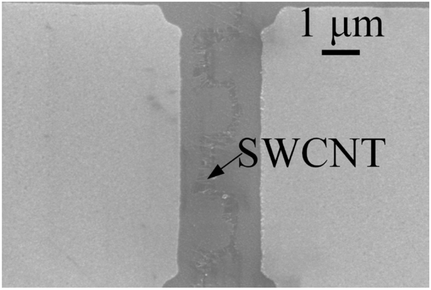
3.2. Assembly of SWCNT on Graphene Interdigitated Electrodes by Dielectrophoresis

After the fabrication of the graphene interdigitated electrodes, SWCNTs are assembled onto the electrodes by dielectrophoresis to form a conductive channel. If the external electric field used in the dielectrophoresis process is nonhomogenous, the SWCNTs will experience a dielectrophoretic force, as defined by the following equation [24]:
F = π r 2 l ε m R e [ f c m ] E r m s 2 / 6
where r is the radius of the SWCNTs, l is the length the SWCNTs, R e [ f c m ] is the real part of the Clausius-Mossotti factor f c m , and E r m s is the gradient of the root mean square value of the external electric field. The Clausius-Mossotti factor f c m can be determined by:
f c m = ( ε p * ε m * ) / ( ( ε p * ε m * ) A L + ε m * )
ε * = ε j σ / ω
where ε * is the complex permittivity that consists of the physical permittivity ε, conductivity σ, and the angular velocity ω of the external electric field. The subscripts p and m represent the particle and the medium, respectively. A L is the depolarization factor along the long axis.
For SWCNT, the dielectrophoretic force is determined by the real part of the Clausius-Mossotti factor f c m and E r m s 2 . R e [ f c m ] mainly contributes to the magnitude of the dielectrophoretic force while E r m s 2 determines both the magnitude and the direction of the dielectrophoretic force. Once the particle, medium, and angular velocity of the external electric field are defined, the dielectrophoretic force is proportional to E r m s 2 as described in Equation (5).
To better understand the assembly process of SWCNTs between the graphene interdigitated electrodes described above, the electric field and E r m s 2 distribution generated by the electrodes is simulated by COMSOL Multiphysics coupling software. Figure 9a shows the potential and direction of the electric field and E r m s 2 distribution. The white arrows indicate the direction of the electric field. The black arrows indicate the direction of E r m s 2 , which mainly point towards the corner of the graphene interdigitated electrode gap according to the simulation. This result implies that the direction of the dielectrophoretic force points towards the corners of the graphene interdigitated electrode gap. Figure 9b shows the contour map of the E r m s 2 magnitude. It can be seen that E r m s 2 is mainly concentrated in the corners of the electrode gap, and the largest dielectrophoretic force experienced by the SWCNTs is therefore also at the corners of the electrode gap according to the simulation.
In the assembly process of SWCNTs by dielectrophoresis, control parameters, such as the alignment voltage, frequency, and duration, must be closely regulated and monitored. Accordingly, an electrophoresis assembly system is developed to carry out the assembly process. In this process, one 2 μL drop of diluted SWCNT solution is placed on the graphene electrode chip using a pipette. Then an AC voltage is applied to the graphene electrodes at a frequency of 1 MHz and peak-to-peak voltage of 10 V by an arbitrary function generator (Escort, Taipei, Taiwan) to generate a dielectrophoretic force to assemble and align the SWCNTs in the graphene interdigitated electrodes gap. After 3–5 s, the AC voltage is switched off. The actual number of SWCNTs assembled in the nanogap is affected by the time the AC voltage is applied. After alignment, the electrode chip is tilted at 45° angle and slowly rinsed by deionized water for about 50 s to move the remains of sodium dodecyl sulfate. Then, the chip dried at room temperature.
The completed SWCNT-graphene FET is shown in Figure 10. From Figure 10a, it can be seen that all SWCNTs are distributed between the graphene interdigitated electrodes. The diameter of the SWCNT is about 2.5 nm, and the length of the SWCNT is from 180 nm to 1.2 μm, as shown in Figure 10b. It can be seen that the SWCNTs are mostly distributed around the corners of the graphene electrodes, and the experimental and simulation results agree well. In order to prove that the SWCNTs are constrained to the nanogaps and not extended all the way to Au electrodes, the SEM image of the area between the Au electrodes is shown in Figure 11. In this all-carbon FET fabricated by assembled SWCNTs on graphene interdigitated electrodes, the only pathway for charge transport is through the junctions between the graphene and SWCNTs. The SWCNTs do not have any physical connection with the Au electrodes, and the Au electrodes are only used to form electrical connections with the external electronics for measurement.
Figure 9. Numerical simulation of potential, electric field, and E r m s 2 distribution generated by an external AC voltage. (a) Potential and direction of electric field and E r m s 2 distribution and (b) E r m s 2 magnitude distribution.
Micromachines 06 01317 g009
Figure 10. (a) AFM image of SWCNT-graphene FET and (b) partial enlargement figure of (a).
Micromachines 06 01317 g010
Figure 11. SEM image of SWCNT-graphene FET.
Micromachines 06 01317 g011

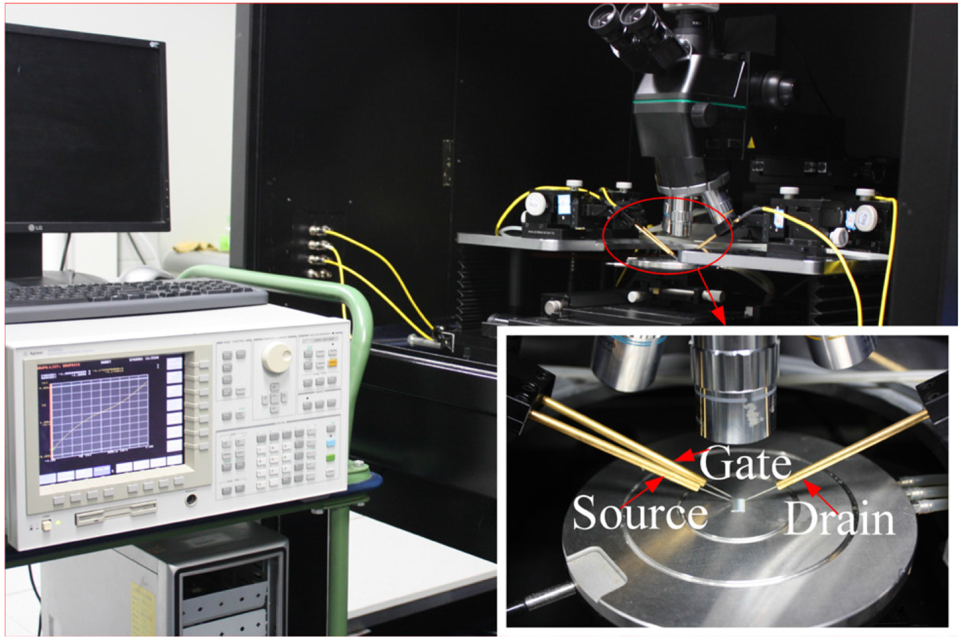
3.3. SWCNT-Graphene FETs Characteristic Test

The electrical characteristics of the SWCNT-graphene FET are investigated after the assembly. The FET characterization system is built as shown in Figure 12. Three metal needle probes serve as the electrical contacts to the FET. The I-V curves are collected by an Agilent 4155C semiconductor parameter analyzer (Agilent, Tokyo, Japan). Figure 13 shows the characterization results of the SWCNT-graphene FET at room temperature. The gate voltage varies from −16 to 16 V, and the source-drain voltage varies from −1 to 1 V at 10 mV steps. The source-drain current decreases gradually as the gate voltage is raised from −16 to +16 V, demonstrating an effective physical assembly and electrical connection between the SWCNTs and graphene, and indicating a p-type behavior in the device channel. When the source-drain voltage is −1 V, and the gate voltage is +16 V, the source-drain current is lower than −1000 nA. When the gate voltage is −16 V, the source-drain current is about −2535 nA at a source-drain voltage of −1 V. The low on-off ratio in this device indicates the presence of metallic SWNTs in the conductive channel, which are not modulated by the gate voltage. It is noted that the performance of the FET could be potentially improved by an electrical burning process to remove the metallic SWCNTs [25]. The structure of the graphene electrodes and length of the conductive channel can be changed by selecting the appropriate AFM tip and designing different cutting paths, which can then be used to investigate the variation of I-V curves and further improve the quality of the FET.
Figure 12. SWCNT-graphene FET electrical characterization system.
Micromachines 06 01317 g012
Figure 13. SWCNT-graphene FET electrical characteristics.
Micromachines 06 01317 g013

4. Conclusions

In this paper, graphene grown by CVD is assembled onto a Au microelectrode chip through the bubbling method. An AFM-based mechanical cutting method is then used to cut the assembled graphene first into a ribbon, and then into interdigitated electrodes with a nanogap. The electrical properties of the graphene ribbon are measured after each cut. As the width of the ribbon decreases, the resistance increases. The width of the nanogap between the graphene interdigitated electrodes is 94 nm. The widths of the smallest and largest electrode are 1.1 μm and 1.8 μm, respectively. The graphene interdigitated electrodes with a nanogap have the potential to be used to probe macromolecules in the one hundred nanometers range [26]. By selecting the appropriate AFM tip, cutting force, and number of cutting passes, the width of the graphene electrodes and nanogap can be further reduced to increase the density of the electrodes and increase the sensitivity and response time of a molecular sensor based on the graphene electrodes. On this basis, SWCNTs are assembled onto graphene interdigitated electrodes using dielectrophoresis for the first time. The SWCNTs are concentrated around the corners of the interdigitated electrodes, as predicted by numerical simulation. Preliminary verification indicates the SWCNT-graphene FET exhibits p-type behavior, which presents a new approach to build all-carbon electronic devices.

Acknowledgments

This research work was partially supported by the National Natural Science Foundation of China (Grant Nos. 61573339, 61304251 and 61503258), and the CAS FEA International Partnership Program for Creative Research Teams.

Author Contributions

Shuangxi Xie, Niandong Jiao and Lianqing Liu proposed the idea; Shuangxi Xie and Niandong Jiao performed the research; Shuangxi Xie, Niandong Jiao and Steve Tung prepared the manuscript; Steve Tung and Lianqing Liu gave valuable suggestions on the manuscript revision.

Conflicts of Interest

The authors declare no conflicts of interest.

References

  1. Geim, A.K.; Novoselov, K.S. The rise of graphene. Nat. Mater. 2007, 6, 183–191. [Google Scholar] [CrossRef] [PubMed]
  2. Eda, G.; Chhowalla, M. Graphene-based composite thin films for electronics. Nano Lett. 2009, 9, 814–818. [Google Scholar] [CrossRef] [PubMed]
  3. Geim, A.K. Graphene: Status and prospects. Science 2009, 324, 1530–1534. [Google Scholar] [CrossRef] [PubMed]
  4. Lee, C.; Wei, X.; Kysar, J.W.; Hone, J. Measurement of the elastic properties and intrinsic strength of monolayer graphene. Science 2008, 321, 385–388. [Google Scholar] [CrossRef] [PubMed]
  5. Li, X.; Wang, X.; Zhang, L.; Lee, S.; Dai, H. Chemically derived, ultrasmooth graphene nanoribbon semiconductors. Science 2008, 319, 1229–1232. [Google Scholar] [CrossRef] [PubMed]
  6. Wu, Y.; Lin, Y.; Bol, A.A.; Jenkins, K.A.; Xia, F.; Farmer, D.B.; Zhu, Y.; Avouris, P. High-frequency, scaled graphene transistors on diamond-like carbon. Nature 2011, 472, 74–78. [Google Scholar] [CrossRef] [PubMed]
  7. Yang, X.; Cheng, C.; Wang, Y.; Qiu, L.; Li, D. Liquid-mediated dense integration of graphene materials for compact capacitive energy storage. Science 2013, 341, 534–537. [Google Scholar] [CrossRef] [PubMed]
  8. Schedin, F.; Geim, A.K.; Morozov, S.V.; Hill, E.W.; Blake, P.; Katsnelson, M.I.; Novoselov, K.S. Detection of individual gas molecules adsorbed on graphene. Nat. Mater. 2007, 6, 652–655. [Google Scholar] [CrossRef] [PubMed]
  9. Li, B.; Cao, X.; Ong, H.G.; Cheah, J.W.; Zhou, X.; Yin, Z.; Li, H.; Wang, J.; Boey, F.; Huang, W.; et al. All-Carbon Electronic Devices Fabricated by Directly Grown Single-Walled Carbon Nanotubes on Reduced Graphene Oxide Electrodes. Adv. Mater. 2010, 22, 3058–3061. [Google Scholar] [CrossRef] [PubMed]
  10. Hong, S.W.; Du, F.; Lan, W.; Kim, S.; Kim, H.; Rogers, J.A. Monolithic Integration of Arrays of Single-Walled Carbon Nanotubes and Sheets of Graphene. Adv. Mater. 2011, 23, 3821–3826. [Google Scholar] [CrossRef]
  11. Zou, Y.; Li, Q.; Liu, J.; Jin, Y.; Qian, Q.; Jiang, K.; Fan, S. Fabrication of All-Carbon Nanotube Electronic Devices on Flexible Substrates Through CVD and Transfer Methods. Adv. Mater. 2013, 25, 6050–6056. [Google Scholar] [CrossRef]
  12. Avouris, P.; Chen, Z.; Perebeinos, V. Carbon-based electronics. Nat. Nanotechnol. 2007, 2, 605–615. [Google Scholar] [CrossRef]
  13. Shiraishi, M.; Ata, M. Work function of carbon nanotubes. Carbon 2001, 39, 1913–1917. [Google Scholar] [CrossRef]
  14. Liu, P.; Sun, Q.; Zhu, F.; Liu, K.; Jang, K.; Liu, L.; Li, Q.; Fan, S. Measuring the work function of carbon nanotubes with thermionic method. Nano Lett. 2008, 8, 647–651. [Google Scholar] [CrossRef] [PubMed]
  15. Tongay, S.; Lemaitre, M.; Miao, X.; Gila, B.; Appleton, B.R.; Hebard, A.F. Rectification at graphene-semiconductor interfaces: Zero-gap semiconductor-based diodes. Phys. Rev. X 2012, 2, 011002. [Google Scholar] [CrossRef]
  16. Zeng, J.J.; Lin, Y.J. Tuning the work function of graphene by nitrogen plasma treatment with different radio-frequency powers. Appl. Phys. Lett. 2014, 104, 233103. [Google Scholar] [CrossRef]
  17. Cao, Q.; Hur, S.H.; Zhu, Z.T.; Sun, Y.; Wang, C.; Meitl, M.A.; Shim, M.; Rogers, J.A. Highly Bendable, Transparent Thin-Film Transistors That Use Carbon-Nanotube-Based Conductors and Semiconductors with Elastomeric Dielectrics. Adv. Mater. 2006, 18, 304–309. [Google Scholar] [CrossRef]
  18. Gao, L.; Ren, W.; Xu, H.; Jin, L.; Wang, Z.; Ma, T.; Ma, L.P.; Zhang, Z.; Fu, Q.; Peng, L.M.; et al. Repeated growth and bubbling transfer of graphene with millimetre-size single-crystal grains using platinum. Nat. Commun. 2012, 3, 699. [Google Scholar] [CrossRef] [PubMed]
  19. Meyer, J.C.; Kisielowski, C.; Erni, R.; Rossell, M.D.; Crommie, M.F.; Zettl, A. Direct imaging of lattice atoms and topological defects in graphene membranes. Nano Lett. 2008, 8, 3582–3586. [Google Scholar] [CrossRef] [PubMed]
  20. Jafri, S.H.M.; Carva, K.; Widenkvist, E.; Blom, T.; Sanyal, B.; Fransson, J.; Eriksson, O.; Jansson, U.; Grennberg, H.; Karis, O.; et al. Conductivity engineering of graphene by defect formation. J. Phys. D Appl. Phys. 2010, 43, 045404. [Google Scholar] [CrossRef]
  21. Anderson, P.W. Absence of diffusion in certain random lattices. Phys. Rev. 1958, 109, 1492–1505. [Google Scholar] [CrossRef]
  22. Xu, K.; Tian, X.J.; Wu, C.D.; Liu, J.; Li, M.X.; Dong, Z.L. Study on the large-scale assembly and fabrication method for SWCNTs nano device. Sci. China Phys. Mech. Astron. 2013, 56, 556–561. [Google Scholar] [CrossRef]
  23. Pohl, H.A. The motion and precipitation of suspensoids in divergent electric fields. J. Appl. Phys. 1951, 22, 869–871. [Google Scholar] [CrossRef]
  24. Dimaki, M.; Bøggild, P. Dielectrophoresis of carbon nanotubes using microelectrodes: A numerical study. Nanotechnology 2004, 15, 1095. [Google Scholar] [CrossRef]
  25. Bartolomeo, A.D.; Rinzan, M.; Boyd, A.K.; Yang, Y.; Guadagno, L.; Giubileo, F.; Barbara, P. Electrical properties and memory effects of field-effect transistors from networks of single-and double-walled carbon nanotubes. Nanotechnology 2010, 21, 115204. [Google Scholar] [CrossRef] [PubMed]
  26. Li, T.; Hu, W.; Zhu, D. Nanogap electrodes. Adv. Mater. 2010, 22, 286–300. [Google Scholar] [CrossRef] [PubMed]

