Article

A Novel Bulk Acoustic Wave Resonator for Filters and Sensors Applications

State Key Laboratory of Precision Measuring Technology and Instruments, Tianjin University, Tianjin 300072, China
*
Author to whom correspondence should be addressed.
Micromachines 2015, 6(9), 1306-1316; https://doi.org/10.3390/mi6091306
Submission received: 24 July 2015 / Revised: 20 August 2015 / Accepted: 1 September 2015 / Published: 8 September 2015
(This article belongs to the Special Issue Microresonators)

Abstract

:
Bulk acoustic wave (BAW) resonators are widely applied in filters and gravimetric sensors for physical or biochemical sensing. In this work, a new architecture of BAW resonator is demonstrated, which introduces a pair of reflection layers onto the top of a thin film bulk acoustic resonator (FBAR) device. The new device can be transformed between type I and type II dispersions by varying the thicknesses of the reflection layers. A computational modeling is developed to fully investigate the acoustic waves and the dispersion types of the device theoretically. The novel structure makes it feasible to fabricate both type resonators in one filter, which offers an effective alternative to improve the pass band flatness in the filter. Additionally, this new device exhibits a high quality factor (Q) in the liquid, which opens a possibility for real time measurement in solutions with a superior limitation of detection (LOD) in sensor applications.

1. Introduction

Bulk acoustic wave (BAW) resonators based on aluminum nitride (AlN) are one of the success stories in modern microwave technologies. AlN based BAW resonators have two basic architectures: Thin Film Bulk Acoustic Wave Resonator (FBAR), which is suspended above an air cavity, and Solidly Mounted Resonator (SMR), which utilizes a series of high and low impedance reflectors to isolate the resonator from the substrate. Thanks to their miniature sizes, high quality factors (Q) in air, and compatibilities with integrated circuit processing, BAW resonators have been used in a widespread applications, such as filters and duplexers in communication electronics [1,2], oscillators for frequency control, gravimetric sensors for physical [3], chemical [4] and biological [5,6] sensing, and general physics applications [7].
For filter and duplexer applications, the spurious modes in resonators inevitably induce ripples in the pass band, which greatly degrade the flatness. Enlarging the resonator area in the series branch of the filter can subdue the ripples in the pass band, whereas it lowers the out-of-band rejection at a price. Though the flatness in the pass band can also be improved by introducing a frame or other structures into the device [8], the introduced structures need to be optimized in several processing cycles, which complicates the device fabrication. An alternative method to improve the pass band flatness of the filter is to deploy dispersion type I and type II resonators for series and shunt branches, respectively, in a filter. Since the locations of spurious modes in frequencies are different according to the different dispersion types of resonators, the ripples in the pass band can be moved to the edge, which contributes to the pass band flatness significantly. However, AlN FBARs exhibit fixed dispersion type II properties, failing to be applied for this method. Though the acoustic dispersion type of an SMR can be tailored by tuning the thickness of the reflection layers [9,10], it is difficult to fabricate both type devices on the same chip, since the reflectors are at the bottom of the device.
In this paper, we present a new BAW resonator device, in which a reflection stack with specific thicknesses is introduced onto the top of an FBAR. Though the dependence of dispersion types on the stack was investigated before [9,11], the quantitative relations between them are not clarified yet. In this paper, we theoretically analyze the device stack through the computational modeling. As a result, the dispersion type of a given stack can be predicted. By varying the thicknesses of the reflection layers, the acoustic dispersion type of the device can be tailored. Since the reflection layers are on the top of the device, the dispersion relations could be post-tuned when the fabrication is accomplished, and it is also possible in process to fabricate resonators with both type I and type II dispersion types on one chip.
In addition, for sensing applications, the quality factor (Q) is a key parameter to guarantee the limitation of detection (LOD) of sensors. Since most biochemical sensing experiments are conducted in liquids, and real time measurements of frequency shifts are desirable, it is in great demand for resonators with high Q values in the liquid environment. Although the Q factors of FBAR and SMR devices are extremely high in air, they decline sharply when immerging in a liquid [12,13]. Therefore, it is desirable to develop devices with high Q factors in liquids. In this work, as the reflector layers are on the top of the device, they can serve as an isolator to attenuate the acoustic wave leakage when the device is immerged in the liquid, preserving a high Q factor of the resonator.

2. Experimental Section

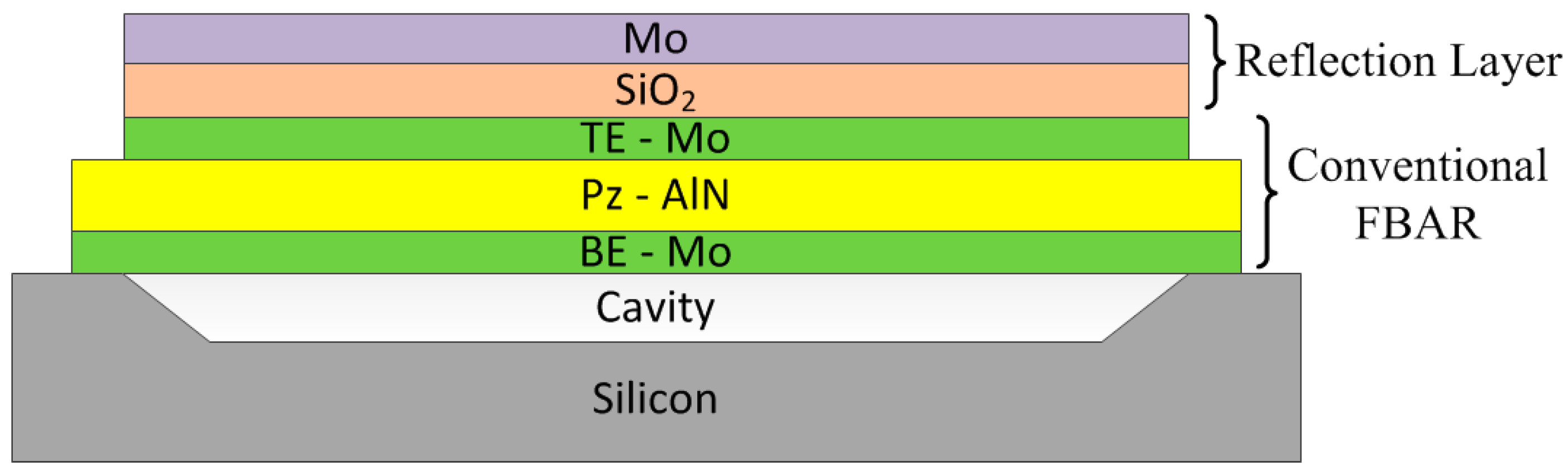
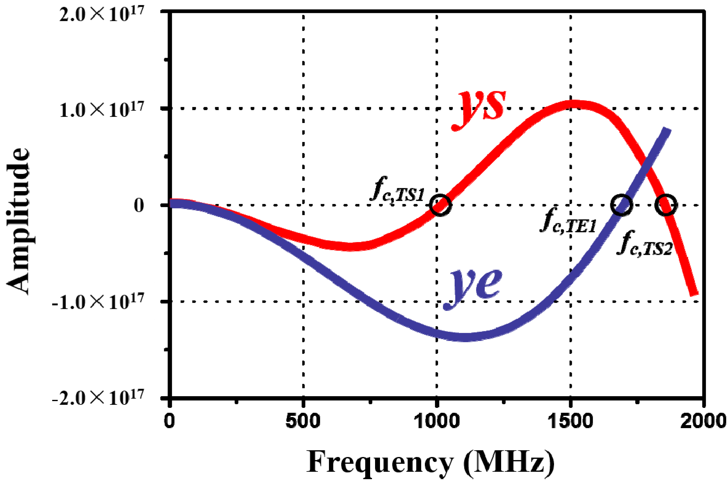
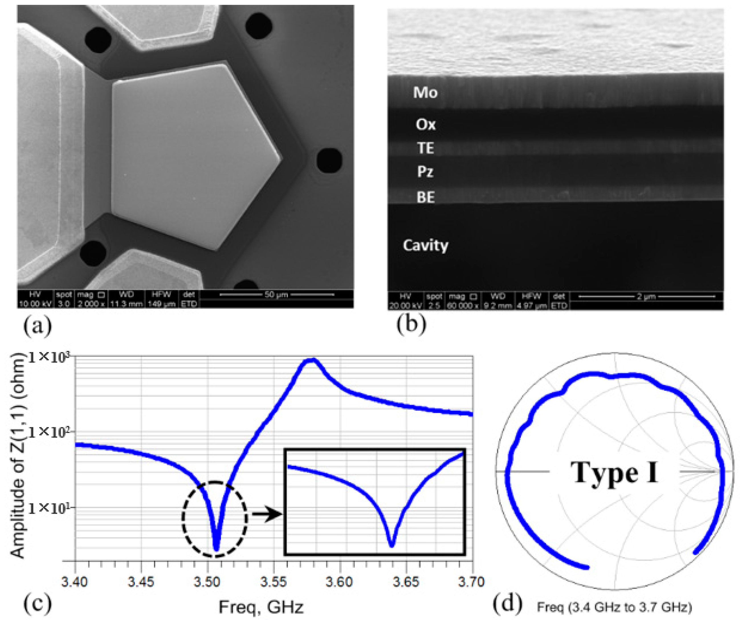
2.1. Device Architecture and Computational Modeling

The device is consisted of a conventional FBAR, which includes a piezoelectric layer sandwiched by top and bottom electrodes, and a reflection stack from the bottom up, as depicted in Figure 1. The reflection stack is composed of a silicon oxide (SiO2) layer and a molybdenum (Mo) layer. In a BAW resonator, there exist two wave modes—thickness extensional (TE) mode and thickness shear (TS) mode. If the longitudinal cutoff frequency (fc,TE1) (or series resonant frequency fs) is lower than the second shear wave cutoff frequency (fc,TS2), the device is defined as a type II dispersion device. On the contrary, devices whose fc,TE1 is higher than fc,TS2 are type I dispersion devices [8].
Figure 1. Illustration of the cross section of the new device: It is composed of a bottom electrode (BE), piezoelectric layer (Pz), top electrode (TE), and reflection layers.
Micromachines 06 01306 g001
The acoustic dispersion types are susceptible to the stack, and both fc,TE1 and fc,TS2 can be figured out through a Transfer Matrix method [14]. For each layer in the stack, the relations between the field quantities of interest on both surfaces can be described by matrix:
( u v σ τ ) b o t = M i ( u v σ τ ) t o p
where u, v, σ, and τ are the normal displacement, the tangential displacement, the normal stress, and the tangential stress, respectively; the subscripts top and bot represent the top and the bottom surface, respectively; and Mi is the Transfer Matrix of the ith layer. Take the bottom electrode as an example, its Transfer Matrix is:
( cos ( ρ / c 44 t ω ) 0 0 sin ( ρ / c 44 t ω ) ω ρ c 44 0 cos ( ρ / c 11 t ω ) sin ( ρ / c 11 t ω ) ω ρ c 11 0 0 ω ρ c 11 sin ( ρ / c 11 t ω ) cos ( ρ / c 11 t ω ) 0 ω ρ c 44 sin ( ρ / c 44 t ω ) 0 0 cos ( ρ / c 44 t ω ) )
where ω, ρ, c, and t are the frequency, the density, the stiffness, and the thickness, respectively. According to the continuity conditions at the interfaces, the Transfer Matrix of the whole stack can be deduced as follows:
( u v σ τ ) l a s t = M n M n 1 M 2 M 1 ( u v σ τ ) f i r s t = M ( u v σ τ ) f i r s t
where M is a 4 × 4 Transfer Matrix, which condenses a multilayered system into a set of four equations correlating the boundary conditions at the first interface to that at the last interface.
Since both upper and lower surfaces of the device are exposed to air, the stresses on them are zero. Hence, the determination of the 2 × 2 bottom left sub-matrix of M is zero. The determination can be rewritten in the form of a product of two factors, which are named as ye and ys, respectively:
y e y s = 0
where ye and ys are related to TE mode and TS mode, respectively. They are the sums of a few sinusoidal functions in terms of the thickness of each layer in the stack (the detailed derivations and the expressions of ye and ys can be found in the supplementary materials). We set each factor to be zero and solve for the frequencies to obtain the cutoff frequencies of each mode. By comparing the values of fc,TE1 and fc,TS2, we could identify which type the device is. Since these two factors are too complex to be solved by analytic method, we plot ye and ys versus frequencies, as shown in Figure 2. Frequencies at zero crossing points are the cutoff frequencies we are looking for in each mode, and the values of cutoff frequencies can be read out on the axis directly. By comparing the values of fc,TE1 and fc,TS2, the dispersion type of the device can be identified clearly.
Figure 2. Plot of ye and ys versus frequencies. The frequencies at zero crossing points are the cutoff frequencies in each mode (ye and ys are unitless).
Micromachines 06 01306 g002
The relations between cutoff frequencies and stack layers are investigated. For computational simplicity, the thickness ratio of both the top and the bottom electrode to the piezoelectric layer is set to be k, and the ratio of the SiO2 layer and the topmost Mo layer to the piezoelectric layer is set to be kOx and kMo, respectively. Since the cutoff frequencies are functions of k, kOx, and kMo, the investigations are conducted first in the condition of a fixed k value, and it is set to be 0.2. Either kOx or kMo is varied in a series of values while keeping the other as a constant, and both fc,TE1 and fc,TS2 are figured out and plotted in Figure 3a,b. It is known from the figures that the reflection layers have greater impact on fc,TS2 than fc,TE1. When the thickness of SiO2 or Mo layer reaches a certain value, fc,TE1 is equal to fc,TS2, and this is defined as the critical condition for the dispersion type conversion. As the thickness of one of the reflection layers exceeds the critical value, fc,TE1 surpasses fc,TS2, which means that the device is transformed from type II to type I. On the other hand, if the thicknesses of the reflection layers are less than the threshold, the device preserves the characteristic of the type II.
The values of kOx and kMo in the critical conditions for FBAR type transfermation (i.e., in the condition of fc,TE1 = fc,TS2) with various k values are calculated and plotted in Figure 3c. Each curve exhbits a negative correlation between kOx and kMo; that is to say, in the critical conditions, the thickness increase of one reflection layer induces the thickness decrease of the other one. By comparing these curves, it is also observed that larger k value corresponds to larger kOx and kMo, suggesting that thicker reflection layers are needed for type conversion in the device with a smaller piezoelectric coupling coefficient (k2t,eff).
Figure 3. (a) Relations between cutoff frequencies and kMo; (b) Relations between cutoff frequencies and kOx; (c) Combinations of kMo and kOx in the critical conditions for type conversion.
Micromachines 06 01306 g003

2.2. Simulations and Fabrications

A 2D finite element method (FEM) and solver software package (COMSOL MULTIPHYSISCS, Stockholm, Sweden) is adopted for simulations. Through the FEM simulations, a series of spatial amplitude distributions over different frequencies are available. Then, a fast Fourier transform (FFT) algorithm is applied to the amplitude dataset, yielding an amplitude distribution over the lateral propagation constant, thus the dispersion curves are obtained [15]. A type I device is designed following the theory, which is built by 2000 Å Mo, 5000 Å AlN, 2000 Å Mo, 5000 Å SiO2, and 5000 Å Mo from the bottom up. The FEM simulation outcome is illustrated in Figure 4a. fc,TE1 is greater than fc,TS2, suggesting it is a type I resonator, which agrees with the theoretical calculations. The dispersion curves of TE1 mode has its real wave numbers higher in frequency than fc,TE1, indicating that the spurious modes are in the frequency range higher than fs in the resonator. A type II device is also designed and simulated, whose stack is the same as that of the type I except that the top reflection layer of Mo is thinned to 1000 Å. The simulated dispersion relations are presented in Figure 4b. fc,TE1 is less than fc,TS2, exhibiting a characteristic of type II. Since real wave numbers are lower than fc,TE1 in TE1 dispersion branch, the spurious modes locate in frequencies below fs.
A CMOS-compatible AlN Micro-electromechanical Systems (MEMS) fabrication process is employed. The process starts by a RF sputtering deposition of 2000 Å Mo, and a plasma etching is used to pattern it as the bottom electrode. Then, 0.5 μm AlN, 2000 Å Mo, 5000 Å SiO2, and 5000 Å Mo are deposited in turn onto the bottom electrode, respectively. Next, the top two reflection layers are patterned by plasma etching all at once. Wet etching is then used to pattern the top electrode. Subsequently, AlN is etched by a combination of plasma etching and potassium hydroxide (KOH) wet etching. After AlN etch, the bottom electrode can be accessed. Gold (Au) is then evaporated and patterned by lift-off process, serving as electrical connections and testing pads. Finally comes the release by trickling xenon difluoride (XeF2) gas into the release holes to etch the silicon beneath the device, forming an air cavity to reflect acoustic waves.
Figure 4. Dispersion Curves of the new device with the topmost Mo layer of (a) 5000 Å and (b) 1000 Å simulated by a 2D finite element method (FEM).
Micromachines 06 01306 g004

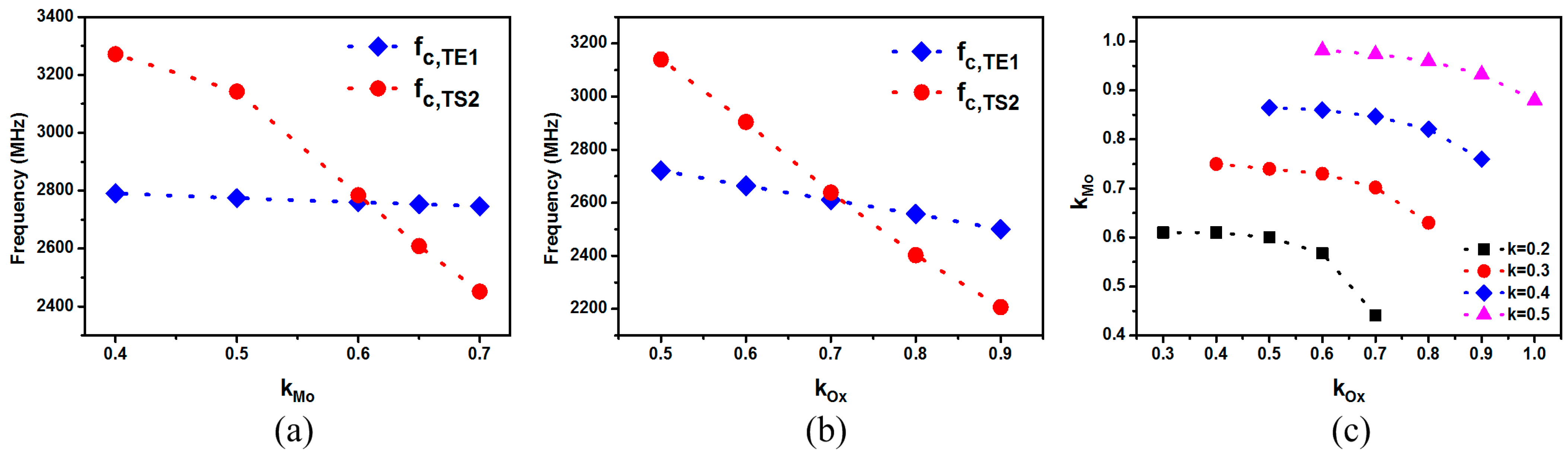
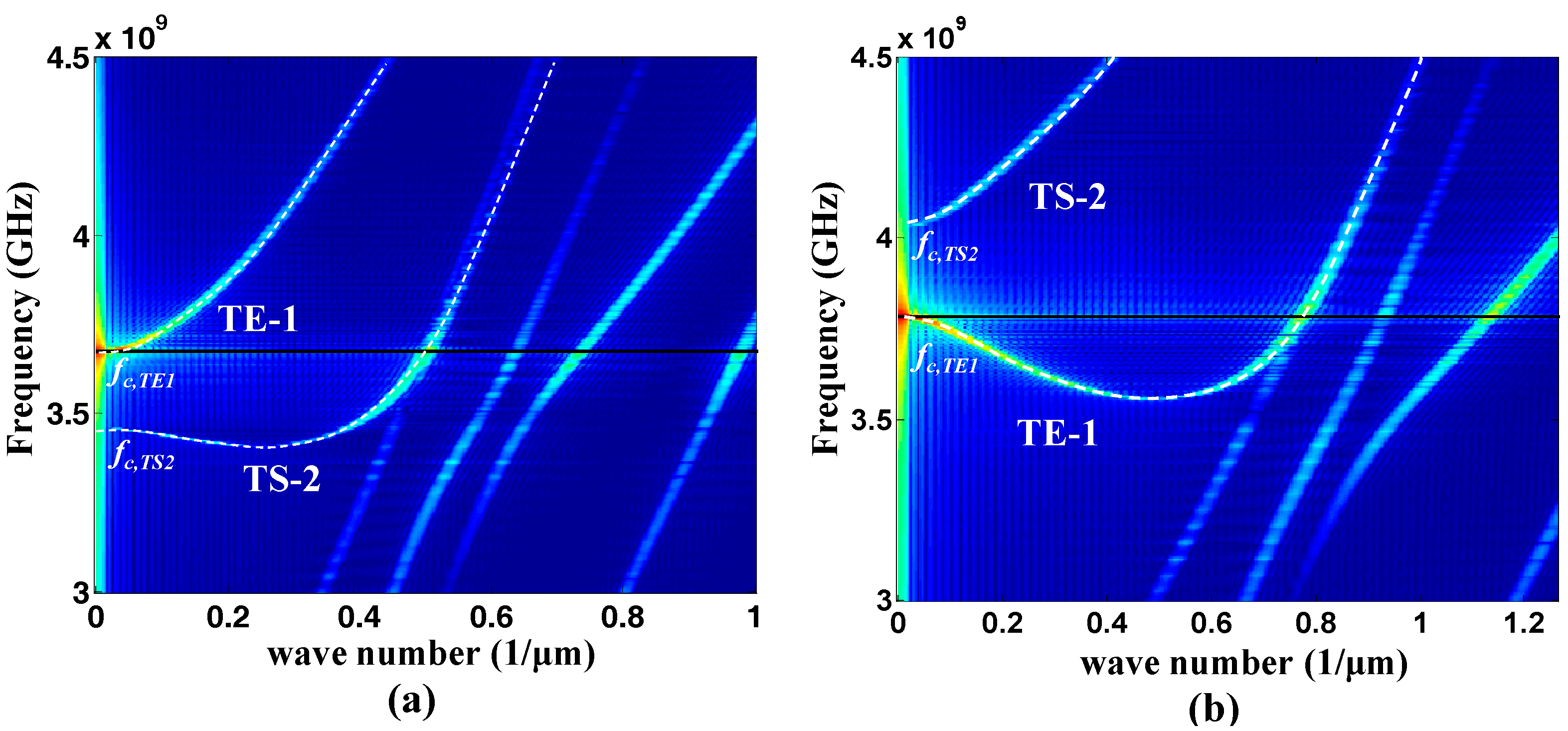
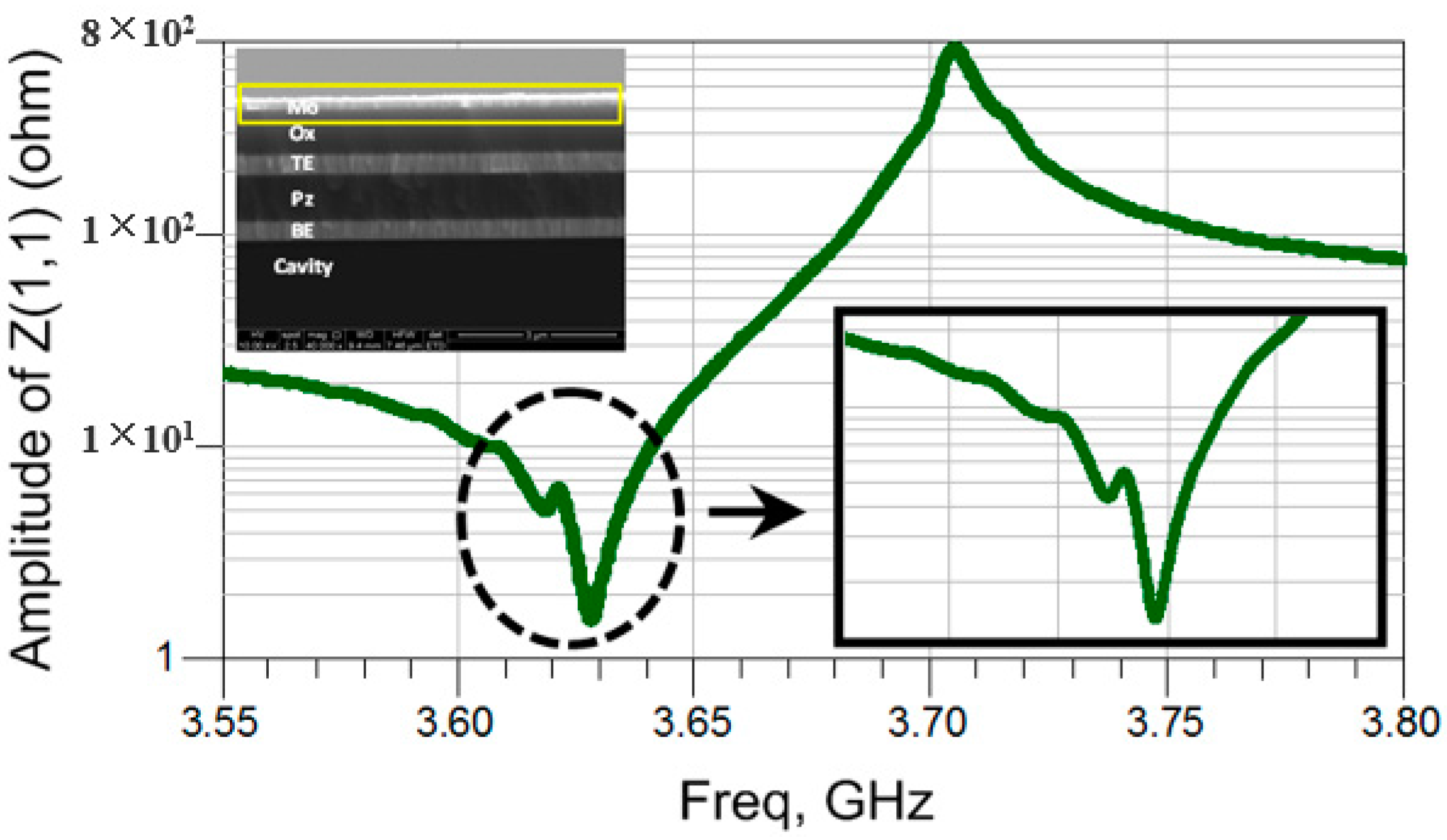
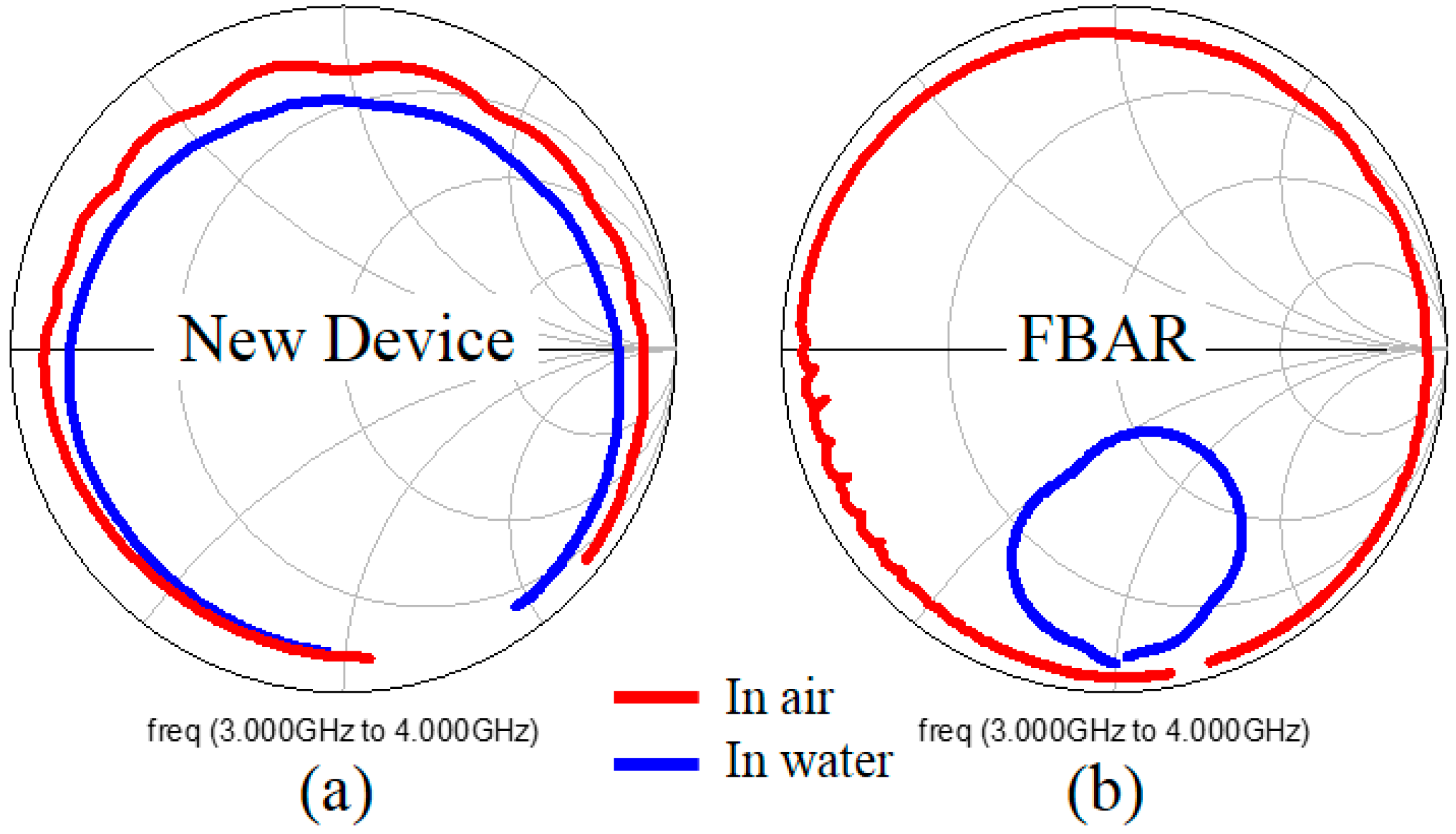
3. Results and Discussion
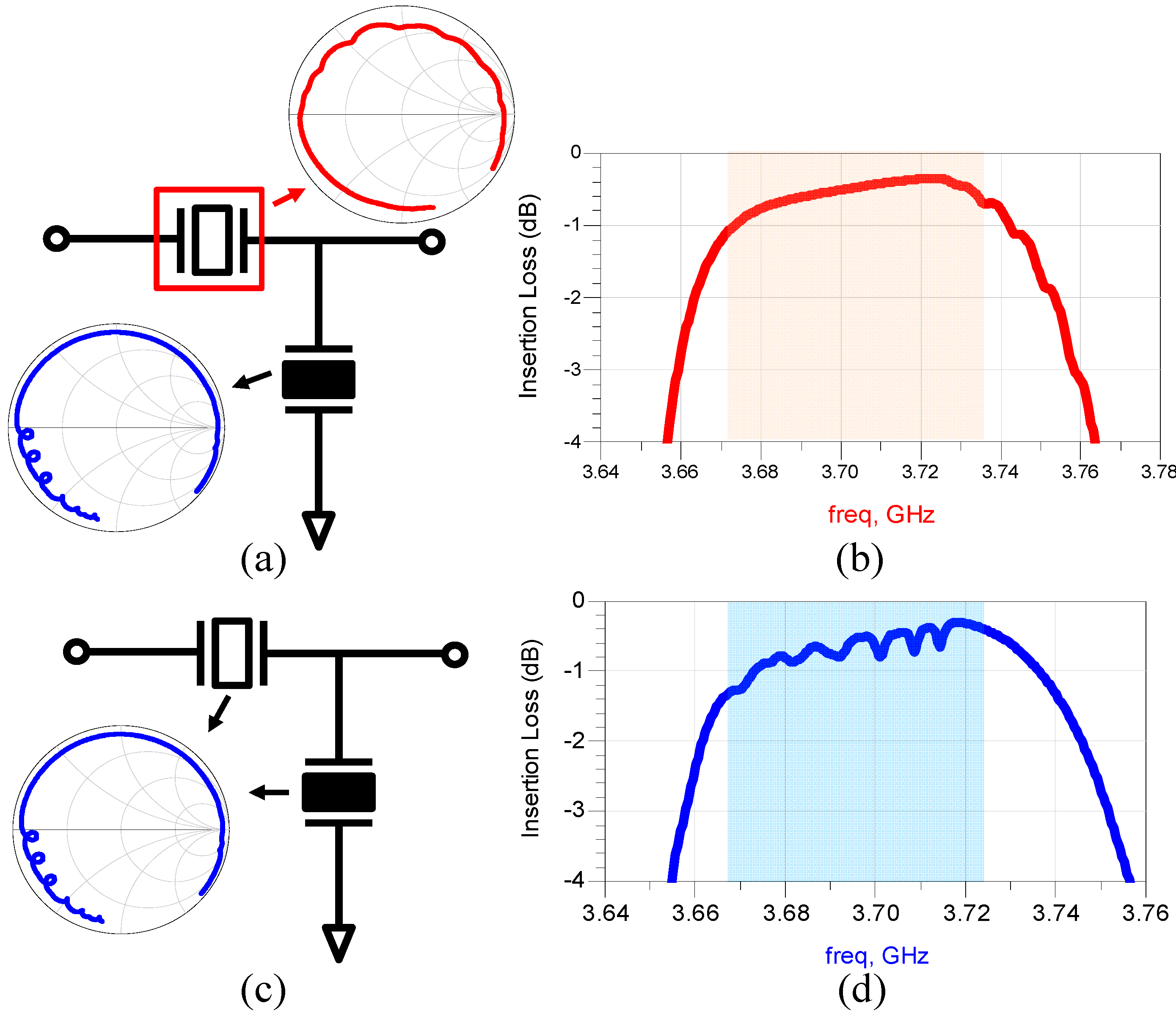
The scanning electron microscope (SEM) images of the top and the cross-sectional view of a fabricated resonator device are shown in Figure 5a,b. The scattering parameters of the resonator are measured with a ground-signal-ground (GSG) probe and a vector network analyzer on wafer level. One-port calibration with short, open, and load standards is applied with the reference plane at the probe tips. The electrical responses of the device are depicted in Figure 5c,d. From the figures, it is known that the spurious modes only appear in frequency range higher than fs, presenting a typical characteristic of the type I dispersion, which coincides with the theoretical predictions and the FEM simulations. The measured k2t,eff of the device is 4.7%, and the Q factor at fs is 1500. Since the energy in reflection layers can not be converted into the electrical energy, which decreases the electromechanical conversion efficiencies, the k2t,eff of the device is smaller than that of the FBAR. The Qs is slightly lower than that of the conventional FBAR [16], which is mainly due to the the energy leakages and the damping losses of the additional reflection layers.
Since reflection layers are on the top of the device, it is feasible to post tune the dispersion relations though the fabrication is accomplished. The thickness of the top reflection layer is thinned from 5000 Å to 1000 Å, and the measured input impedance is plotted in Figure 6. The spurious modes are in frequencies less than fs, indicating that the dispersion relations are changed, and it has been transferred to a type II dispersion from a type I property. When the thicknesses of both reflection layers are decreased to zero, the device becomes a traditional FBAR. From this point, an FBAR can be recognized as one of the devices among them.
Figure 5. Scanning electron microscope (SEM) images of (a) the top and (b) cross-sectional view of the fabricated device; (c) The input impedance curve and (d) the Smith circle of the resonator device.
Micromachines 06 01306 g005
Figure 6. The measured impedance data of the device with a thinner top reflection layer. The inset is the SEM image of the stack.
Micromachines 06 01306 g006
In filter applications, Resonators are electrically connected in a ladder or a lattice topology. They are marked as series resonators or shunt resonators according to their positions in the topology. In conventional FBAR filters, spurious modes below fs in series resonators give rise to ripples in the pass band (Figure 7c,d). If type II resonators with the same area are replaced by type I resonators in the series branch, the ripples can be moved to the margin of the pass band, recovering the flatness in most of the pass band (Figure 7a,b). The out-of-band rejection level is influenced by the area ratio of the shunt resonators to the series ones. Since the resonator areas are not changed, the substitution between types can maintain the rejection level in the out-of-band, and meanwhile suppress ripples in the pass band effectively. In the realization of the filter building, as the thicknesses of the reflection layers dominate the dispersion types, both type resonators can be realized in one filter by introducing different thicknesses of reflectors. As the reflectors are on the top of the device, it is convenient to fabricate two different thicknesses of them in different resonators by typical MEMS processes, coming to the implementation of a filter with both dispersion type resonators in it. Since the k2t,eff of the device is slightly lower, it is preferable to employ the device in filters with a narrow bandwidth.
Figure 7. (a) The schematic structure and (b) the simulated pass band performance of a primary ladder filter composed by a type I series resonator and a type II shunt resonator; (c) The schematic structure and (d) the simulated pass band performance of a primary ladder filter composed by a type II series resonator and a type II shunt resonator.
Micromachines 06 01306 g007
In addition, the new device is also tested for sensing applications. It was reported that the minimum detectable mass (or LOD) is inversely proportional to the Q value of the device [4], thus the high Q of the device further contributes to minor LOD of the sensor in biochemical sensing applications. The novel device is measured in both air and water conditions, and Figure 8a shows the performances in a Smith chart. The Q circle in water shrinks by a little scale compared to that in air. The Qs is 1500 in air, and 700 in water. The Q value in water is almost half of that in air. For comparison, an FBAR device is also tested in both environments, and the electrical performances are compared in Figure 8b. The Qs in air is over 1000, whereas it declines to less than 10 in water. The new device can keep a high Q in water, due to the two reflection layers on the top, which act as an isolator to prevent energy leakage into the water. Therefore, the novel device tends to have a better LOD.
Since the reflection layers act as a Bragg reflector, the top surface of the Mo reflection layer is insensitive to mass variations, leading to a mediocre LOD value. To solve this issue, we can adopt a localized sensing method [17]. If we punch a hole at the center of the device in the two reflection layers, the little center area of the top electrode (TE) can be accessed, which is highly sensitive to mass variations. The exposed TE area is used for mass detection, and the reflection layers around act as the energy protector to guarantee the high Q of the device in the liquid environment.
Figure 8. Electrical performances of (a) the new device and (b) the FBAR device measured in air and in water.
Micromachines 06 01306 g008

4. Conclusions

A new structure of BAW resonator is presented in this paper. A Transfer Matrix method is applied to develop the computational modeling of the acoustic waves in the device. The dispersion types are analyzed, and a set of design rules for resonators is extracted. The dispersion relations can be changed by varying the thicknesses of the reflection layers in the stack. The new structure makes it feasible to fabricate both type I and type II resonators on one chip, which provides a promising solution to improve the pass band flatness in filters. This novel device also presents a high Q value in a liquid environment, which has great potential for real time measurements in liquids in biochemical sensing applications.

Supplementary Materials

Supplementary materials can be accessed at: https://www.mdpi.com/2072-666X/6/9/1306/s1.

Acknowledgments

This work was supported by Natural Science Foundation of China (NSFC No. 61176106) and the Program of Introducing Talents of Discipline to Universities (111 project No. B07014).

Author Contributions

Zhixin Zhang, Hao Zhang and Wei Pang proposed the idea; Zhixin Zhang performed the computational modeling and the theoretical analysis; Zhixin Zhang and Wei Pang performed the FEM simulations; Zhixin Zhang, Ji Liang and Hao Zhang prepared the manuscript; and Daihua Zhang and Wei Pang contributed to the discussion and gave valuable suggestions on the manuscript revision according to the referee report.

Conflicts of Interest

The authors declare no conflict of interest.

References

  1. Ruby, R.; Bradley, P.; Larson, J.; Oshmyansky, Y. PCS 1900 MHZ duplexer using thin film bulk acoustic resonators (FBARs). Electron. Lett. 1999, 35, 794–795. [Google Scholar] [CrossRef]
  2. Ylilammi, M.; Ella, J.; Partanen, M.; Kaitila, J. Thin film bulk acoustic wave filter. IEEE Trans. Ultrason. Ferroelectr. Freq. Control 2002, 49, 535–539. [Google Scholar] [CrossRef] [PubMed]
  3. Qiu, X.; Tang, R.; Zhu, J.; Oiler, J.; Yu, C.; Wang, Z.; Yu, H. The effects of temperature, relative humidity and reducing gases on the ultraviolet response of ZnO based film bulk acoustic-wave resonator. Sens. Actuators B Chem. 2011, 151, 360–364. [Google Scholar] [CrossRef]
  4. Pang, W.; Zhao, H.; Kim, E.S.; Zhang, H.; Yu, H.; Hu, X. Piezoelectric microelectromechanical resonant sensors for chemical and biological detection. Lab Chip 2012, 12, 29–44. [Google Scholar] [CrossRef] [PubMed]
  5. García-Gancedo, L.; Zhu, Z.; Iborra, E.; Clement, M.; Olivares, J.; Flewitt, A.; Milne, W.; Ashley, G.; Luo, J.; Zhao, X. Aln-based baw resonators with CNT electrodes for gravimetric biosensing. Sens. Actuators B Chem. 2011, 160, 1386–1393. [Google Scholar] [CrossRef] [Green Version]
  6. Zhao, X.; Pan, F.; Ashley, G.M.; Garcia-Gancedo, L.; Luo, J.; Flewitt, A.J.; Milne, W.I.; Lu, J.R. Label-free detection of human prostate-specific antigen (HPSA) using film bulk acoustic resonators (FBARs). Sens. Actuators B Chem. 2014, 190, 946–953. [Google Scholar] [CrossRef]
  7. O’Connell, A.D.; Hofheinz, M.; Ansmann, M.; Bialczak, R.C.; Lenander, M.; Lucero, E.; Neeley, M.; Sank, D.; Wang, H.; Weides, M.; et al. Quantum ground state and single-phonon control of a mechanical resonator. Nature 2010, 464, 697–703. [Google Scholar] [CrossRef] [PubMed]
  8. Hashimoto, K.-Y. RF Bulk Acoustic Wave Filters for Communications; Artech House: Boston, MA, USA, 2009. [Google Scholar]
  9. Jose, S.; Hueting, R.; Jansman, A. On the rule of thumb for flipping the dispersion relation in baw devices. In Proceedings of the 2011 IEEE International Ultrasonics Symposium (IUS), Orlando, FL, USA, 18–21 October 2011; pp. 1712–1715.
  10. Zhou, C.; Zhang, D.; Pang, W.; Zhang, H. Spurious free and temperature stable Giga-hertz acoustic wave resonators with enhanced quality factor. In Proceedings of the Asia-Pacific Microwave Conference (APMC 2012), Kaohsiung, Taiwan, 4–7 December 2012; pp. 1286–1288.
  11. Fattinger, G.; Marksteiner, S.; Kaitila, J.; Aigner, R. Optimization of acoustic dispersion for high performance thin film baw resonators. In Proceedings of the 2005 IEEE Ultrasonics Symposium, Rotterdam, The Netherlands, 18–21 September 2005; pp. 1175–1178.
  12. Zhang, H.; Marma, M.S.; Kim, E.S.; McKenna, C.E.; Thompson, M.E. Implantable resonant mass sensor for liquid biochemical sensing. In Proceedings of the IEEE International Conference on Micro Electro Mechanical Systems, Maastricht, The Netherlands, 25–29 January 2004; pp. 347–350.
  13. Zhang, H.; Kim, E.S. Micromachined acoustic resonant mass sensor. J. Microelectromech. Syst. 2005, 14, 699–706. [Google Scholar] [CrossRef]
  14. Lowe, M.J. Matrix techniques for modeling ultrasonic waves in multilayered media. IEEE Trans. Ultrason. Ferroelectr. Freq. Control 1995, 42, 525–542. [Google Scholar] [CrossRef]
  15. Fattinger, G.G.; Tikka, P.T. Laser measurements and simulations of fbar dispersion relation. In Proceedings of the 2001 IEEE MTT-S International Microwave Symposium Digest, Phoenix, AZ, USA, 20–24 May 2001; pp. 371–374.
  16. Ruby, R. Review and comparison of bulk acoustic wave fbar, SMR technology. In Proceedings of the 2007 IEEE Ultrasonics Symposium, Vancouver, BC, Canada, 28–31 October 2007; pp. 1029–1040.
  17. Campanella, H.; Esteve, J.; Montserrat, J.; Uranga, A.; Abadal, G.; Barniol, N.; Romano-Rodriguez, A. Localized and distributed mass detectors with high sensitivity based on thin-film bulk acoustic resonators. Appl. Phys. Lett. 2006, 89, 033507. [Google Scholar] [CrossRef]

