Article

Rounding of Negative Dry Film Resist by Diffusive Backside Exposure Creating Rounded Channels for Pneumatic Membrane Valves

Polymeric Microsystems, Institute of Semiconductors and Microsystems, Technische Universität Dresden, 01062 Dresden, Germany
*
Author to whom correspondence should be addressed.
Micromachines 2015, 6(11), 1588-1596; https://doi.org/10.3390/mi6111442
Submission received: 7 September 2015 / Revised: 29 September 2015 / Accepted: 16 October 2015 / Published: 28 October 2015

Abstract

:
Processing of dry film resist is an easy, low-cost, and fast way to fabricate microfluidic structures. Currently, common processes are limited to creating solely rectangular channels. However, it has shown that rounded channels are necessary to ensure proper closing of pneumatic membrane valves for microfluidic devices. Here, we introduce a modification to the standard lithography process, in order to create rounded channels for microfluidic structures. Therefore, a diffuser element was inserted into in the optical path between the light source and glass substrate, which is then exposed through the backside, hence altering the exposure to the dry resist spatially. Characterization of the process was carried out with different exposure times, features sizes, and substrate thickness. The process modification is almost effortless and can be integrated in any lithography process.

1. Introduction

Soft lithography by Polydimethylsiloxane (PDMS) replica molding paved the way for rapid prototyping of microfluidic chips [1,2,3,4]. The fabrication of master molds varies from micro-milled [5] substrates over structured printed circuit boards (PCBs) [6,7] to photolithograpically obtained structures [8]. These methods compete in their minimal feature size and overall costs [9]. The most commonly employed method, because of its versatility in feature size range and short fabrication time, is the processing and photolithographical structuring of liquid resists, such as SU-8 [10]. SU-8 is known for a high achievable aspect ratio, chemical resistance, mechanical stability and durability [11]. However, the processing of liquid resist requires sophisticated technical equipment and a clean room environment.
Shorter production times and more cost-effective microfluidic chips can be achieved with dry film resists (DFRs), which require only minor investments in equipment and no clean room facilities. DFR technology is competitive to standard SU-8 processes in respect to feature size [12,13] and consistent height of the resist over a large substrate area [14,15]. Nevertheless, fabrication of round shaped channels in DFR technology for the realization of microfluidic membrane valves and pumps is not feasible yet, other than for SU-8 technology [16]. Gomez-Sjoberg et al. [17], who investigated the process parameters for reflowing positive resist, showed the necessity of rounded channels for proper closing of valves. However, the reflow method exclusively works for positive, liquid photoresist and relies on a tempering step after the structuring. Hereby, the resist is heated over its softening point wetting the surface. The round shape, which forms, is kept after cool-down.
Here, we present the fabrication of a diffuser element, which consecutively is employed in a photolithographical process, to produce rounded microchannels in negative DFR. Rounded channel structures were achieved by modifying the exposure of the DFR by inserting the diffuser element between the UV source and substrate, thus creating statistically distributed scattering centers for the incoming light. The altered light properties, the spatial resolution of absorption of the resist, and the exposure through the backside creates a rounded profile of the microfluidic channels. In this study we investigate the influence of a series of energy doses, different substrate thicknesses, and structural sizes. DFR Ordyl SY355 [18,19] was used throughout the entire set of experiments; however, we believe that this method can be feasible for other types of DFR as well.

2. Experimental Section

2.1. Diffuser Fabrication

First, 70 g of PDMS (RTV 615, MG Chemicals, New Mills, UK) in a ratio 10:1 was mixed with an electric stirrer for 5 min thoroughly. Subsequently, the PDMS mixture was poured into a casting mold, creating a layer thickness of 1.2 mm. The PDMS was cured without degassing in a convection oven at 60 °C for 2 h.

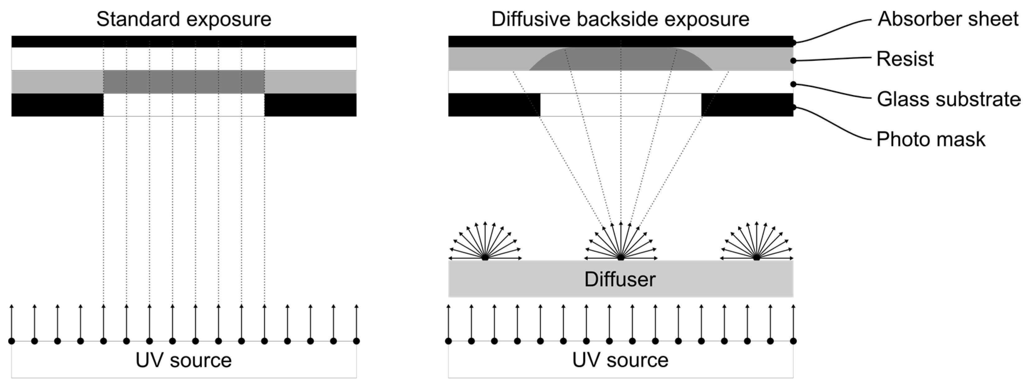
2.2. Diffusive Backside Exposure

The setup for the backside exposure can be seen in Figure 1. The diffuser element was placed on top of the UV source, covering it completely. In contrast to the standard procedure, the laminated substrate was placed, with the glass side facing toward the UV source, in the path of light. A distance between the UV source and probe of 235 mm for a homogeneous exposure was set by spacers. The substrate was then covered with an absorber sheet.
Figure 1. Exposing setup for diffusive backside exposure. The glass substrate carrying the resist was placed facing the UV source.
Micromachines 06 01442 g001
The diffuser element creates statistically distributed centers of spherical radiation, widening the radiation angle of the UV source. The spatial absorption and the radial exposure lead to a rounding of the resist structures.

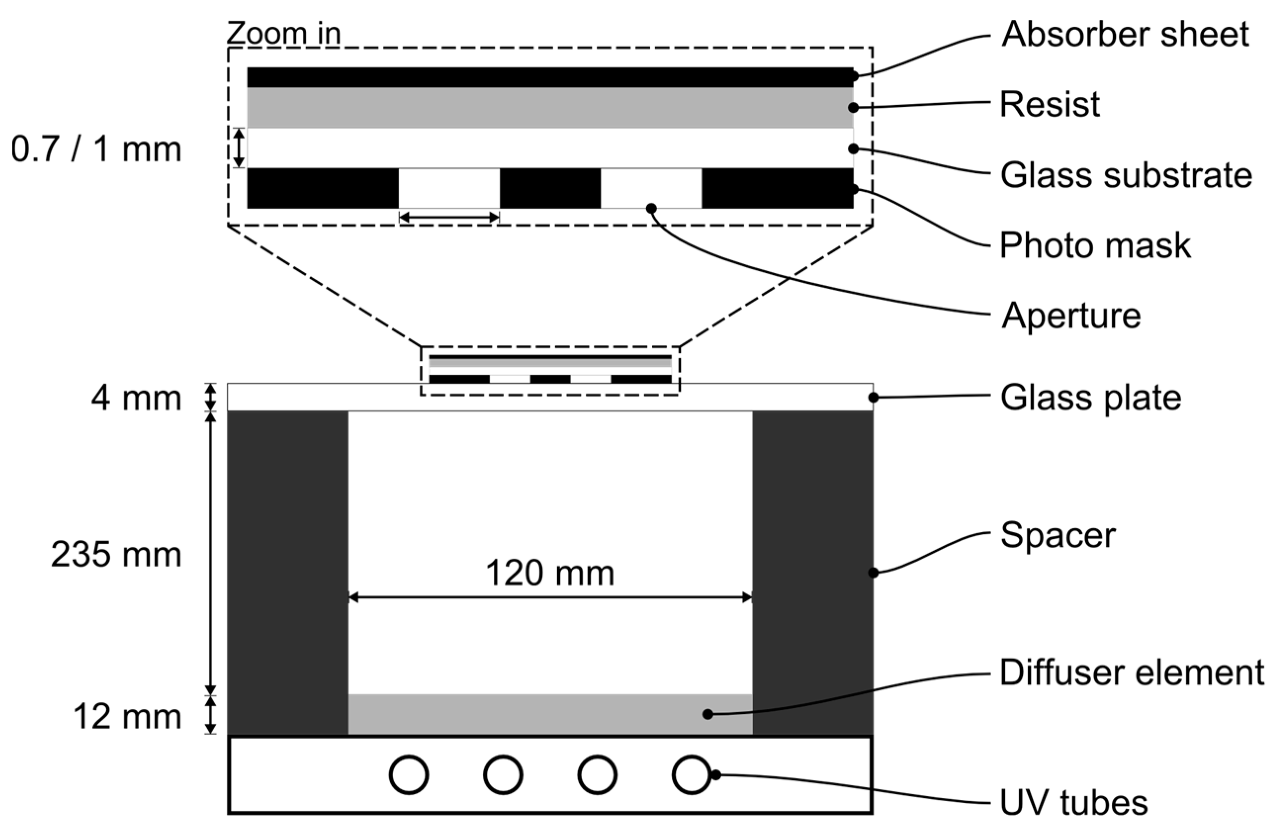
2.3. Light Energy Measurements
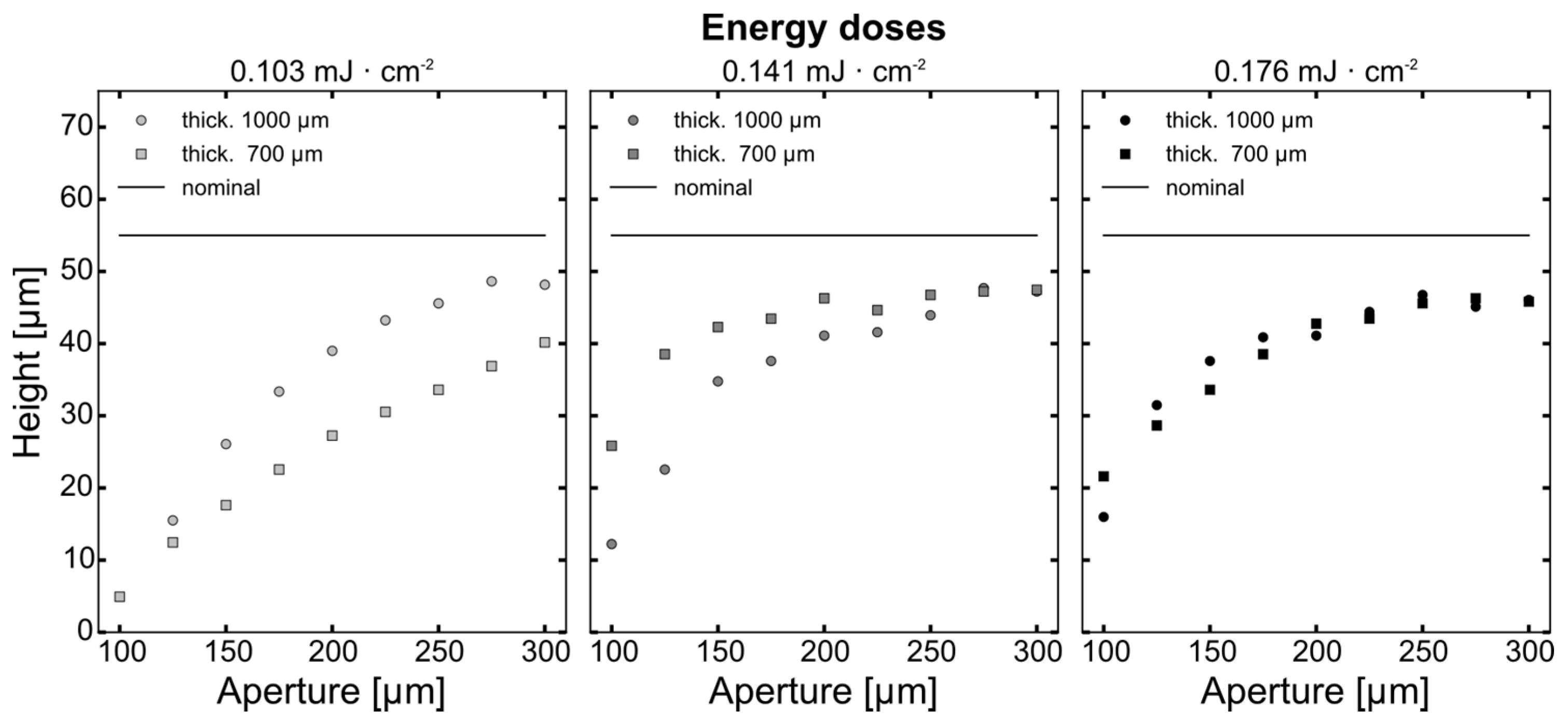
The light energy was measured behind the glass plate beneath the photo mask. The measurements were carried out with a laser power meter (FieldMax II, Coherent Inc., Santa Clara, CA, USA). The measurements in Table 1 show the effective energy dose passing through the diffuser element.
Table 1. Varied exposure times and resulting energy doses.
Exposure Time (s)240360480
Energy Dose (mJ·cm−2)0.1030.1410.176

2.4. Master Fabrication

A glass substrate (Borofloat 33, Schott AG, Mainz, Germany) with a thickness of 0.7 mm had 1.0 mm cleaned with acetone, isopropanol and distilled water and consecutively dried using nitrogen. A dehydration bake at 150 °C for 20 min was performed on a hot plate following all baking steps. A single layer of dry film resist (Ordyl SY355, Elga Europe, Nerviano, Italy) was laminated onto the substrate and soft-baked at 85 °C for 3 min. The glass substrate was backside-exposed through a polymer film mask (Electronic Packaging Laboratory, Technische Universität Dresden, Dresden, Germany) for either 240, 360, or 480 s. The according energy doses were determined as seen in Table 1. The post-exposure bake (PEB) was performed at 85 °C for 30 min. For development, the Ordyl developer and rinser (Ordyl Developer & Rinser, Elga Europe, Nerviano, Italy) was used. The substrates were developed first in used developer for 4 min and then in fresh developer for 3 min. To stop the development the substrate was put in the rinser bath for 2 min. The development was finished off with rinsing with isopropanol and distilled water. The process was completed with a hard bake at 120 °C for 1.5 h.

2.5. Profile Measurements

The resist master was molded with PDMS (RTV 615, MG Chemicals, New Mills, UK) in a ratio of 10:1 and cured at 60 °C for 3 h. PDMS shows a sufficient resolution accuracy to represent the resist structures. The cross-section was created with a sharp-edge cutting tool. A microscope (M420, Wild Heerbrugg, Heerbrugg, Switzerland) equipped with a CCD camera (DCM130E, Scopetek, Hangzhou, China) was used for documentation and data acquisition. The in-picture measurements were carried out with the open source software Fiji Is Just ImageJ [20].

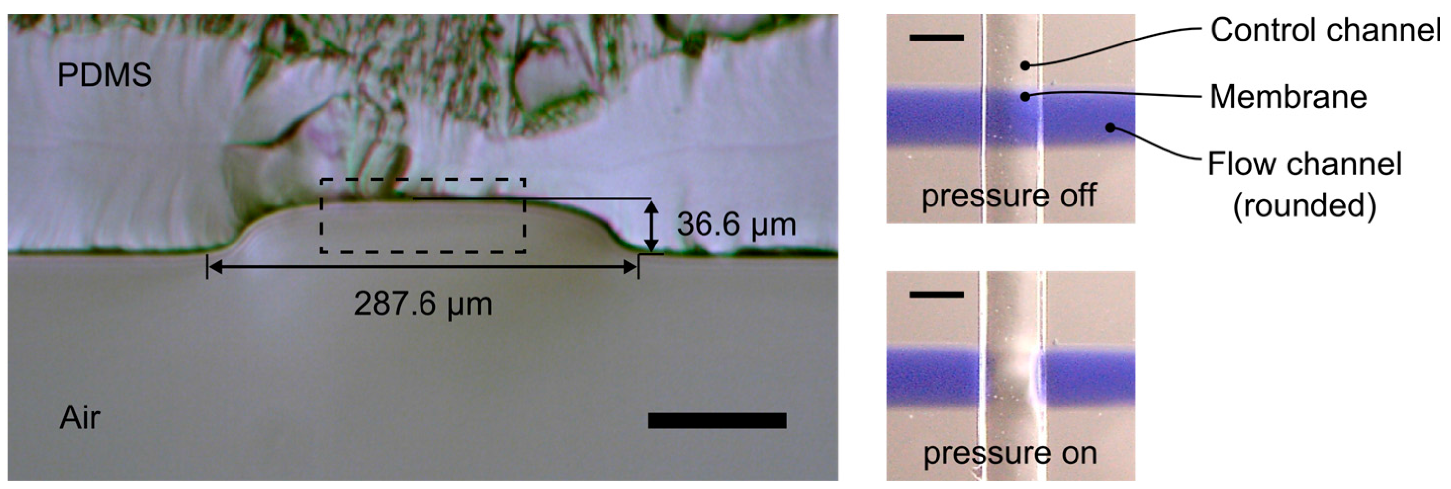
2.6. Pneumatic Valve

The pneumatic valve was fabricated by multi-layer soft lithography. The upper (control) layer was molded as explained in section 2.5, creating a 4 mm thick layer. The bottom (flow) layer was created by spin-coating PDMS (10:1) on the master. The flow layer thickness was 80 µm, creating a membrane with a thickness of 55 µm. The layers were joined via oxygen plasma bonding. The assembled chip was closed with a glass substrate also using oxygen plasma bonding. The actuation of the valve was carried out with a pressure of 1 bar.

3. Results and Discussion

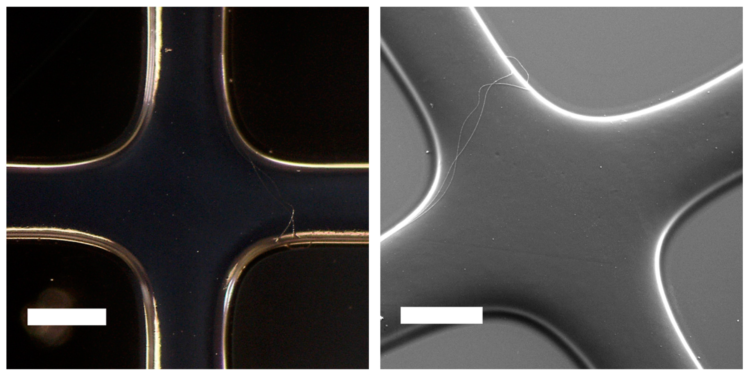
3.1. Diffuser Element and Backside Exposure

The fabrication of the diffuser element differed from the regular PDMS procedure by not de-gassing the mixture. Thoroughly stirring generated air bubbles that were encapsulated during the baking step. These air bubbles function as statistically distributed centers of scattering, propagating diffusive reflection. This effect creates light radiating evenly in every direction. It needs to be taken in account that the diffuser absorbs a fraction of the light energy, creating the need to measure the effective light energy dose still passing through, as seen in Table 1. We expect the fraction of absorbed light to increase with the thickness of the diffuser. However, the diffuser needs a minimum thickness to enable a homogeneous distribution of scattering centers.
In Figure 2, the optical path of the standard exposure with parallel light (left) versus the backside exposure with diffusive light (right) can be seen. The intensity of the diffusive light has a spatial maximum absorption in the middle of the aperture. Towards the edges, the intensity declines due to the radiation angle, reducing the absorption. This shift in intensity creates the rounding of the photoresist. The left image in Figure 2 shows the standard procedure with an exposure of the substrate from the resist side. The parallel light creates an evenly distributed intensity, which generates edges with a high steepness.
Figure 2. (Left) Optical path of the standard exposure with parallel light. (Right) Optical path of the backside exposure with diffusive light. Both with indications of intensity distribution and the spatial absorption of the resist.
Micromachines 06 01442 g002

3.2. Structure Width
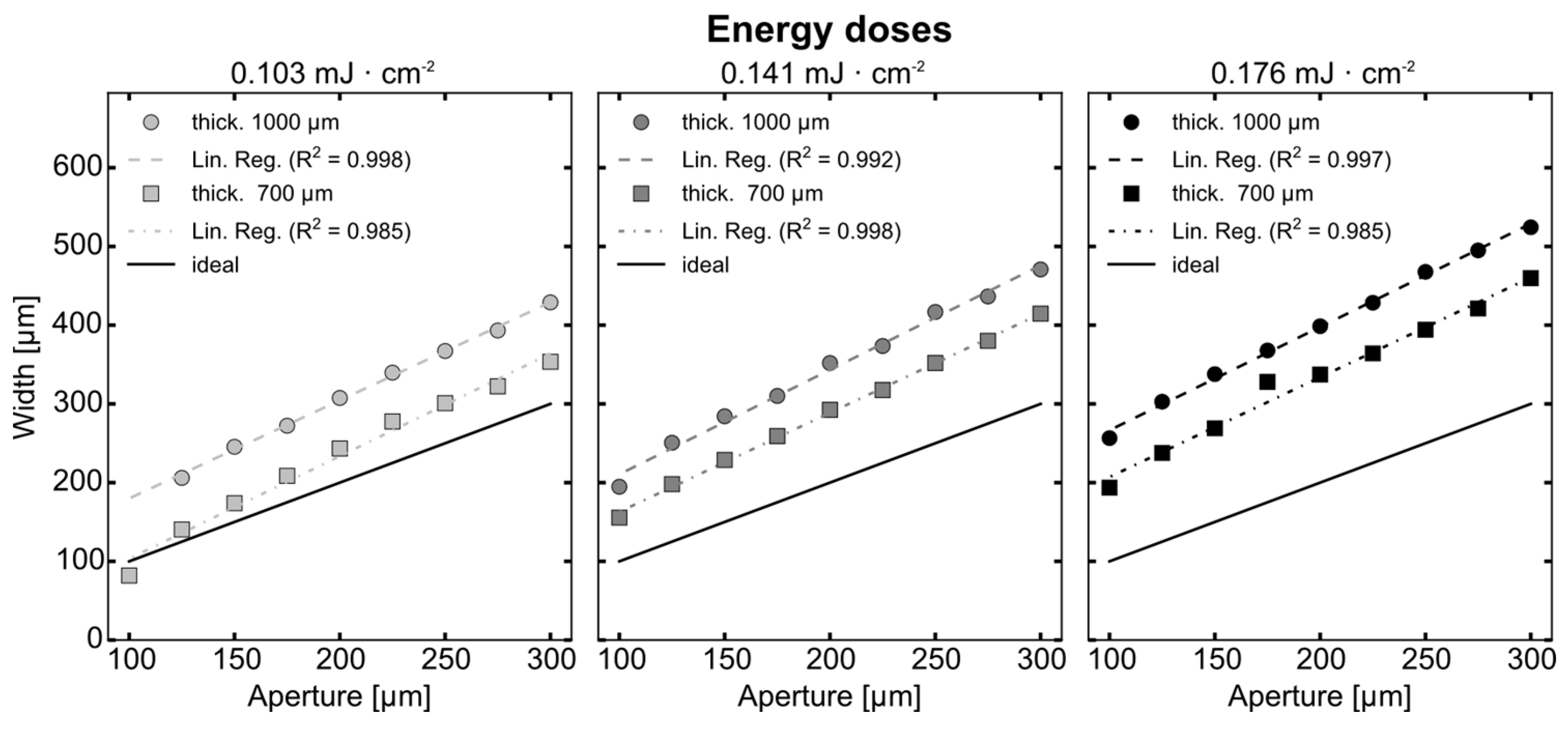
The aperture width range was set from 100 to 300 µm with a step size of 25 µm. This range seemed to be of general interest for the channel width in microfluidic application. Figure 3 shows a dark field microscope and scanning electron microscope (SEM) image of resulting DFR resist structures with rounded edges indicating the functioning of the process. Especially the image on the right (SEM image) shows the smooth rounding of the normally sharp edges.
Figure 3. Chip structure exposed at an energy dose = 0.141 mJ·cm−2 through a glass substrate thickness = 0.7 mm. (Left) Dark field microscope image of chip structure with rounded DFR (scale bar = 300 µm). (Right) Scanning electron microscope (SEM) image at 20 kV, 100-fold magnification and secondary electrons (scale bar = 200 µm).
Micromachines 06 01442 g003
In Figure 4 (left), the cross-section of a PDMS chip molded from a channel with a nominal aperture of 150 µm (dotted line) and an exposure dose of 0.141 mJ·m−2 by diffusive backlight exposure can be seen, resulting in a rounded shape of the channel. The images on the right in Figure 4 show the rounded channel (in blue) employed in a pneumatic valve. The top image is the valve in its open state. The image beneath shows the valve actuated with pressurized air. The membrane deflects down into the flow channel, displacing the blue ink and indicating the closing of the valve.
The resulting resist structures exhibit a smooth incline from the edges to the top of the channel, which is rather flat. The structure shows a change in lateral and vertical dimensions. The channel width increased by approximately 137 µm, whereas the height of the channels decreased from 55 to 36 µm. The relation between nominal aperture and measured feature width is shown in Figure 5. The measured feature width increases linearly over the aperture. Further, by fitting the measured feature width by means of linear regression shows a linear behavior of the measured feature width and mask aperture. The narrow R2-values between 0.998 and 0.985 confirm a strong linear relation.
Figure 4. (Left) Cross-section view of rounded channel molded in PDMS annotated with measured width, height and projection of the nominal channel measures. Process parameters: aperture = 150 µm, energy dose = 0.141 mJ·cm−2 and glass substrate thickness = 1.0 mm (scale bar = 100 µm). (Right) Top view of a pneumatic membrane valve utilizing a rounded flow channel (blue ink). (Right top) Valve open with no pressure applied in the control channel; (Right bottom) Valve closed with pressure applied in the control channel. Process parameters: aperture = 200 µm, energy dose = 0.103 mJ·cm−2 and glass substrate thickness = 0.7 mm (scale bar = 200 µm).
Micromachines 06 01442 g004
Figure 5. Measured structure width, linear fit, and modeled feature width over the nominal aperture width at 0.103, 0.141, and 0.176 mJ·cm−2 as well as glass substrate thicknesses of 0.7 and 1.0 mm.
Micromachines 06 01442 g005
An expected feature width was modeled as described in Equation (1):
w = m·x + n
where w is the resulting width, m corresponds to the slope, x is the mask aperture, and n is an offset.
Equation (1) evaluates the relation between mask aperture and feature width. The expected feature width (ideal) as seen in Figure 5 clearly lies under the achieved values in all cases. The slope of the linear fit is in the range of 1.25 and 1.33 with a mean of 1.29 with a standard deviation of 0.09 (Table 2). The average slope is steeper by the factor of 1.29 compared to the ideal slope, which has a slope of 1.0. The ideal curve shows perfect conformity of designed aperture width and resulting width. Further, an offset of the linear fit can be observed, depending on the thickness of the substrate and the energy dose. The offset is higher for a substrate thickness of 1.0 mm and increases with the energy dose. The difference between the expected feature width and the measured one is minimal for a substrate thickness of 0.7 mm and an energy dose of 0.103 mJ·cm−2. Overall, an increase in width for each aperture can be observed. Even though a difference between the expected feature and resulting feature width was found, due to the linear behavior and a simple model, the difference can be calculated respectively.
Table 2. Values of the linear regression for a variation of fabrication parameter: m—slope; n—offset of the linear function; R2—coefficient of determination.
Thickness (mm)Energy Dose (mJ·cm−2)m (-)n (µm)R2 (-)
1.00.1031.2555.300.998
0.70.1031.30−27.030.985
1.00.1411.3377.920.992
0.70.1411.2637.040.998
1.00.1761.31135.280.997
0.70.1761.2780.320.985
-Average1.29--
-Deviation0.09--

3.3. Structure Height

The cross-section in Figure 4 shows the characteristic shape of a rounded channel. It becomes apparent that the attained height exhibits a difference in comparison to the nominal height of the DFR Ordyl SY355, which is nominally 55 µm. The graph in Figure 6 shows the resulting heights over the nominal aperture width according to the energy doses. Over the increasing aperture, the height also increases, but, in contrast to the width, in a non-linear manner. The height converges to a saturation of about 48 to 50 µm, which indicates the spatial limit of the resist’s height. Comparing the nominal height of 55 µm to the saturation height, a difference of about 5 to 7 µm can be noted. This difference can be explained by a shrinkage of the resist after the hard bake. The saturation in the graph indicates that the maximal attainable height was achieved. Small structures show a significantly lower height down to 10 µm and below compared to structures with a wider aperture. Though with an increase in energy dose the height of the structures also increase, shifting the point of saturation to the left, towards small apertures. This means that an increase in energy dose will produce a better resolution of the features size and an increase the height. While an energy dose of 0.103 mJ·cm−2 shows no structures below 125 µm, an increase in energy dose to 0.176 mJ·cm−2 shows structures with a height of 17 µm.
The substrate thickness shows no influence at the highest energy dose of 0.176 mJ·cm−2, while at lesser exposing energy, a difference of the attained heights was of higher significance. Especially at the lowest energy dose, a clear difference between the two glass substrates can be made out.
Figure 6. Measured structure height over the nominal aperture width at 0.103, 0.141, and 0.176 mJ·cm−2 as well as glass substrate thicknesses of 0.7 and 1 mm. The nominal height of the resist is 55 µm.
Micromachines 06 01442 g006

4. Conclusions

The fabrication of the diffuser is a straightforward procedure, which only requires basic PDMS technology. The process modifications of inserting the diffuser element and exposing through the backside can be realized with minor expense. The method was able to produce a rounded structure, which can be employed in pneumatic, microfluidic channels, enabling a valve to close in a reasonable pressure range.
The structures also exhibited, besides the change in shape, a change in dimensions. To evaluate the structural alterations, the parameters of resulting width and resulting height were measured. Width and height are most suitable because of their central importance in the design of microfluidic devices.
The data stated a certain divergence between nominal values and resulting values regarding the width and the height. This variation of nominal values and resulting values is already known from the reflowing of positive photo resist [17,21], although the causing effects differ. Even though these divergences exist, our results suggest a good pre-determination of the process outcome. With a simple linear model, the resulting structure width can be calculated and respectively interpolated. An additional analysis displaying the resulting width and an according fit over the energy dose is provided as supplementary material.
The relation between aperture width and height does not seem as trivial, but our data allows an estimate of the resulting height as well. The data allows the fabrication of multi-level height structures on one substrate without the need for a multi-level resist process, which eventually requires sophisticated aligning equipment.
The experiments suggest that the substrate thickness has a major influence in the conformity regarding the width of the structures. The thinner the substrate, the better the conformity of the resulting width respective to the designated width. Combining this with a smaller aperture and an increase in energy dose, more spherical cross-sections can be achieved.
Our findings between the relation of how substrate thickness, energy dose and nominal height influence the out-coming structure regarding its width and height are meant as guidelines for designers of microfluidic systems. Considering the effects of the process parameters, the out-coming structures can already be estimated during the design process. The manifestation of differing heights for varying channel widths has already found functional usage in the generation of droplets [22].
The process modification comes along effortlessly and constitutes a handy advance for DFR technology in general, enabling the fabrication of rounded features.

Supplementary Materials

The following are available online at https://www.mdpi.com/2072-666X/6/11/1442/s1. Figure S1: Measured structure width and modeled feature width over the energy dose for the aperture range 100 µm to 300 µm in 25 µm steps, and with respect to the substrate thickness of 0.7 mm and 1.0 mm. Table S1: Values of the linear regression of the resulting width over the exposed energy dose: m—slope; n—offset of the linear function; R2—coefficient of determination.

Acknowledgments

Thanks goes to Gerald Hielscher from the Electronic Packaging Laboratory, Technische Universität Dresden for the straightforward supply of photo masks. We also acknowledge the support of Enrico Langer from the Institute of Semiconductors and Microsystems, Technische Universität Dresden for his support at the scanning electron microscope. Further we thank the DFG Research Training Group “Hydrogel-Based Microsystems” for financial support.

Author Contributions

Philipp Frank fabricated the diffuser element, conducted the experiments and the data analysis. Sebastian Haefner supported the design and the conduction of the experiments. Georgi Paschew set up the optical model. Andreas Richter supervised and supported the project. All authors reviewed the manuscript.

Conflicts of Interest

The authors declare no conflict of interest.

References

  1. Xia, Y.N.; Whitesides, G.M. Soft lithography. Annu. Rev. Mater. Sci. 1998, 37, 551–575. [Google Scholar]
  2. Duffy, D.C.; McDonald, J.C.; Schueller, O.J.A.; Whitesides, G.M. Rapid Prototyping of Microfluidic Systems in Poly(dimethylsiloxane). Anal. Chem. 1998, 70, 4974–4984. [Google Scholar] [CrossRef] [PubMed]
  3. Fan, H.; Lu, Y.; Stump, A.; Reed, S.; Baer, T.; Schunk, R.; Perez-Luna, V.; Lopez, G.; Brinker, C. Rapid prototyping of patterned functional nanostructures. Nature 2000, 405, 56–60. [Google Scholar] [CrossRef] [PubMed]
  4. Qin, D.; Xia, Y.; Whitesides, G.M. Soft lithography for micro- and nanoscale patterning. Nat. Protoc. 2010, 5, 491–502. [Google Scholar] [PubMed]
  5. Forfang, W.B.D.; Conner, T.G.; You, B.H.; Park, T.; Song, I.H. Fabrication and characterization of polymer microprisms. Microsyst. Technol. 2014, 20, 2071–2077. [Google Scholar] [CrossRef]
  6. Abdelgawad, M.; Watson, M.W.L.; Young, E.W.K.; Mudrik, J.M.; Ungrin, M.D.; Wheeler, A.R. Soft lithography: Masters on demand. Lab Chip 2008, 8, 1379–1385. [Google Scholar] [PubMed]
  7. Li, C.W.; Cheung, C.N.; Yang, J.; Tzang, C.H.; Yang, M. PDMS-based microfluidic device with multi-height structures fabricated by single-step photolithography using printed circuit board as masters. Analyst 2003, 128, 1137–1142. [Google Scholar] [CrossRef] [PubMed]
  8. Stroock, A.D.; Whitesides, G.M. Components for integrated poly (dimethylsiloxane) microfluidic systems. Electrophoresis 2002, 23, 3461–3473. [Google Scholar] [CrossRef] [PubMed]
  9. Vulto, P.; Glade, N.; Altomare, L.; Bablet, J.; Tin, L.D.; Medoro, G.; Chartier, I.; Manaresi, N.; Tartagni, M.; Guerrieri, R. Microfluidic channel fabrication in dry film resist for production and prototyping of hybrid chips. Lab Chip 2005, 5, 158–162. [Google Scholar] [CrossRef] [PubMed]
  10. Xu, B.; Arias, F.; Brittain, S.; Zhao, X.; Grzybowski, B.; Torquato, S.; Whitesides, G.M. Making negative Poisson’s ratio microstructures by soft lithography. Adv. Mater. 1999, 11, 1186–1189. [Google Scholar] [CrossRef]
  11. Campo, A.D.; Greiner, C. SU-8: A photoresist for high-aspect-ratio and 3D submicron lithography. J. Micromech. Microeng. 2007, 17, R81. [Google Scholar] [CrossRef]
  12. Stephan, K.; Pittet, P.; Renaud, L.; Kleimann, P.; Morin, P.; Ouaini, N.; Ferrigno, R. Fast prototyping using a dry film photoresist: Microfabrication of soft-lithography masters for microfluidic structures. J. Micromech. Microeng. 2007, 17, N69. [Google Scholar] [CrossRef]
  13. Wangler, N.; Gutzweiler, L.; Kalkandjiev, K.; Müller, C.; Mayenfels, F.; Reinecke, H.; Zengerle, R.; Paust, N. High-resolution permanent photoresist laminate TMMF for sealed microfluidic structures in biological applications. J. Micromech. Microeng. 2011, 21, 095009. [Google Scholar] [CrossRef]
  14. Vulto, P.; Huesgen, T.; Albrecht, B.; Urban, G.A. A full-wafer fabrication process for glass microfluidic chips with integrated electroplated electrodes by direct bonding of dry film resist. J. Micromech. Microeng. 2009, 19, 077001. [Google Scholar] [CrossRef]
  15. Jiang, L.T.; Huang, T.C.; Chang, C.Y.; Ciou, J.R.; Yang, S.Y.; Huang, P.H. Direct fabrication of rigid microstructures on a metallic roller using a dry film resist. J. Micromech. Microeng. 2008, 18, 015004. [Google Scholar] [CrossRef]
  16. Futai, N.; Gu, W.; Takayama, S. Rapid prototyping of microstructures with bell-shaped cross-sections and its application to deformation-based microfluidic valves. Adv. Mater. 2004, 16, 1320–1323. [Google Scholar] [CrossRef]
  17. Fordyce, P.M.; Diaz-Botia, C.A.; DeRisi, J.L.; Gomez-Sjoberg, R. Systematic characterization of feature dimensions and closing pressures for microfluidic valves produced via photoresist reflow. Lab Chip 2012, 12, 4287–4295. [Google Scholar] [CrossRef] [PubMed]
  18. Elga Europe. Ordyl SY300: Product Data Sheet. Available online: http://www.elgaeurope.it/user/download_ctg.aspx?TIPO=F&FILE=OBJ00078.PDF&NOME=Product+Data+Sheet_SY300.pdf (accessed on 1 September 2014).
  19. Vulto, P.; Glade, N.; Altomare, L.; Bablet, J.; Medoro, G.; Leonardi, A.; Romani, A.; Chartier, I.; Manaresi, N.; Tartagni, M.; et al. Dry film resist for fast fluidic prototyping. In Proceedings of the 8th International Conference on Miniaturized Systems for Chemistry and Life Sciences, Malmö, Sweden, 26–30 September 2004; Royal Society of Chemistry: London, UK; Volume 2, pp. 43–45.
  20. Schindelin, J.; Arganda-Carreras, I.; Frise, E.; Kaynig, V.; Longair, M.; Pietzsch, T.; Preibisch, S.; Rueden, C.; Saalfeld, S.; Schmid, B.; et al. Fiji: An open-source platform for biological-image analysis. Nat. Meth. 2012, 9, 676–682. [Google Scholar] [CrossRef] [PubMed]
  21. O’Neill, F.T.; Sheridan, J.T. Photoresist reflow method of microlens production Part I: Background and experiments. Opt. Int. J. Light Electron. Opt. 2002, 113, 391–404. [Google Scholar] [CrossRef]
  22. Lai, D.; Frampton, J.P.; Sriram, H.; Takayama, S. Rounded multi-level microchannels with orifices made in one exposure enable aqueous two-phase system droplet microfluidics. Lab Chip 2011, 11, 3551–3354. [Google Scholar] [CrossRef] [PubMed]

