1. Introduction
Graded Reflectivity Mirrors (GRM) have been used in laser systems as beam quality and mode controllers, as well as output beam shapers [
1,
2]. The typical method of creating a spatially varying reflectance or transmittance profile is achieved by spatially varying thin dielectric film non-absorbers [
3,
4]. The fabrication method for such spatially varying dielectric film layers employs a rotating mask in the thin film deposition process. This has the effect of varying the thickness of the deposition as well as, creating axial symmetric devices, over the coated device areas.
Space-variant guided-mode resonant filters (GMRF) have been previously presented as an alternative to conventional GRM [
5,
6]. Standard and novel micro-fabrication techniques are used to fabricate these optical devices. The structural parameters of a standard GMRF are varied in three dimensions across the device volume to create a Graded Reflectivity Mirror. Previous work has demonstrated GMRF based GRM with axially symmetric reflectivity. In addition, space variant GMRFs have been created using similar techniques used to create GRMs, and thus suffer from the same limitations in the type of reflectance or transmittance profiles that can be achieved [
7]. In this paper, we will demonstrate that our optical devices are also capable of non-axially symmetric structural profiles, which lead to mirror-type symmetries in optical performance.
GMRF’s combine planar slab waveguides and sub-wavelength (or near sub-wavelength) gratings (SWG) to create spectral reflection filters [
8]. An optical resonance occurs if the transverse propagation constant of a diffracted order via the grating layer, matches the propagation constant of a guided mode in the planar waveguide. When incident light meets this resonance condition, evanescent diffraction orders from the sub-wavelength resonance grating will couple energy into the guided mode(s) of the waveguide. The planar waveguide is designed to be of the “leaky” type, from the side of the superstrate, where the SWG is located. The guided modes then re-couple (leak) towards the initial light source direction. When light does not meet these resonance conditions, the evanescent diffracted orders interfere destructively, allowing only the 0
th diffracted order to propagate in the original direction. The period of the SWG is chosen such that all of the diffracted orders, except the 0
th, are evanescent, meaning that the scale of the grating period is smaller than the incident light wavelength. The resonance of the GMRF is a function of the optical properties of the dielectric materials used: the thickness of the dielectric layers, the period of the SWG, and the fill-fraction (duty-cycle) of the SWG. The sensitivity of GMRFs to the various structural and optical parameters has been exploited to create various types of GMRFs where the resonance condition can be tuned by modifying one or more of these parameters [
9,
10,
11,
12]. The resonance of a GMRF can also be tuned by adjusting the angle of incidence of the light source [
13]. In addition, the sensitivity of the resonance condition of GMRFs to the structural and optical parameters can be applied to sensors [
14].
Figure 1.
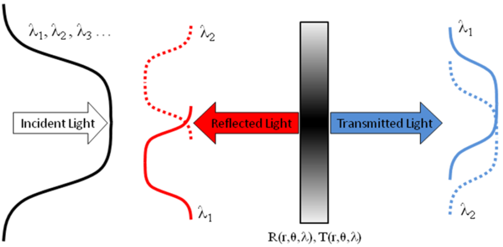
Conceptual performance of a space variant GMRF.
Figure 1.
Conceptual performance of a space variant GMRF.
A space variant GMRF can be realized by slowly varying the lattice properties, modifying the resonant response as a function of spatially localized parameters. The conceptual performance of such a device is shown in
Figure 1. The device proposed in this paper will vary the fill fraction of the SWG as a function of angle about the axial center of the device. The transmission and reflection of this device will then be a function of local position within the SWG and the incident wavelength.
2. Simulation Results
The grating structure used for this device is a hexagonal lattice, so that the resonance conditions of the GMRF are polarization independent, for normal incidence of the light wave. The waveguide and SWG layers are composed of Silicon Nitride (Si
xN
y) and Silicon Oxide (SiO
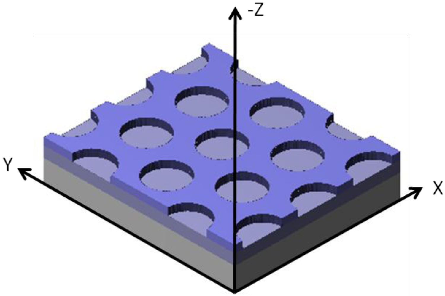
x), respectively. A three-dimensional representation of a conventional GMRF, with a fixed spatial period and grating duty cycle, is shown in
Figure 2. The period of the grating is 1.15 µm; the thickness of the silicon oxide is 240 nm; and the thickness of the wave-guiding layer is 375 nm. The SWG is etched 170 nm into the silicon oxide layer. The substrate is a 1 mm thick fused silica wafer.
Figure 2.
3D representation of a GMRF with a hexagonal lattice.
Figure 2.
3D representation of a GMRF with a hexagonal lattice.
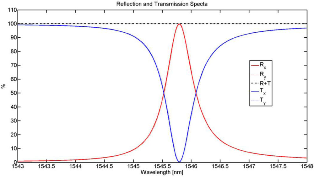
Figure 3.
RCWA results of a fixed period and duty-cycle GMRF. The Rx and Ry (and Tx and Ty) represent the reflection (and transmission) spectra from the polarizations in the x and y directions.
Figure 3.
RCWA results of a fixed period and duty-cycle GMRF. The Rx and Ry (and Tx and Ty) represent the reflection (and transmission) spectra from the polarizations in the x and y directions.
Rigorous Coupled Wave Analysis (RCWA) was used to optimize and simulate the spectral performance of the device [
15]. RCWA is a semi-analytical model used to analyze infinitely periodic, dielectric index structures.
Figure 3 shows the RCWA results for a GMRF described above with a 400 nm hole radius. The resonance is located at 1,545.8 nm with a full-width at half-maximum (FWHM) linewidth of 0.57 nm. The
Rx and
Ry (and
Tx and
Ty) represent the reflection (and transmission) spectra from the polarizations in the
x and
y directions, as shown in
Figure 2, respectively. The slight difference in the spectra between the two polarization states is a result of numerical errors in simulating the unit cell geometry.
The resonance condition in a GMRF is produced by a phase matching condition between the SWG and the leaky modes in the waveguide. In a spatially varying GMRF, the rate at which the leaky-modes re-couple energy to the 0
th diffracted order can affect the properties of the reflected beam. Therefore, the decay length of the leaky modes was studied by approximating the hexagonal GMRF as a 1D ruled grating GMRF using effective medium theory. A one-dimensional structure was constructed with the same period and layer thicknesses as the original GMRF, but the fill-fraction and depth of the SWG was modified to match the behavior of the 2D GMRF. The method of lines was used to calculate the decay rate of the fundamental mode from the
S21 scattering coefficient [
16]. Based on this analysis, the decay length was found to be 30 µm.
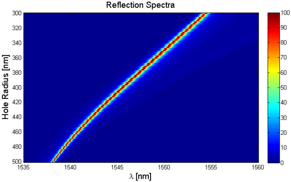
Figure 4.
Spectral response of the GMRF as a function of holes radii.
Figure 4.
Spectral response of the GMRF as a function of holes radii.
As stated previously, the resonance condition for a GMRF is a function of the many structural and optical parameters of the device. In order to achieve a spatial variation of the resonance condition, one or more of these parameters needs to be spatially modulated. For this paper, the fill fraction or the diameter of the holes in the GMRF lattice was chosen as the parameter variable. It is assumed and is shown, that the resonance condition is a function of the local structural properties across the entire surface of the device. Under this assumption, the impact of the spatial modulation can be investigated. Modulation of the fill-fraction of the SWG changes the effective optical refractive index of the SWG. The SWG serves as a portion of the cladding of the waveguide, and changes to the effective index also change the guided modes conditions. Thus, a change in the fill fraction of the SWG will perturb the resonance conditions of the GMRF and modify the spectral response of the micro-optical device.
Figure 4 shows that a variation of 300 nm to 500 nm in the hole radius, results in a continuous spectral resonance shift from 1,555 nm to 1,538 nm.
Figure 5 shows a 3D conceptual drawing of the azimuthally varying GMRF proposed in this paper. The fill-fraction of the SWG is varies with the azimuth angle, while the remainder of the structural parameters are kept constant.
Figure 5.
3D conceptual drawing of an azimuthally varying hexagonal GMRF. The hexagonal period, the SWG thickness, and the waveguide thickness are all uniform; however, the fill fraction of the lattice varies with the azimuth angle.
Figure 5.
3D conceptual drawing of an azimuthally varying hexagonal GMRF. The hexagonal period, the SWG thickness, and the waveguide thickness are all uniform; however, the fill fraction of the lattice varies with the azimuth angle.
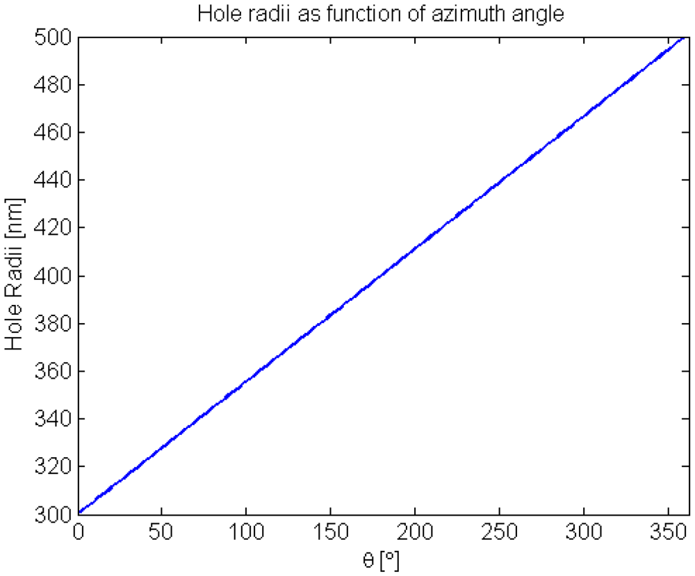
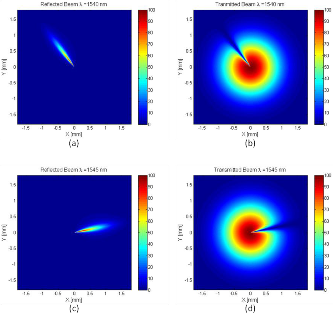
Figure 6 shows the hole radii variation as a function azimuth angle used to generate these simulated beam profiles. The theoretical transmitted and reflected beam profiles for the space variant GMRF shown in
Figure 5 are shown in
Figure 7. The general reflectance profile was determined by assuming a linear change in the hole diameter as a function of the azimuth angle in the plane of the device. The hole size variation limits are the same as in
Figure 4. The incident beam was assumed to be a Gaussian plane wave with a waist of diameter 2.4 mm located, 5.0 cm in front of the GMRF device. From
Figure 7, it can be seen that the reflection profiles are pie wedges of the Gaussian beams, and the transmitted beams have pie wedges removed from them. The transmitted beams appear to change with the azimuth angle only near the resonance location.
Figure 6.
Hole radii variation as a function of azimuth angle.
Figure 6.
Hole radii variation as a function of azimuth angle.
Figure 7.
Simulated Transmission and Reflection Beam profiles. (a) reflected beam for wavelength of 1,540 nm; (b) transmitted beam for wavelength of 1,540 nm; (c) reflected beams for wavelength of 1,545 nm; and (d) transmitted beam for wavelength of 1,545 nm.
Figure 7.
Simulated Transmission and Reflection Beam profiles. (a) reflected beam for wavelength of 1,540 nm; (b) transmitted beam for wavelength of 1,540 nm; (c) reflected beams for wavelength of 1,545 nm; and (d) transmitted beam for wavelength of 1,545 nm.
3. Fabrication Methods
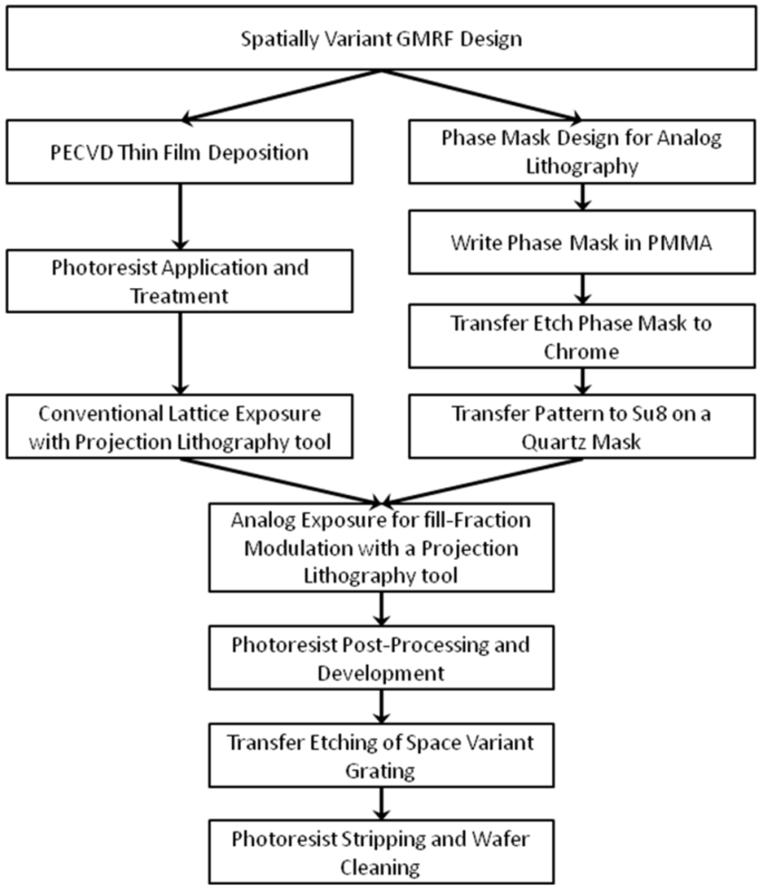
This device was fabricated using processes that are compatible with standard micro-fabrication techniques. The space variant GMRF was created by first depositing the dielectric layers onto a fused silica substrate. Next, the space variant lattice was patterned in photoresist and transfer etched into the silicon oxide layer.
Figure 8 displays the process flow for the fabrication of the device.
The dielectric layers were deposited onto a fused silica substrate using an STS Plasma Enhanced Chemical Vapor Deposition tool. The silicon nitride layer was deposited using Silane (SiH4) and an Ammonia (NH4) gas chemistry. The gas chemistry for the silicon oxide was Silane and Nitrous Oxide (N2O). The silicon nitride and silicon oxide were deposited to thicknesses of 375 nm and 240 nm, respectively.
This azimuthal pattern distribution is accomplished using a novel analog/binary exposure technique with a projection lithography stepper [
6,
17]. A g-line GCA projection stepper was used to pattern the grating lattice as well as the fill fraction variation. A constant fill fraction SWG is first exposed in Shipley S-1805 positive tone photoresist, using a binary amplitude mask. A quadruple exposure method was used to increase the fidelity of the holes patterned [
18]. The fill-fraction variation was achieved via an additional analog exposure. The process of achieving the space variant fill-fraction is further outlined in
Section 3.1.
Figure 8.
Process flow for the Space Variant GMRF Design.
Figure 8.
Process flow for the Space Variant GMRF Design.
The space variant grating in the resist is then transfer etched into the SWG by the use a Plasma-Therm Versaline High Powered Inductively Coupled Plasma Etcher. The recipe used for this process was a mixture of Freon (CHF3) to oxygen (O2). The SWG was etched to a depth of 170 nm.
3.1. Analog Lithography for Fill-Fraction Modulation
Analog lithography is the term applied to the creation of an analog intensity profile in the wafer plane of a photolithographic system [
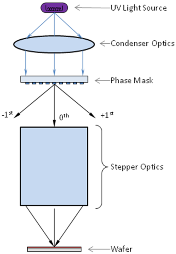
19]. The approach used in this research focuses on the use of a projection lithography system, in this case a GCA 6500 g-line Stepper. An analog intensity profile can be realized using a sub-resolution binary phase grating with a spatially varying fill fraction. The phase grating has a π phase shift to allow full modulation of the intensity profile. When the period of the phase grating is beyond the resolution limit of the projection lithography, the higher diffraction orders will be blocked by the stepper optics. A schematic of this is shown in
Figure 9.
Figure 9.
Schematic drawing of analog lithography.
Figure 9.
Schematic drawing of analog lithography.
The projection system blocks the higher diffraction orders and allows only the 0
th order to propagate, which provides the variation in the intensity of the light incident upon the photoresist as a function of the fill-fraction of the grating. The diffraction efficiency of the 0
th order as a function of fill fraction is given by Equation (1) [
19]. If the fill-fraction of the phase grating is slowly varied across the mask, then the relative intensity of the exposure will also be varied across the device on the wafer. Previous research has shown that this method, of creating an analog intensity profile, can be used to fabricate three dimensional optical elements, as well as, spatially varying the fill fraction or duty cycle of a grating [
17,
19].
![Micromachines 03 00180 i001]()
(1)
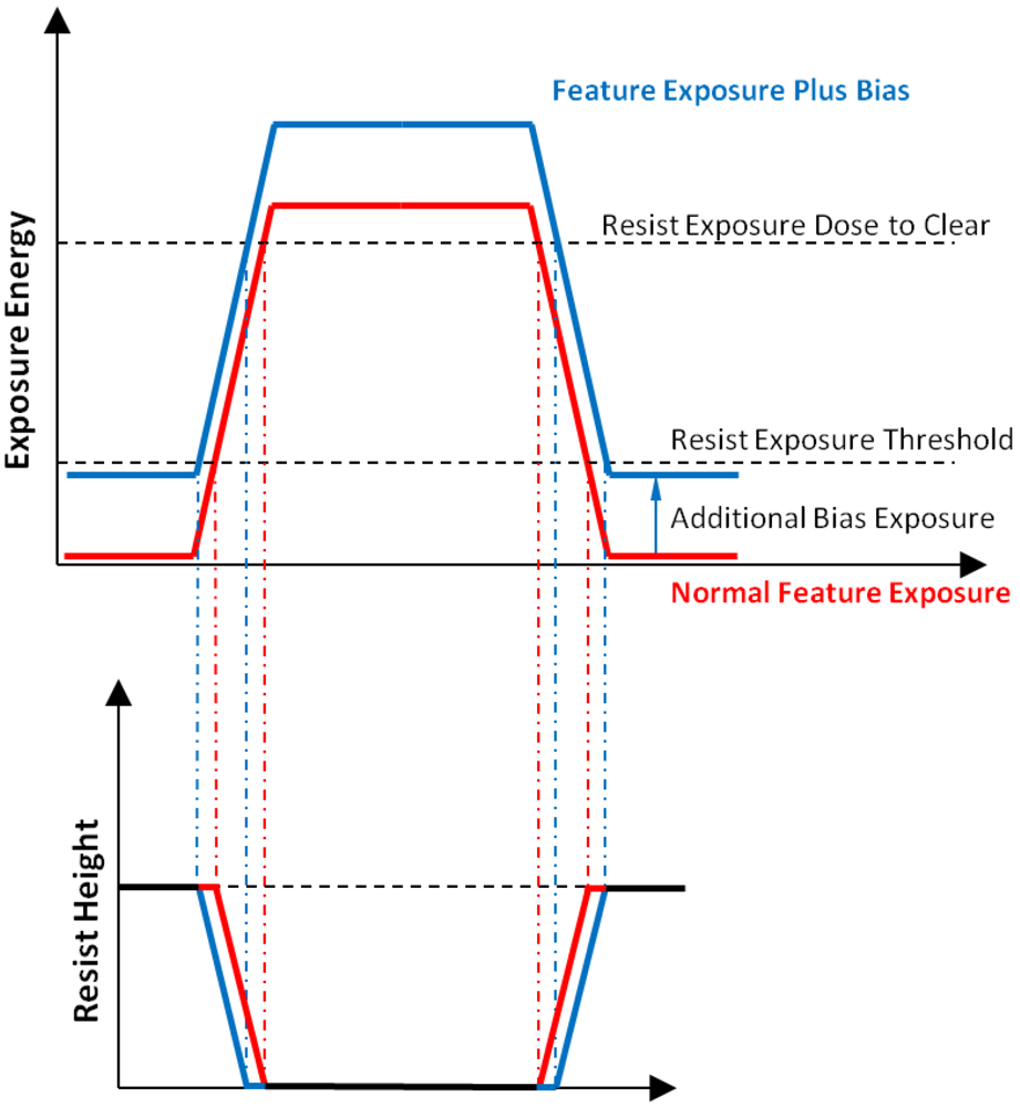
Although a feature near the resolution limit of a projection lithography tool may be exposed with a binary transparent mask, the edges of the feature will be non-vertical; they will be partially exposed. There are two exposure doses relevant to this work. The first is the photoresist’s threshold dose; this is the exposure energy at which point that the photoresist will begin to be removed by the developer. The other exposure dose is called the dose to clear; this is the exposure energy at which the photoresist is completely removed. However, projection lithography systems are not perfect imagers and the edges of a feature will fall between these two doses. If an additional dose is applied to the pattern before it is developed, and that dose is below the threshold of the resist, it will bias the edges of the feature. This will cause the feature width to increase without causing the overall grating pattern to degrade.
Figure 10 depicts a diagram showing this effect. Using analog lithography to apply this relatively small dose, a spatially varying fill fraction in a grating can be achieved.
Figure 10.
Diagram illustrating the principle behind hole size modulation.
Figure 10.
Diagram illustrating the principle behind hole size modulation.
Proprietary software was used to create the mask files for the phase mask used in this work. The phase mask was written in PMMA on a chrome-on-quartz mask using a Leica Electron Beam Pattern Generator 5000. The patterns were then transfer-etched into the chrome layer using a commercial chrome etchant immersion solution. This binary transparent mask was then used to pattern SU8 on a quartz mask. This was done using contact lithography on an i-line Quintel Contact Aligner. The thickness of the SU8 was spun so that it achieved a π phase change for the g-line wavelength of the projection lithography system.
Figure 11 shows the desired analog intensity profile along with a SEM of the center of an azimuthally varying structure using this method.
Figure 11.
(Left) Desired analog intensity; (Right) SEM of an hexagonal grating with an azimuthal fill fraction variation.
Figure 11.
(Left) Desired analog intensity; (Right) SEM of an hexagonal grating with an azimuthal fill fraction variation.
4. Experimental Results and Discussion
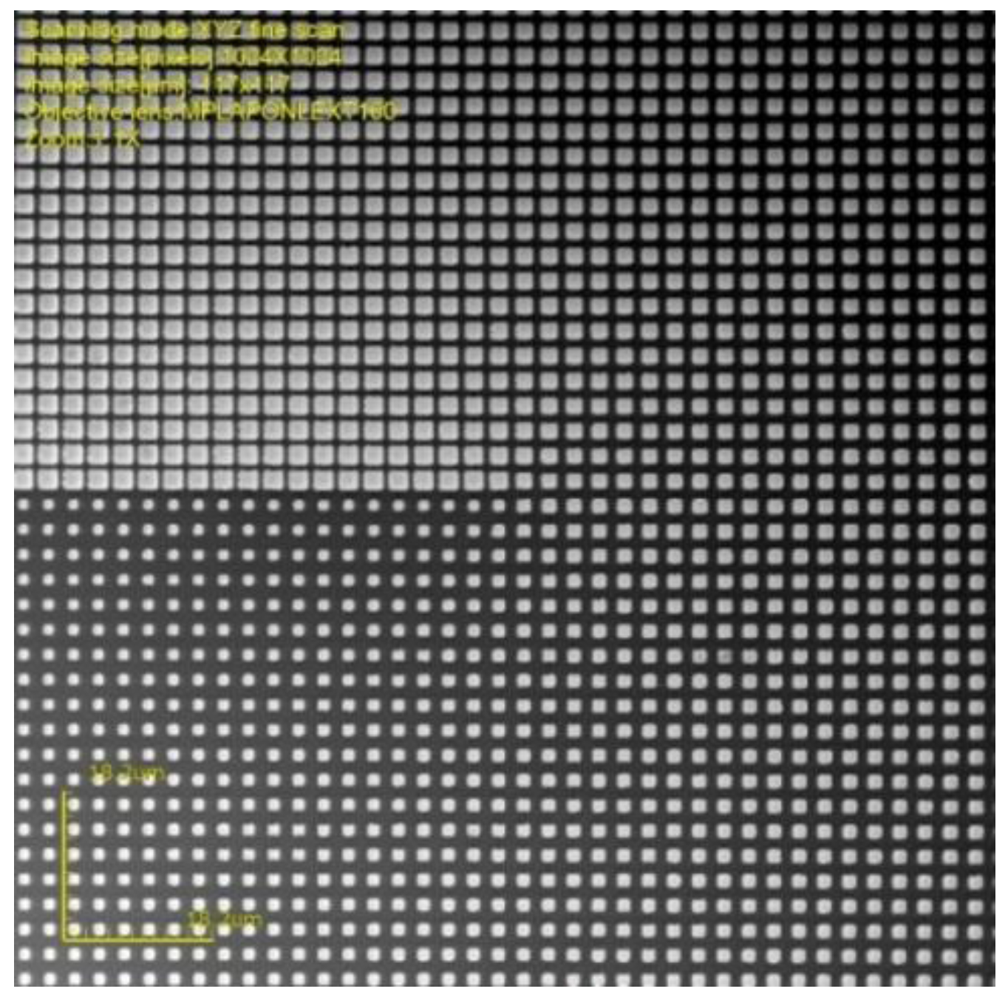
After the phase mask was fabricated, the feature sizes were measured on an Olympus LEXT 3D Confocal Microscope. It was found that during the fabrication procedure, the fill fraction of the phase mask had an additional bias that created a non-linear analog exposure profile.
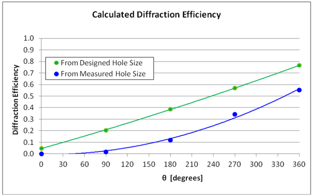
Figure 12 shows an image from the 3D confocal microscope. The square pillars were measured using this microscope at various azimuth angles. These features sizes were used in Equation 1 to create the graph shown in
Figure 13. This graph shows the designed analog intensity profile, analog with the one calculated from measured fill fractions in the phase mask. It shows that the intensity profile should be expected to be non-linear with the azimuth angle.
Figure 12.
Intensity image of the phase mask taking using a Confocal Microscope.
Figure 12.
Intensity image of the phase mask taking using a Confocal Microscope.
Figure 13.
Graph Showing the Diffraction Efficiency of the Phase Mask.
Figure 13.
Graph Showing the Diffraction Efficiency of the Phase Mask.
After the space variant GMRF was fabricated, the hole size variation was measured using a JEOL Scanning Electron Microscope.
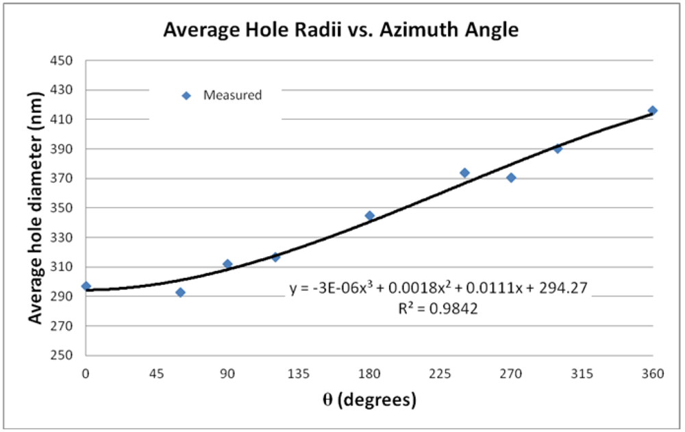
Figure 14 shows a graph demonstrating the spatial variation in hole size. The spatial variation was found to vary non-linearly with azimuth angle. The hole radii ranged from 297 nm to 415 nm. From
Figure 14 and from
Figure 4, we can expect 10.5 nm of resonance shift across 360° of azimuthal angle change.
Figure 14.
Hole radii variation across the device.
Figure 14.
Hole radii variation across the device.
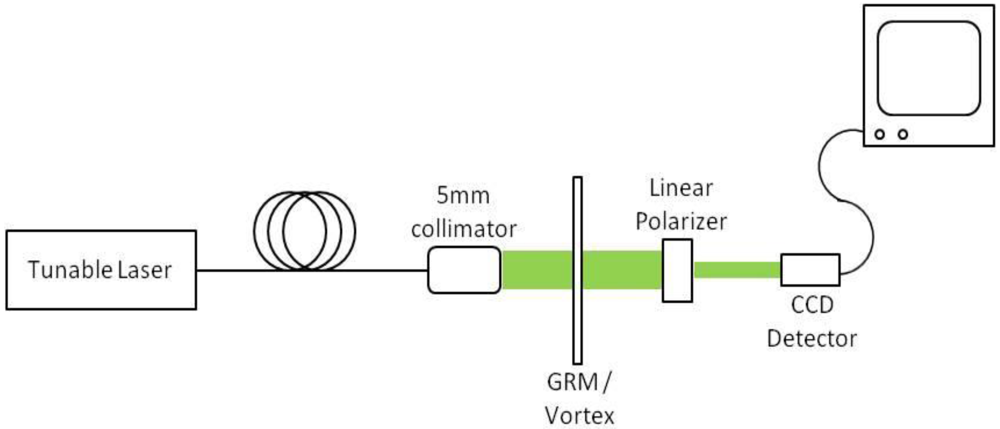
The space variant GMRF’s were interrogated with a fiber tunable laser and a CCD camera. The experimental setup is shown in
Figure 15. An Agilent 8164A Tunable Laser was used as the source for the experimental setup. The source was collimated using an Micro Laser Systems FC5 collimator with an FC connector. A SP-1550 M Spiricon CCD was used to capture images of the transmitted beam. The beam expander and collimator were located 5 cm before the GMRF and the initial beam waist diameter was 2.4 mm.
Figure 15.
Experimental Setup used to test the azimuthally varying GMRF.
Figure 15.
Experimental Setup used to test the azimuthally varying GMRF.
Figure 15 also shows a linear polarizer after the GMRF. During the testing of the GMRF, it was found that the linear polarizer increased the image quality of the transmitted beam. This is most likely due to slight alignment errors during the patterning of the lattice.
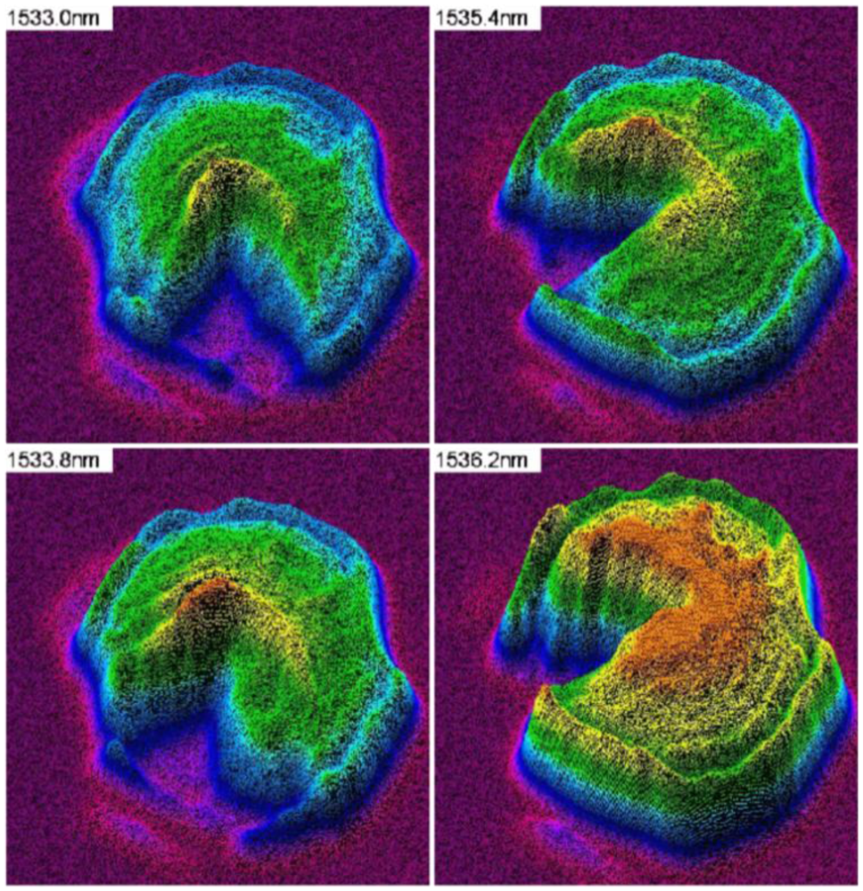
Figure 16 shows the transmitted beam profiles at four different wavelengths: 1,533 nm, 1,535.4 nm, 1,533.8 nm and 1,536.2 nm. From these images we can estimate that the resonance shifts approximately 3.2 nm over a 90° change in azimuth angle, giving the resonance change at 28 degrees/nm. This corresponds to roughly 12 nm of resonance shift for a 360° change in azimuth angle, which is similar to the expected results of 10.5 nm of resonance shift. There was also a noticeable blue shift of approximately 3 nm from the expected results. This could be from slight variations from the designs in the silicon oxide thickness, silicon nitride thickness, and the SWG etch depth. The images shown in
Figure 16 include interference fringes across the beam profiles which are caused by diffraction from the linear polarizer in the setup.
Figure 16.
The transmitted beam profiles at four different wavelengths.
Figure 16.
The transmitted beam profiles at four different wavelengths.

 (1)
(1)