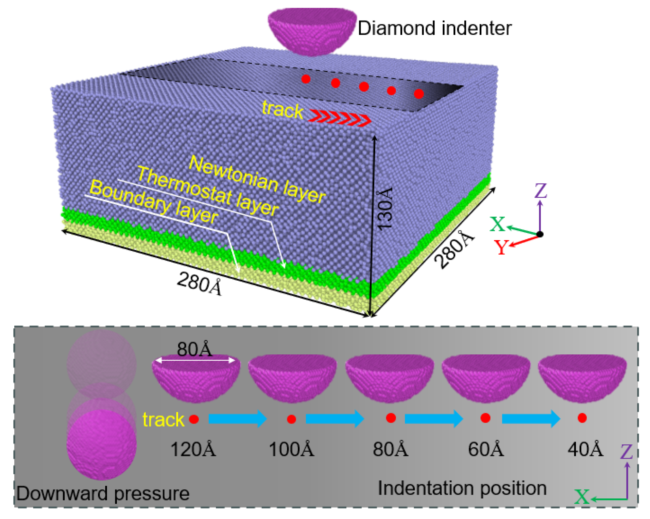
3.1. Surface Deformation Mechanism
During the nanoindentation of single-crystal silicon, the position of the indentation greatly influences the morphology of the indented region.
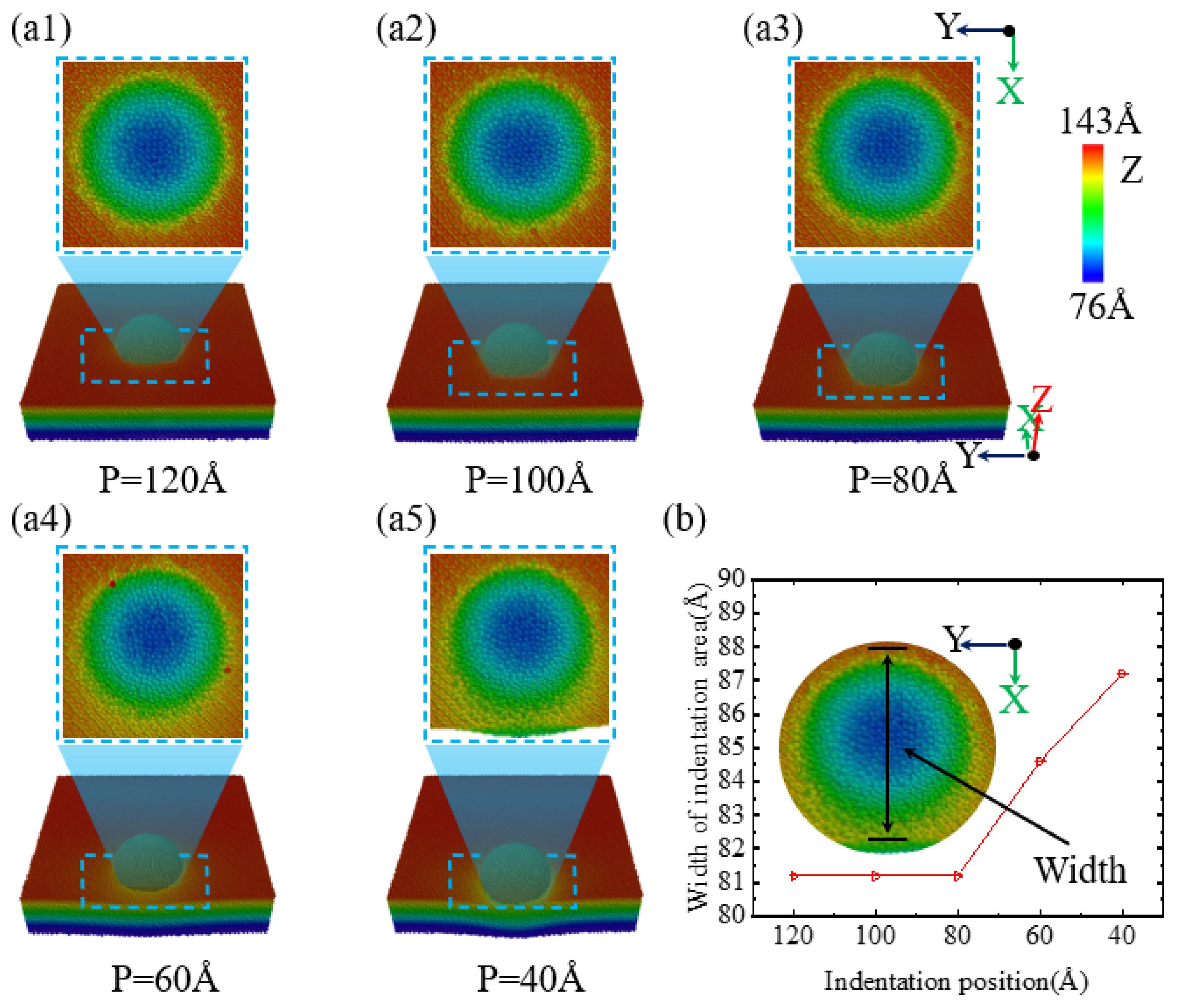
Figure 2(a1–a5) illustrate how the morphology of the indented area changes with varying indentation positions. When the indentation positions are 120 Å, 100 Å, and 80 Å, as shown in
Figure 2(a1–a3),b, the indented area exhibits a circular collapse with a diameter of 80 nm, and the depth of the collapse is generally consistent at 81.25 Å. However, when the indentation position is further moved in the -X direction, that is, towards the edge of the specimen, as illustrated in
Figure 2(a4), at an indentation position of 60 Å, a slight collapse begins to appear along the -X direction at the edge of the indentation, though the collapse depth does not show significant change. As depicted in
Figure 2(a5), a progressive increase in the collapse area along the -X axis is observed at 40 Å as the indentation point approaches the sample’s perimeter. Simultaneously, the collapse depth exhibits a substantial rise. Furthermore,
Figure 2b illustrates that at an indentation depth of 4.6 nm and for positions at or beyond 80 Å, the morphology of the indented area on the specimen surface remains the same. However, when the indentation position is less than or equal to 60 Å, the collapse area of the indentation on the single-crystal silicon specimen surface increases as the indentation position moves closer to the edge of the specimen.
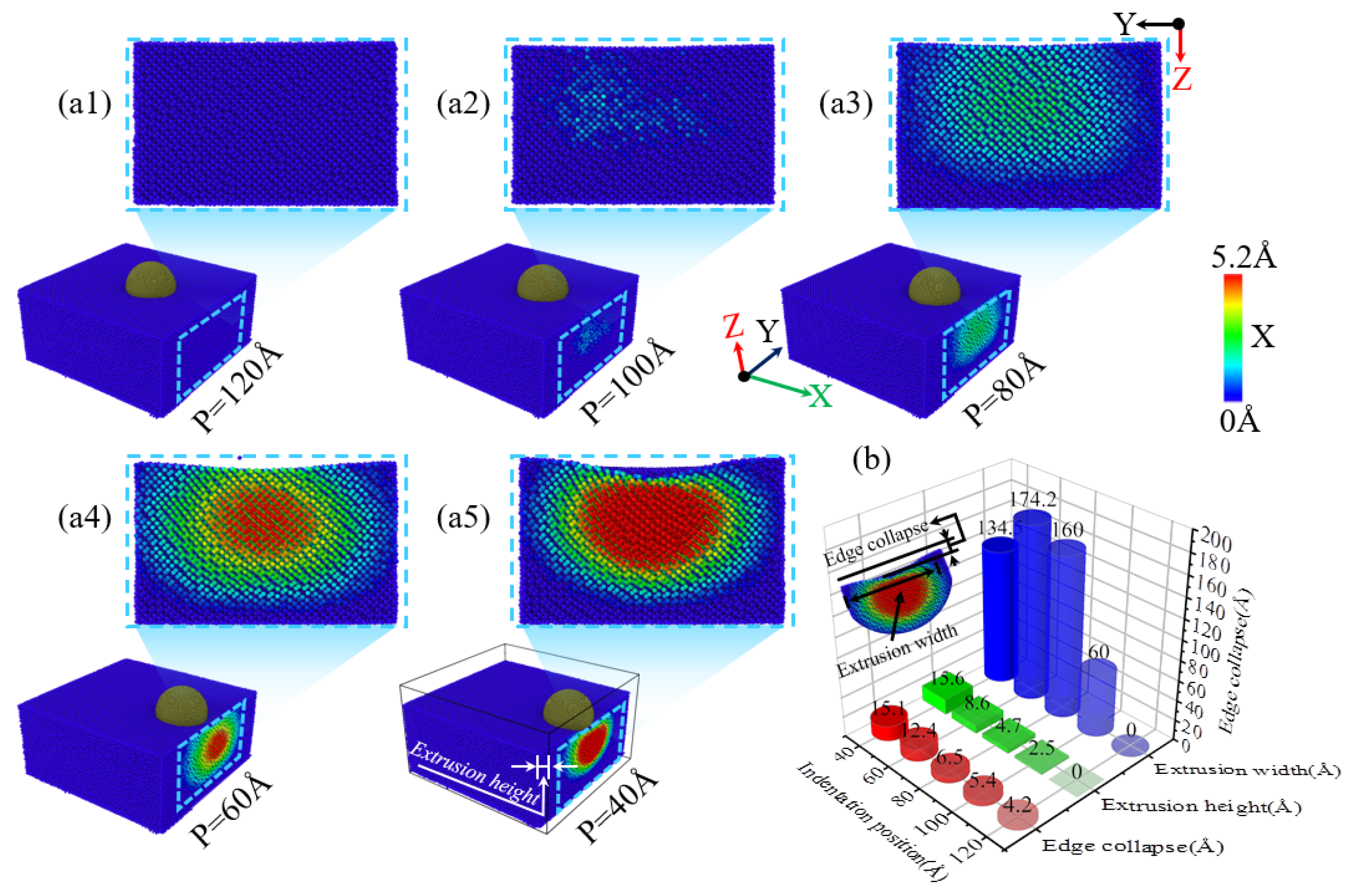
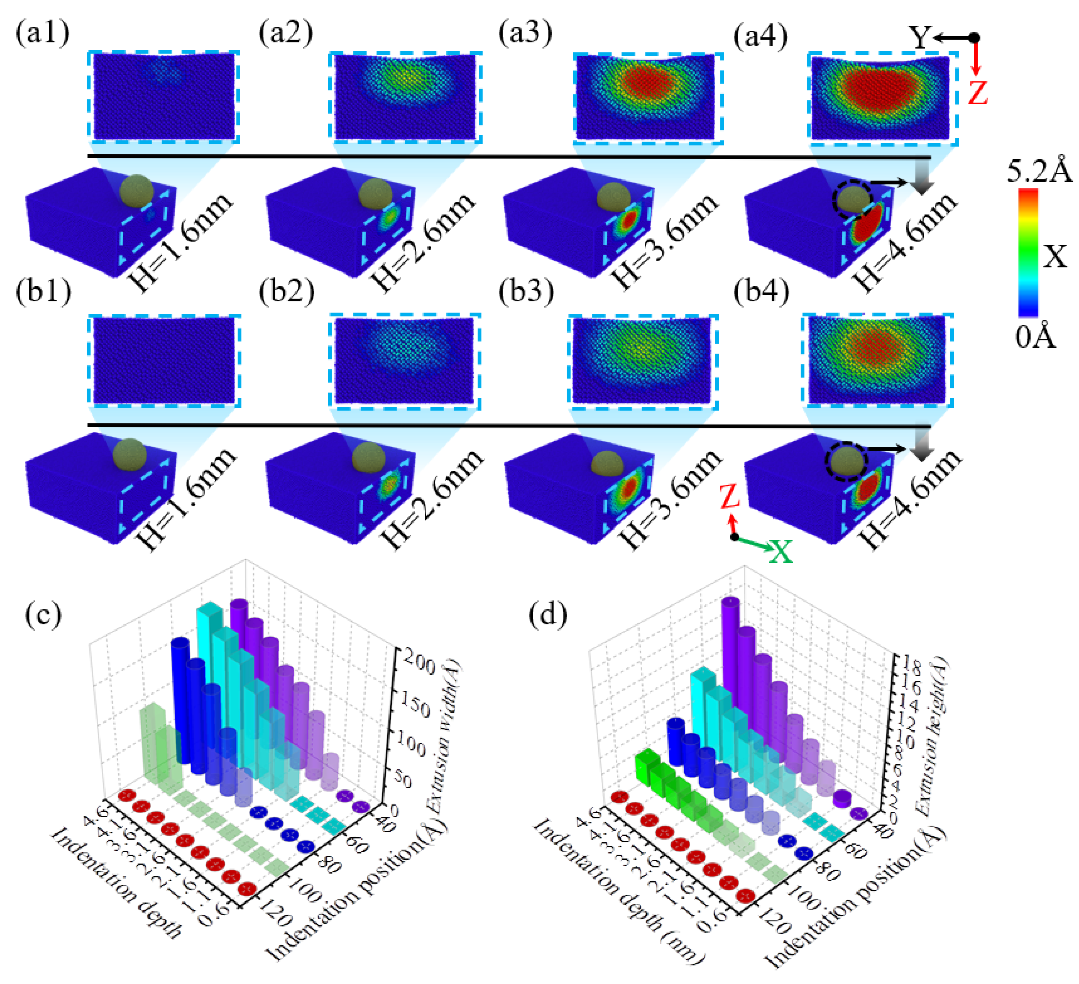
During the nanoindentation of single-crystal silicon using a diamond indenter, the location of the indentation plays a role in the material’s extrusion behavior along the specimen’s edge.
Figure 3(a1–a5) illustrates the resulting extrusion morphologies observed on the single-crystal silicon specimen’s side at a consistent 4.6 nm indentation depth but with varying indentation positions. At a 120 Å indentation position, the specimen’s side maintains its smoothness, and no material extrusion is observed, as depicted in
Figure 3(a1). However, at an indentation position of 100 Å, as shown in
Figure 3(a2), a small amount of slight material extrusion begins to appear. As the indenter moves further towards the -X direction of the specimen edge, as illustrated in
Figure 3(a3), at an indentation position of 80 Å, there is noticeable material extrusion with a larger extrusion area and a significantly increased extrusion height. As the indenter approaches the -X direction edge of the specimen further, as illustrated in
Figure 3(a4),b, as the indentation position moves towards the edge, it can be observed that the width and height of the material extrusion at the edge of the specimen show a gradually increasing trend. However, compared to the indentation position of 80 Å, when the indentation position is 60 Å, as shown in
Figure 3(a4,a5),b, the extrusion area on the specimen’s side decreases while the extrusion height increases significantly as the indenter moves further towards the -X direction of the specimen edge, and the collapse area at the indentation position on the specimen surface also shows an expanding trend. As illustrated in
Figure 3b, with the indentation position moving closer to the -X direction edge of the specimen, the depth of collapse in the edge region increases progressively, with a more significant increase at an indentation position of 60 Å, and the extrusion height also gradually increases, with a more significant increase at 40 Å. Additionally, the change in the width of the material extrusion on the side of the specimen is also closely related to the indentation position. For indentation positions of 120 Å, 100 Å, 80 Å, and 60 Å, as the indentation position approaches the edge region, the width of material extrusion on the side of the specimen shows an increasing trend, but at 40 Å, the width of the material extrusion significantly decreases. In addition, the morphology of the extruded side of the material is elliptical, which is consistent with the simulation results of previous scholars and is caused by the diamond cubic crystal structure of single-crystal silicon [
39].
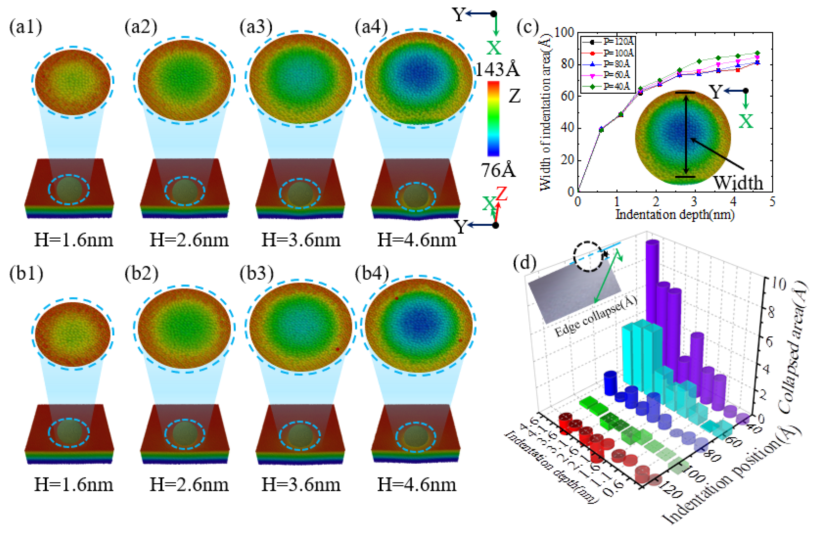
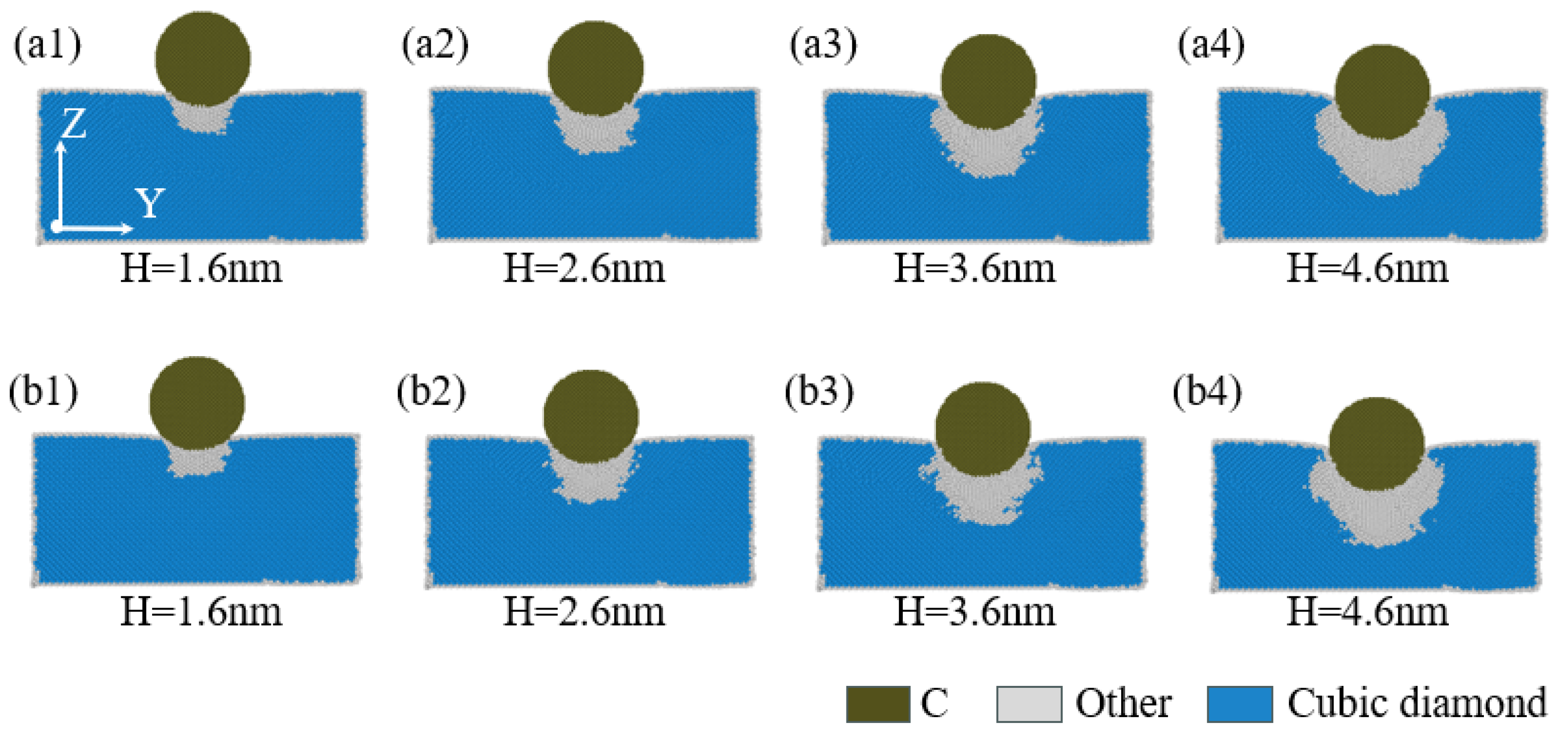
When performing nanoindentation experiments on the edge of single-crystal silicon using a diamond indenter, the experimental results show that the indentation depth has a significant impact on the edge effect. As illustrated in
Figure 4(a1,b1),c, when the indentation depth is 1.6 nm, the indentation area sizes at positions 40 Å and 60 Å are similar. However, when the indentation depth reaches or exceeds 2.6 nm, as illustrated in
Figure 4(a2–a4,b1–b4), as the indentation depth increases, the area of the indented region on the specimen surface also expands accordingly. This is mainly because the indenter is spherical; when the indentation depth is less than the indenter radius, an increase in indentation depth will lead to an increase in the contact area between the specimen and the indenter, resulting in a larger indentation area, consistent with previous research on nickel edge effects [
49]. In addition, at an indentation depth of 4.6 nm, an obvious collapse phenomenon appeared at the edge of the indentation area on the specimen surface.
Figure 4c shows the curve of the indentation area width on the specimen surface as a function of indentation depth for different indentation positions. As illustrated in
Figure 4c, when the indentation depth is no less than 2.6 nm, the indentation area on the specimen surface increases with increasing depth, and at positions 40 Å and 60 Å, the area increase is particularly significant.
Figure 4d shows the variation in the height difference on the specimen surface under different indentation positions and depth conditions. It can be observed that when the indentation position is greater than or equal to 80 Å, the height difference value on the specimen surface is relatively small and exhibits irregularity. However, as the indentation position gradually approaches the edge of the specimen, especially at positions 40 Å and 60 Å, the height difference value on the specimen surface increases significantly, which strongly proves the existence of the edge effect in single-crystal silicon materials.
When performing nanoindentation experiments on the edge of a single-crystal silicon specimen using a diamond indenter, the amount of material extruded from the side of the specimen is modulated by the indentation depth. As illustrated in
Figure 5(a1,b1), when the indentation depth is set to 1.5 nm, no obvious particle extrusion phenomenon is observed at the 80 Å indentation position; in contrast, at the 40 Å position, elliptical material extrusion occurs on the side of the specimen, accompanied by a slight collapse is at the edge in the -X direction. As illustrated in
Figure 5(a2–a4,b2–b4), as the indentation depth increases, the amount of material extruded from the side of the specimen also shows an upward trend. When the indentation position is 60 Å and the depth exceeds 2.6 nm, a small collapse begins to appear at the edge of the indentation in the -X direction, and the width of the material extrusion is significantly higher than at 40 Å, while the height of extrusion is lower at 60 Å compared to 40 Å. At indentation depths greater than 2.6 nm, the collapse range and height at the -X direction edge of the indentation at 60 Å are also lower compared to 40 Å.
Figure 5c,d present bar charts showing the variation in the width and height of material extrusion on the specimen side with different indentation depths and positions. When the indentation position is 120 Å, based on the results presented in
Figure 5c,d, no material extrusion is observed at different indentation depths, indicating that edge effects are not present at this position. However, at indentation positions of 100 Å, 80 Å, 60 Å, and 40 Å, distinct differences in material extrusion on the specimen side are evident. As illustrated in
Figure 5c,d, as the indentation position gradually approaches the edge of the specimen in the -X direction, the material extrusion phenomenon begins to appear at smaller indentation depths; moreover, both the width and height of the material extrusion increase with the increase in the indentation depth, which, in turn, leads to a more and more obvious edge effect.
3.2. Mechanical Properties
Figure 6a depicts the fluctuation in the number of material extrusion particles on the side of the specimen with indentation depth at different indentation positions;
Figure 6b further elucidates the critical indentation depth at which material extrusion begins to appear on the side of the specimen at various indentation positions. According to
Figure 6b, when the indentation position is set to 120 Å, no particle extrusion is observed on the specimen side, indicating that no edge effects are present at this indentation position. However, when the indentation position is 100 Å and the indentation depth is 3.6 nm, material extrusion begins to appear on the specimen side, indicating that slight edge effects start to emerge in the single-crystal silicon specimen at this point. Additionally, as the indentation position moves closer to the specimen edge, according to
Figure 6a, the number of extrusion particles on the side of the specimen increases significantly, exhibiting a linear increasing trend for indentation positions less than 60 Å, indicating a clear edge effect. For indentation positions less than 100 Å, under the same indentation depth conditions, the number of extrusion particles on the side of the specimen significantly increases as the indentation position approaches the edge. When the indentation depth is below 1.1 nm, no particle extrusion is observed on the specimen side for different indentation positions. Furthermore, according to
Figure 6b, as the indentation position gradually approaches the edge of the specimen, the depth at which material extrusion begins to occur on the side of the specimen also gradually decreases.
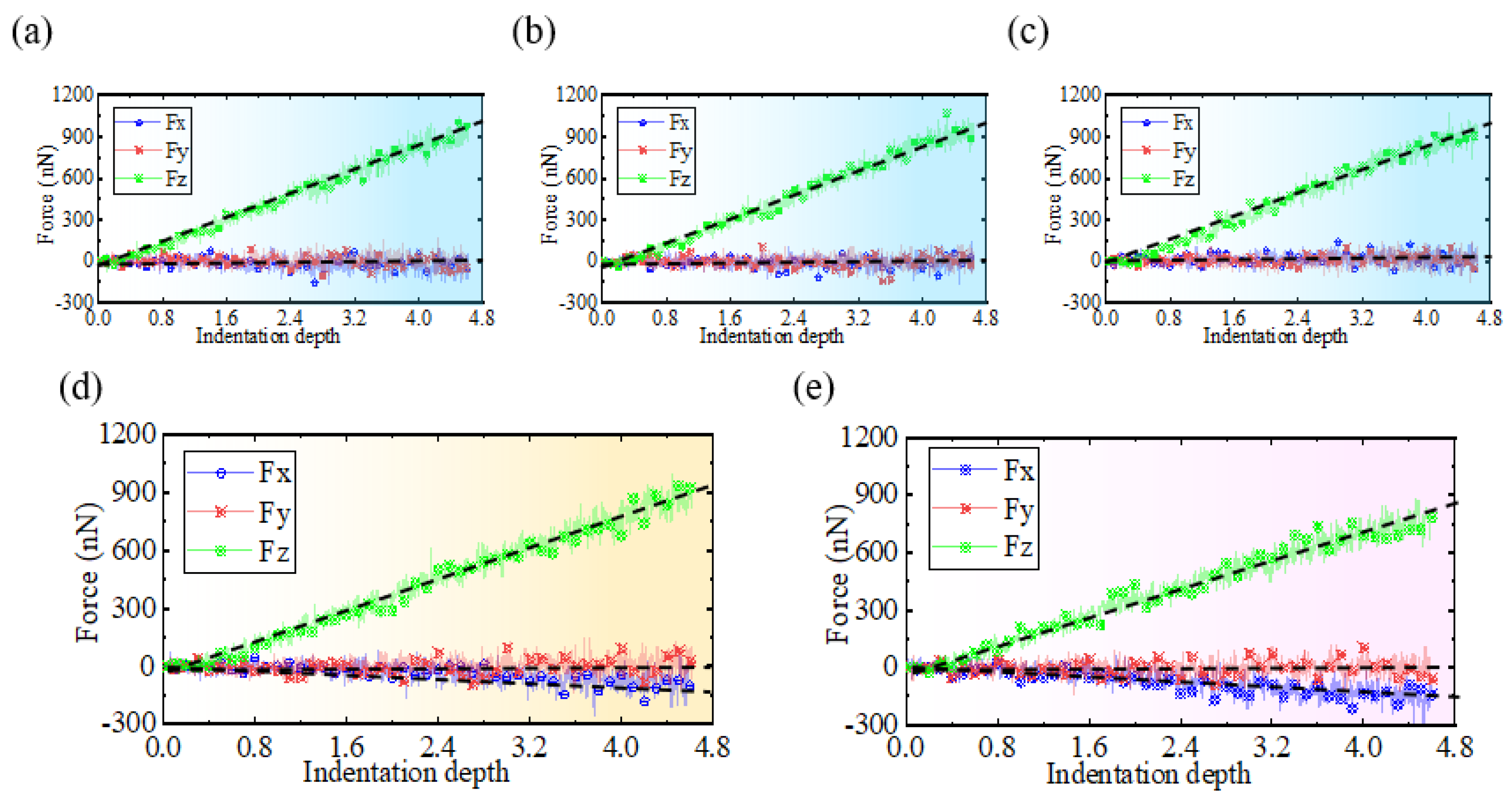
When performing nanoindentation experiments on the edge of single-crystal silicon using a diamond indenter, both the indentation depth and position exert a modulating effect on the indentation force.
Figure 7a–e visually represent the trend of the indentation force changing with indentation depth at different indentation positions. As illustrated in
Figure 7a–c, when the indentation position exceeds 80 Å, the vertical indentation force Fz exhibits a linear increasing trend with the increase in indentation depth, and when the indentation depth reaches 4.6 nm, its peak force value approaches 1050 nN, while the horizontal indentation forces
Fx and
Fy show no significant trend, fluctuating around zero and remaining stable. However, when the indentation position is less than or equal to 60 Å, as illustrated in
Figure 7d,e,
Fz starts to exhibit variations. The rate of the increase in Fz decreases as the indentation position moves closer to the specimen edge. Under the maximum indentation depth condition of 4.6 nm, the peak force values of
Fz corresponding to the indentation positions of 80 Å and 60 Å are approximately 920 nN and 880 nN, respectively. Concurrently, the horizontal indentation force Fx also begins to exhibit an increasing trend along the negative X direction, with its peak force value being approximately −150 nN. At an indentation position of 40 Å, the fluctuation in
Fx becomes more pronounced. For
Fy, when the indentation position is less than 60 Å, the force remains around zero with a slight increase in fluctuation amplitude.
Figure 8 shows the changes in the average hardness and variance in single-crystal silicon at different indentation positions. As the indentation position gradually approaches the edge, the average hardness of the silicon decreases, indicating that the hardness of the material at the edge is low, which is also the reason for the decrease in the indentation force
Fz. At the same time, regarding the variance in the hardness of single-crystal silicon, the magnitude of the change in material hardness changes with the depth of indentation. It can be seen that the hardness variance is highest at the indentation position of 100 Å and then gradually decreases to reach its minimum value at 40 Å, indicating that the hardness change in the material at 100 Å is relatively large, while the hardness change at the edge position is relatively small with the depth of indentation.
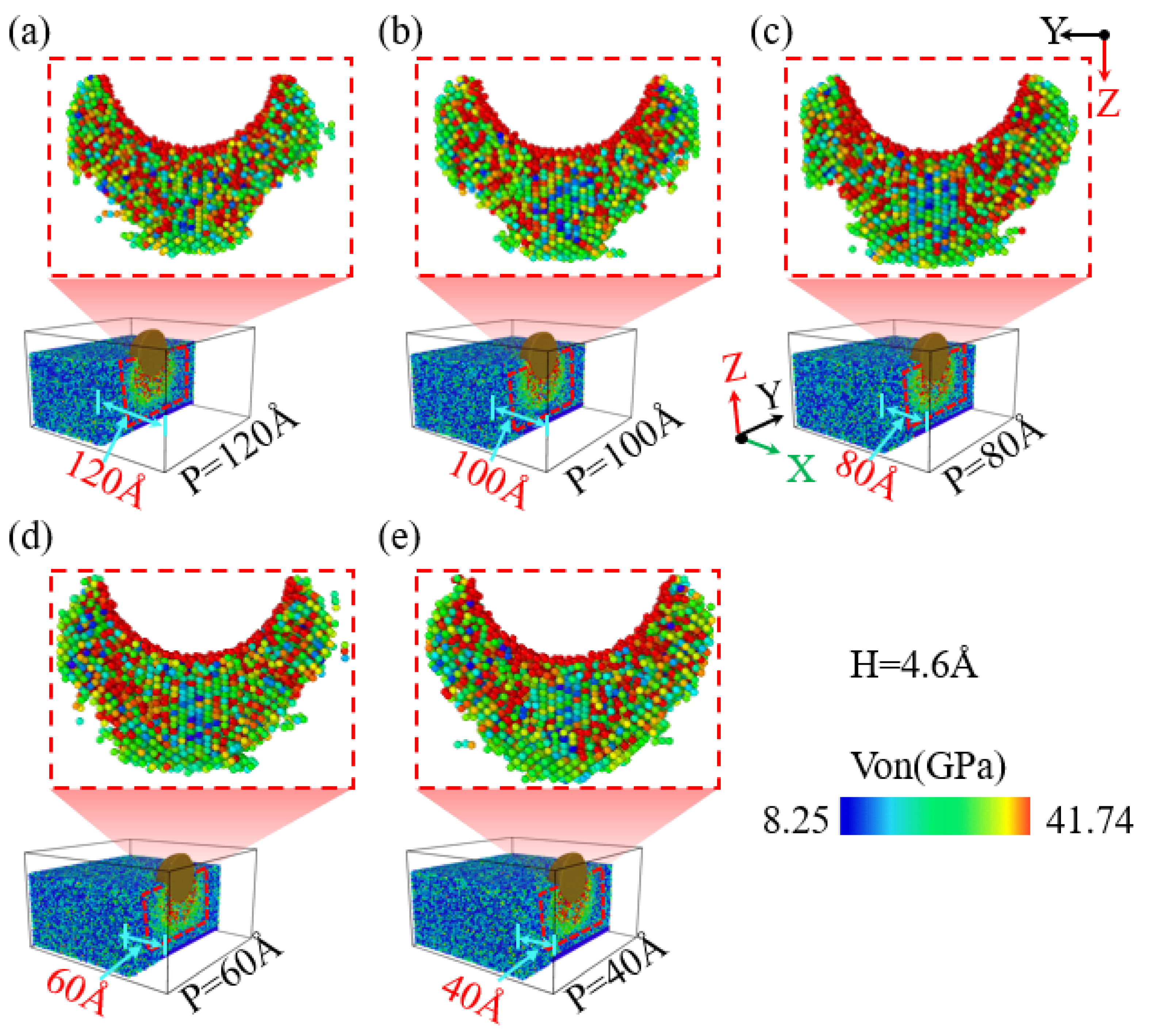
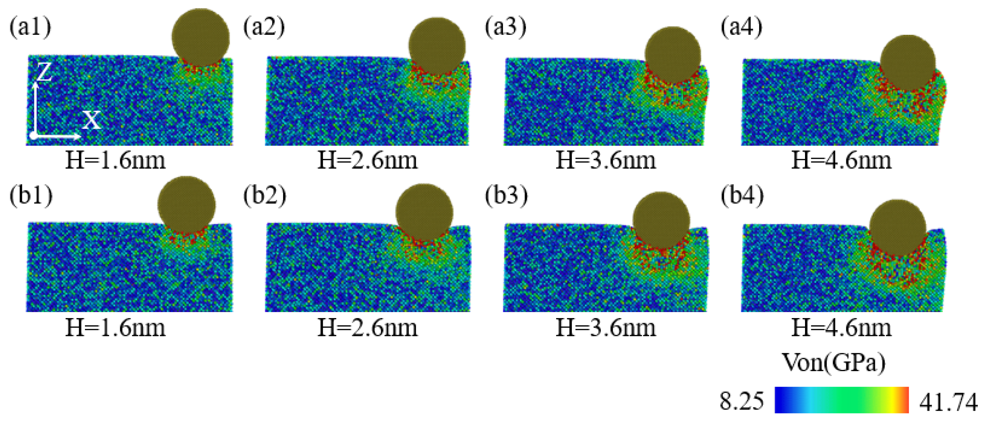
When performing nanoindentation experiments on the edge of single-crystal silicon using a diamond indenter, the indentation position significantly modulates the stress field distribution beneath the indenter.
Figure 9a–e depict, in schematic diagram form, the influence of different indentation positions on the stress field distribution within the YZ plane of the specimen at an indentation depth of 4.6 nm. As illustrated in
Figure 9a–c, when the indentation positions are 120 Å, 100 Å, and 80 Å, the distribution pattern of the stress beneath the indenter within the YZ plane is primarily concentrated directly beneath the indenter and on either side, and the distribution is relatively symmetrical. However, contrasting
Figure 9d,e, it can be observed that as the indentation position approaches the edge of the specimen, at positions such as 60 Å and 40 Å, the distribution pattern of stress beneath the indenter within the YZ plane begins to shift towards the Y direction of the specimen. The high-stress regions also shift accordingly, with the distribution of high-stress areas becoming concentrated more in the Y direction beneath the indenter in the YZ plane. Additionally, referencing
Figure 9a–e, it is evident that as the indentation position gradually approaches the edge of the specimen, both the range and depth of the stress distribution beneath the indenter within the YZ plane increase, while simultaneously, the depth of the high-stress region exhibits a progressively decreasing trend, this indicates that the phenomenon of edge stress concentration is consistent with the changes in the surface collapse morphology of the material. In addition, it can be observed that the stress does not propagate to the bottom of the material, and the fixed substrate is not affected by indentation. The simulation results are reliable.
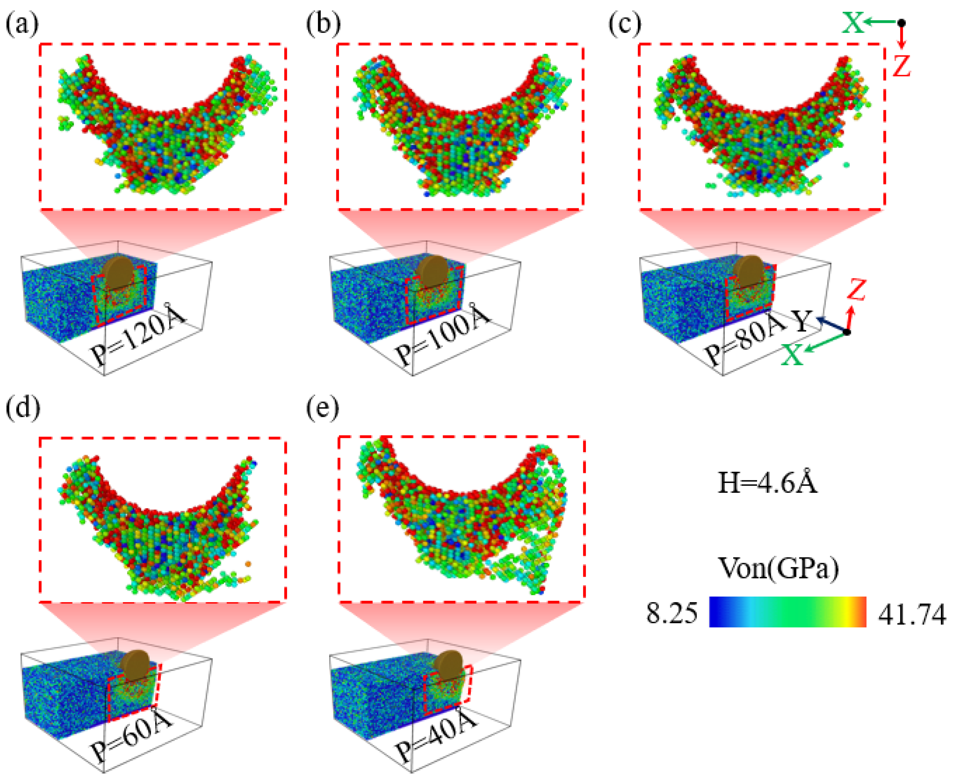
Figure 10 shows the stress distribution within the XZ plane of the specimen at an indentation depth of 4.6 nm for different indentation positions. According to
Figure 10a, when the indentation position is set to 120 Å, the high-stress region beneath the indenter in the XZ plane is mainly gathered directly below the indenter. However, contrasting
Figure 10b,c, it can be observed that as the indentation position approaches the edge of the specimen, at positions of 100 Å and 80 Å, the high-stress region distribution in the XZ plane beneath the indenter begins to shift towards the -X direction of the specimen. Despite this shift, the high-stress areas are still mainly concentrated beneath the indenter and on either side, maintaining a relatively symmetrical distribution. As illustrated in
Figure 10d,e, with further movement of the indentation position towards the edge of the specimen, at positions of 60 Å and 40 Å, the high-stress region beneath the indenter in the XZ plane shows a significant increase in the shift towards the -X direction, this is consistent with the trend of material side extrusion changing with the indentation position. The distribution of the stress region becomes primarily concentrated in the -X direction beneath the indenter. Additionally, at an indentation position of 40 Å, the stress beneath the indenter in the XZ plane decreases, simultaneously, the proportional share of the stress region distribution in the -X direction exhibits a significantly increasing trend.
When performing nanoindentation experiments on the edge of single-crystal silicon using a diamond indenter, the indentation depth exerts a crucial impact on the internal stress field distribution of the specimen.
Figure 11(a1–a4,b1–b4) aim to illustrate the pattern of changes exhibited by the stress field distribution within the YZ plane of the specimen with indentation depth, specifically for indentation positions of 40 Å and 60 Å. As illustrated in
Figure 11(a1,a2,b1,b2), when the indentation depth is less than or equal to 2.6 nm, the stress distribution and high-stress regions within the YZ plane are mainly concentrated directly beneath the indenter, with the stress distribution being symmetrical relative to the XZ plane. When the indentation depth is greater than or equal to 3.6 nm, as illustrated in
Figure 11(a3,a4,b3,b4), the stress distribution within the YZ plane increases significantly with the indentation depth. The stress field distribution pattern and high-stress regions extend and distribute beneath the indenter and to both lateral sides, with the proportional share of stress regions being more pronounced in the -Y direction compared to the -X direction. Additionally, as illustrated in
Figure 11(a4,b4), under an indentation depth of 4.6 nm, it is observed that the high-stress region distribution within the YZ plane shifts slightly more in the -Y direction for an indentation position of 40 Å compared to the distribution at 60 Å, with the distribution range being deeper.
Figure 12(a1–a4,b1–b4) aim to reveal the pattern of stress variation within the XZ plane of the specimen with indentation depth at indentation positions of 40 Å and 60 Å. Given an indentation depth of 1.6 nm, comparing
Figure 12(a1,b1), it is evident that the stress field distribution pattern and high-stress regions within the XZ plane are mainly concentrated in the area directly beneath the indenter. As the indentation depth continuously increases, referring to
Figure 1(a2–a4,b2–b4), for indentation positions of 40 Å and 60 Å, the stress level within the XZ plane also progressively rises, and the extent of the high-stress regions also expands accordingly. The high-stress regions are mainly concentrated directly beneath the indenter. Considering the influence of the specimen’s lateral face, the stress field distribution in the XZ plane exhibits a tendency to deviate towards the indenter’s -X direction. Additionally, as illustrated in
Figure 12(a1–a4,b1–b4), when the indentation depth is less than or equal to 2.6 nm, the stress distribution within the XZ plane at indentation positions of 40 Å and 60 Å is essentially similar. However, when the indentation depth is no less than 3.6 nm, the stress distribution and extent of the high-stress regions within the XZ plane beneath the indenter for an indentation position of 60 Å are significantly greater compared to those for an indentation position of 40 Å.
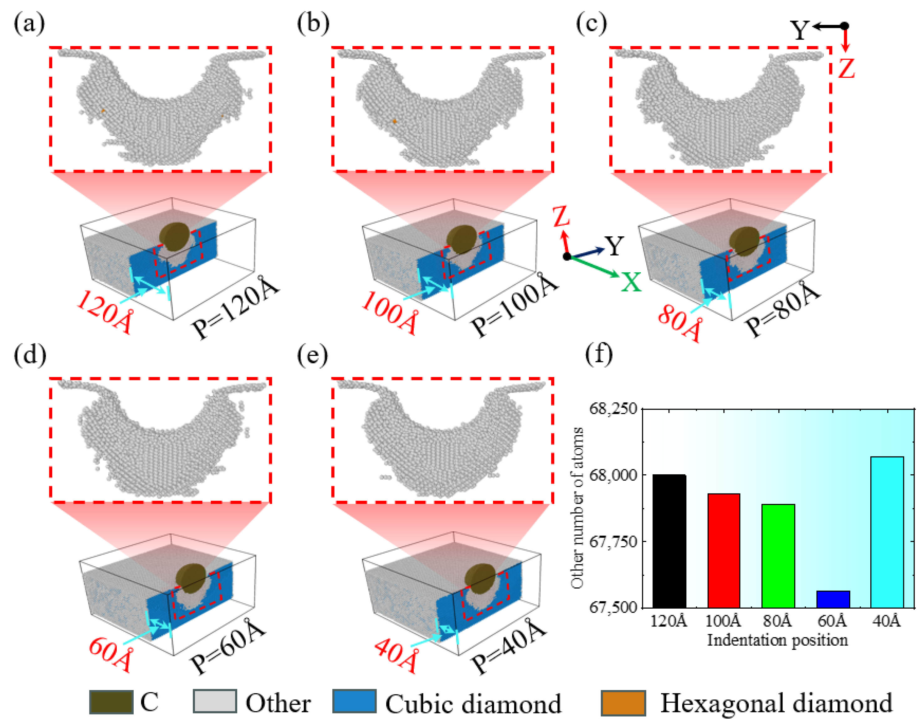
3.3. Internal Phase Transition
When conducting nanoindentation experiments on the edge of single-crystal silicon using a diamond indenter, the indentation position influences the phase transformation phenomenon beneath the indenter.
Figure 13a–e present, in the form of schematic diagrams, the characteristics of the phase transformation regions beneath the indenter in the YZ plane at an indentation depth of 4.6 nm for different indentation positions. The reason for the formation of this phase transition is that irreversible plastic deformation occurs at the material edge after nanoindentation, leading to the formation of an amorphous structure inside [
50]. By comparing
Figure 13a,b, it is evident that when the indentation positions are 120 Å and 100 Å, respectively, the distribution range and depth of the phase transformation region beneath the indenter in the YZ plane exhibit a high degree of similarity, primarily concentrated beneath and on either side of the indenter, with a small amount of hexagonal diamond structure observable at the edges of the phase transformation region. However, comparing
Figure 13c–e, it is evident that as the indentation position moves closer to the specimen edge, at 80 Å, differences in the phase transformation region within the YZ plane become evident. Both the range and depth of the phase transformation region are expanded, with the distribution becoming more concentrated directly beneath the indenter and expanding further towards the edge accompanying the indentation position nearing the specimen boundary. Additionally, for different indentation positions, referencing
Figure 13a–e, it is evident that the phase transformation regions beneath the indenter in the YZ plane exhibit a symmetrical distribution pattern with respect to the XZ plane. In addition, it can be observed that the phase transition does not propagate to the bottom of the material, and the fixed substrate is not affected by indentation. The simulation results are reliable. As shown in
Figure 13f, as the indentation position gradually approaches the edge, the number of amorphous particles gradually decreases. However, when the indentation position is 40 Å, the number of amorphous particles suddenly increases. This indicates that during the process of the indentation head gradually approaching the edge, energy is mainly released by ordered phase transition, and the number of amorphous particles decreases. However, when it reaches the outermost position, the material boundary constraint collapses, and the amorphous phase dominates the deformation mechanism.
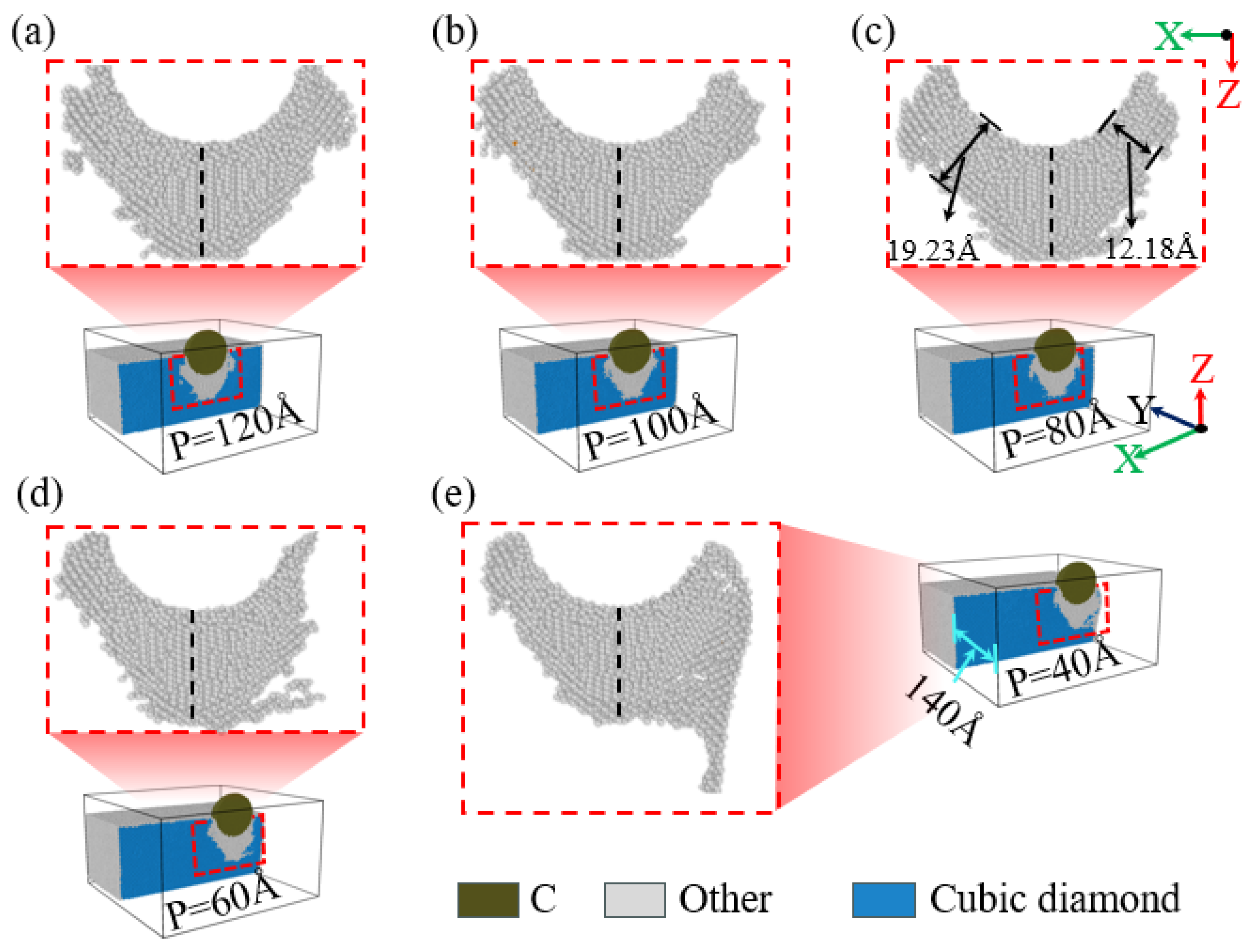
Figure 14a–e show schematic diagrams of the phase transformation regions beneath the indenter in the XZ plane at an indentation depth of 4.6 nm for different indentation positions. Referring to
Figure 14a,b, when the indentation positions are set to 120 Å and 100 Å, the distribution range and depth of the phase transformation region beneath the indenter in the XZ plane exhibit similarity, and both are mainly concentrated beneath the indenter, further manifesting a symmetrical distribution characteristic relative to the YZ plane. However, when the indentation position is 80 Å, as illustrated in
Figure 14c, the distribution of the phase transformation region in the XZ plane starts to expand towards the X direction inside the specimen. Both the distribution range and depth of the phase transformation region are expanded, and slight asymmetry relative to the YZ plane also begins to manifest itself. In contrast, as illustrated in
Figure 14d, when the indentation position moves closer to the specimen edge and is at 60 Å, the distribution of the phase transformation region in the XZ plane starts to extend towards the outer -X direction of the specimen and presents an irregular distribution, this trend indicates that the stacking behavior of side materials is influenced by phase transitions. Additionally, as illustrated in
Figure 14e, when the indentation position is set to 40 Å, the main distribution direction of the phase transformation region beneath the indenter in the XZ plane is concentrated in the -X axial direction, and the distribution range also exhibits a significantly expanded state. However, the depth of the phase transformation region tends to become shallower, and its distribution pattern also exhibits significant asymmetry relative to the YZ plane.
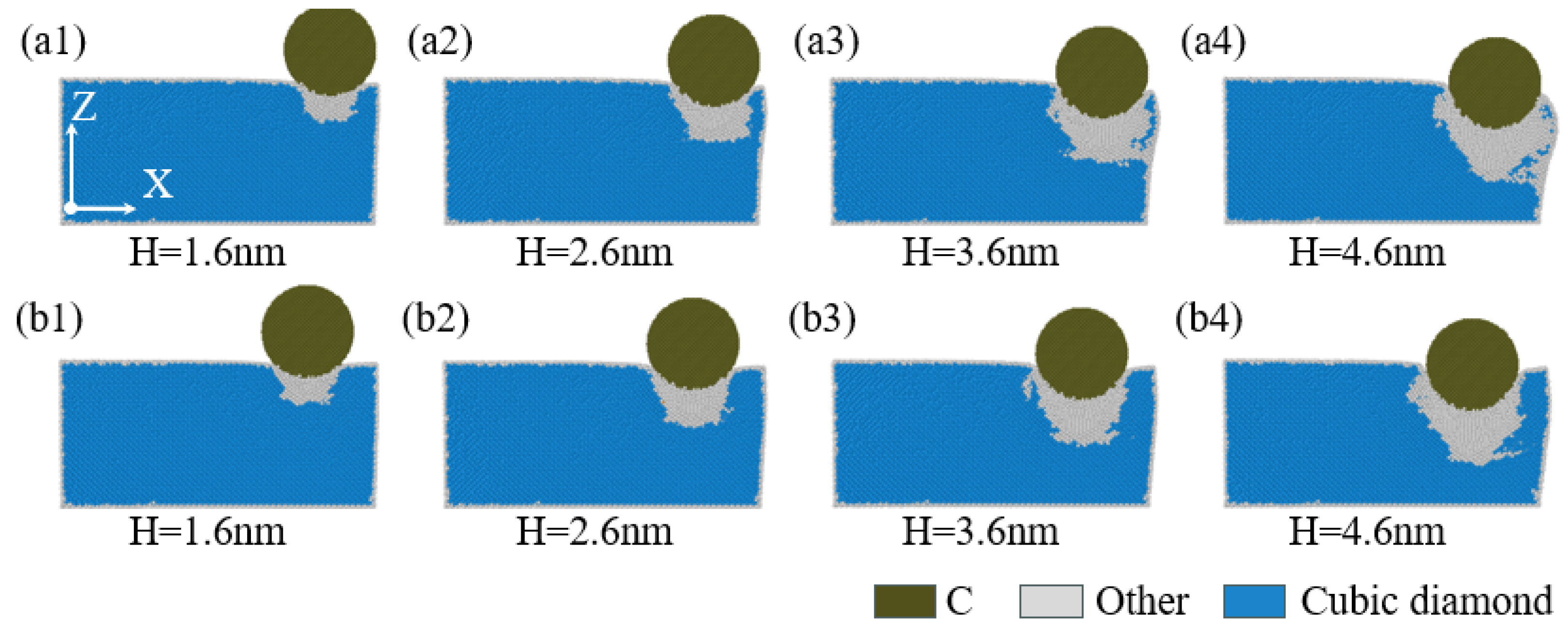
When performing nanoindentation experiments on the edge of single-crystal silicon using a diamond indenter, the indentation depth exerts an action effect on the phase transformation phenomenon beneath the indenter contact area. Referencing
Figure 15(a1,b1), it is evident that at an indentation depth of 1.6 nm, and under indentation positions set at 40 Å and 60 Å, respectively, the distribution pattern of the phase transformation region beneath the indenter in the YZ plane is similar, with the phase transformation area being relatively small and primarily concentrated directly beneath the indenter. As the indentation depth continues to increase, as depicted in
Figure 15(a2,b2), when the depth reaches 2.6 nm, the distribution range of the phase transformation region beneath the indenter in the YZ plane also exhibits a significant expansion with further indentation deepening. At the 40 Å indentation position, a slight displacement of the phase transformation region along the -Y direction exists. However, with further progressive increases in indentation depth, comparing
Figure 15(a3,a4,b3,b4), it is evident that when the depth is no less than 3.6 nm, the distribution range of the phase transformation region in the YZ plane then exhibits a clear expansion. The phase transformation region then begins to gather directly beneath the indenter and on both sides, and the distribution of the phase transformation region also exhibits a pattern approximately symmetrical with the XZ plane.
Figure 16(a1–a4,b1–b4) show schematic diagrams of the phase transformation regions beneath the indenter in the XZ plane at indentation positions of 40 Å and 60 Å as a function of indentation depth. As illustrated in
Figure 16(a1,b1), at an indentation depth of 1.6 nm, the phase transformation regions beneath the indenter in the XZ plane at both 40 Å and 60 Å are similar, with a relatively small distribution range and the phase transformation region concentrated directly beneath the indenter, symmetrically distributed relative to the YZ plane. However, when the indentation depth reaches 2.6 nm, comparing
Figure 16(a2,b2), it is evident that both the distribution range and depth of the phase transformation region beneath the indenter in the XZ plane are expanded, and their distribution pattern also begins to shift towards the -X direction of the specimen. This shift causes slight asymmetry relative to the YZ plane. Accompanying the subsequent increase in indentation depth, referring to
Figure 16(a3,a4,b3,b4), when the depth is no less than 3.6 nm, for both 40 Å and 60 Å indentation positions, the distribution range and depth of the phase transformation region beneath the indenter in the XZ plane both achieve significant enhancement. At larger indentation depths, the shift of the distribution of the phase transformation region in the XZ plane towards the -X direction becomes increasingly pronounced, and this region mainly converges beneath the indenter and tends towards the boundary edge of the specimen in the -X direction, thereby exhibiting an asymmetry characteristic relative to the YZ plane.


