


Simulation Study on 6.5 kV SiC Trench Gate p-Channel Superjunction Insulated Gate Bipolar Transistor


Abstract
1. Introduction
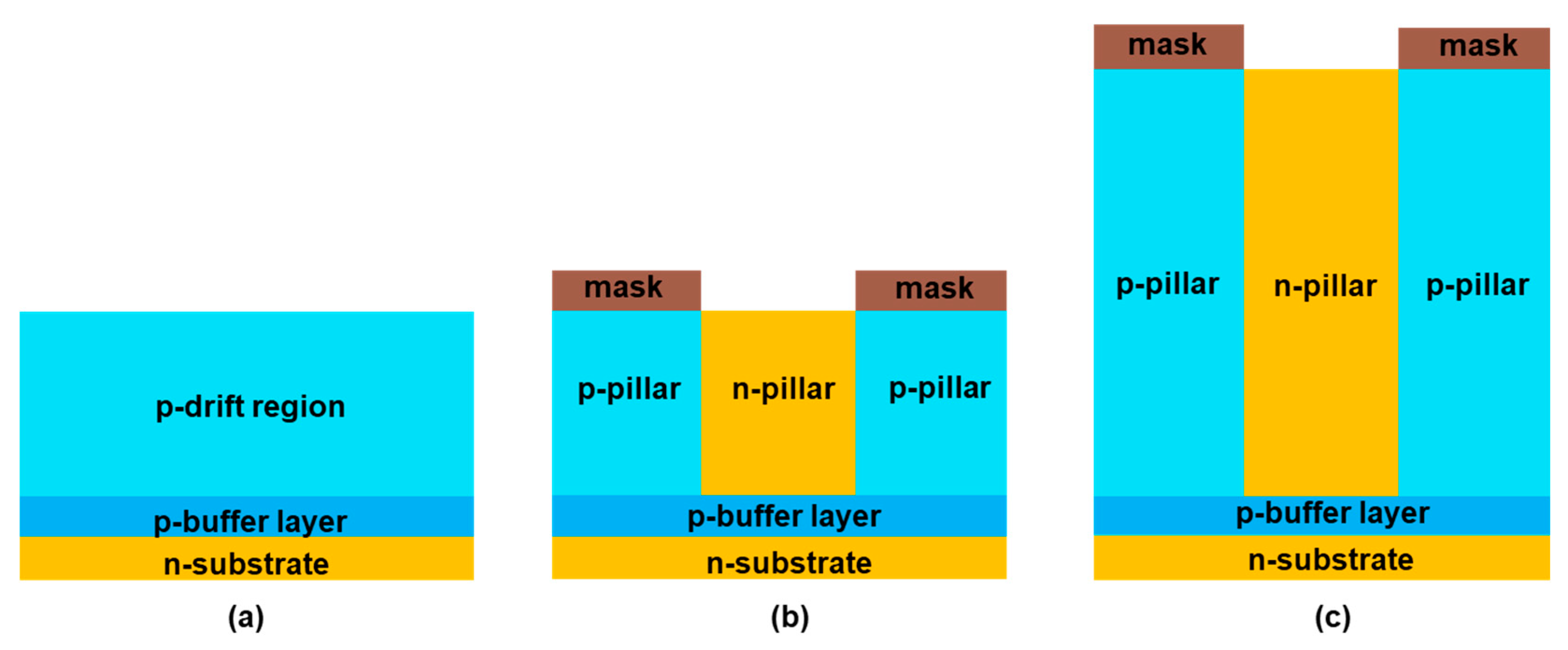
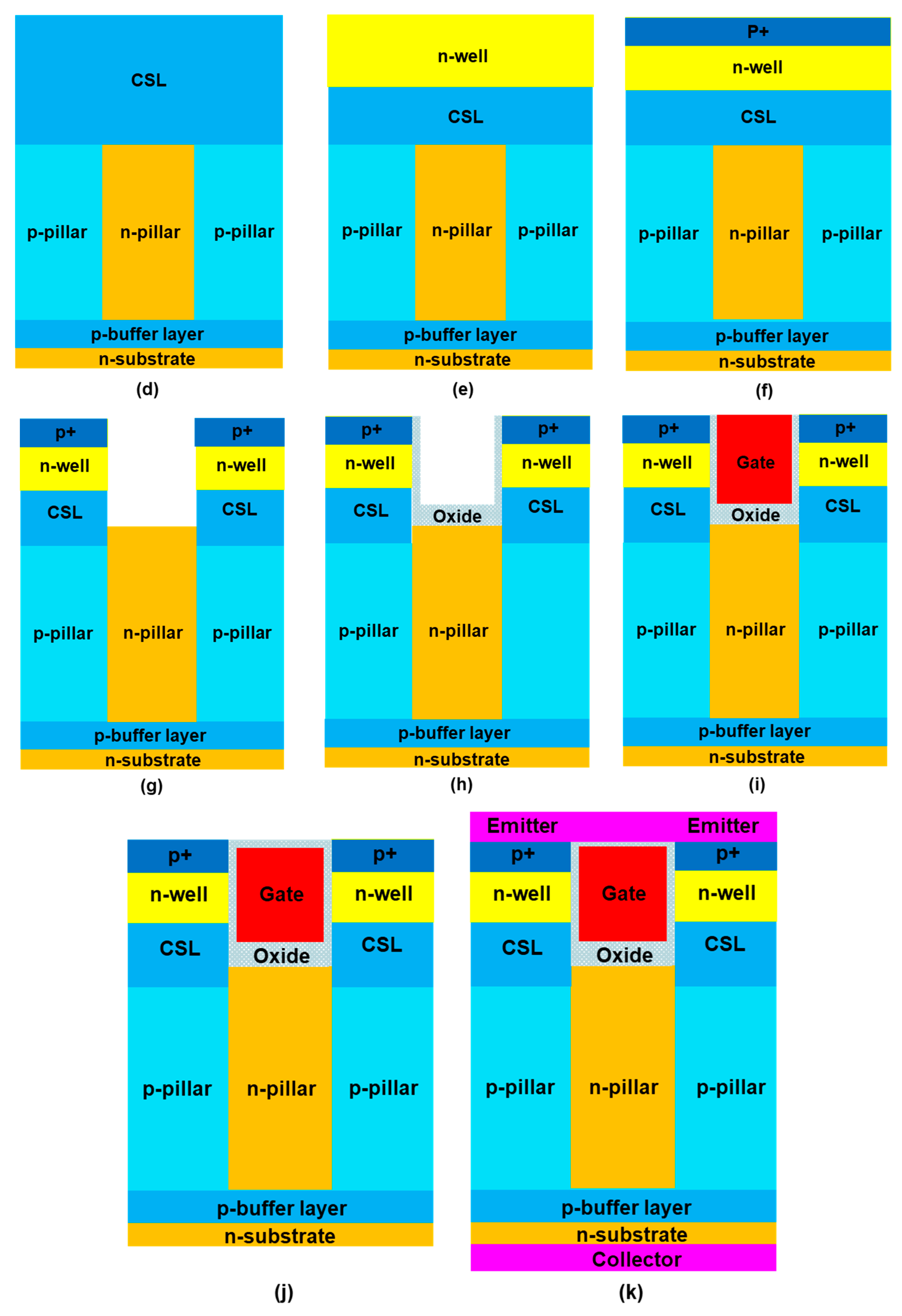
2. Device Structure
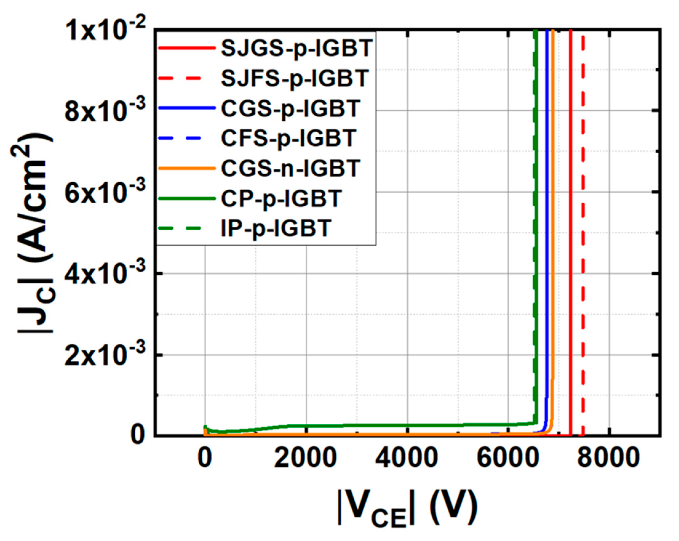
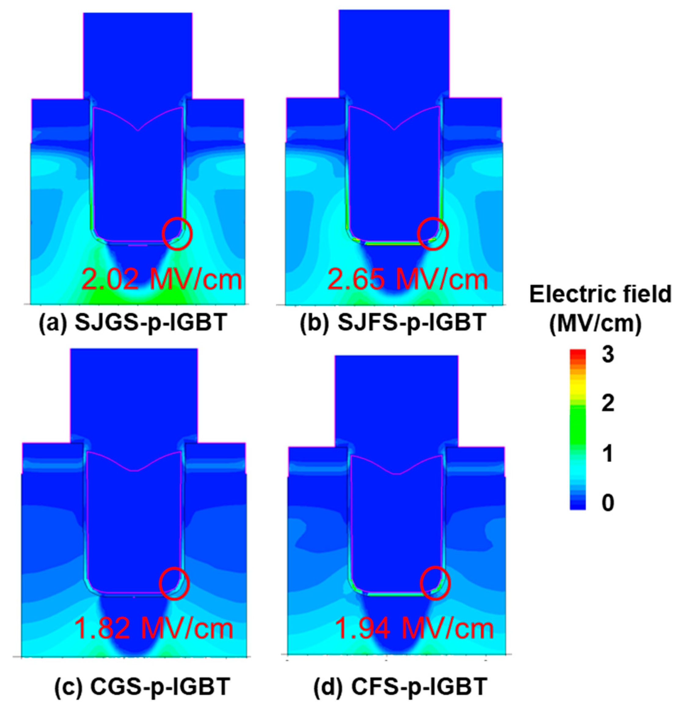
3. Static Characteristics
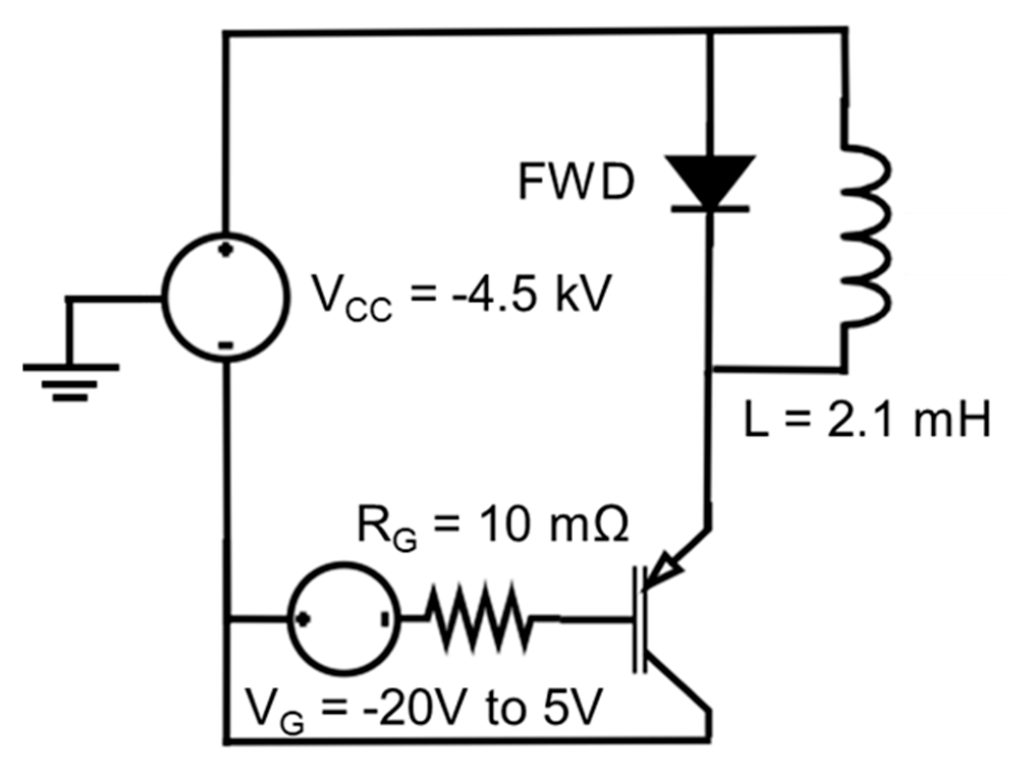
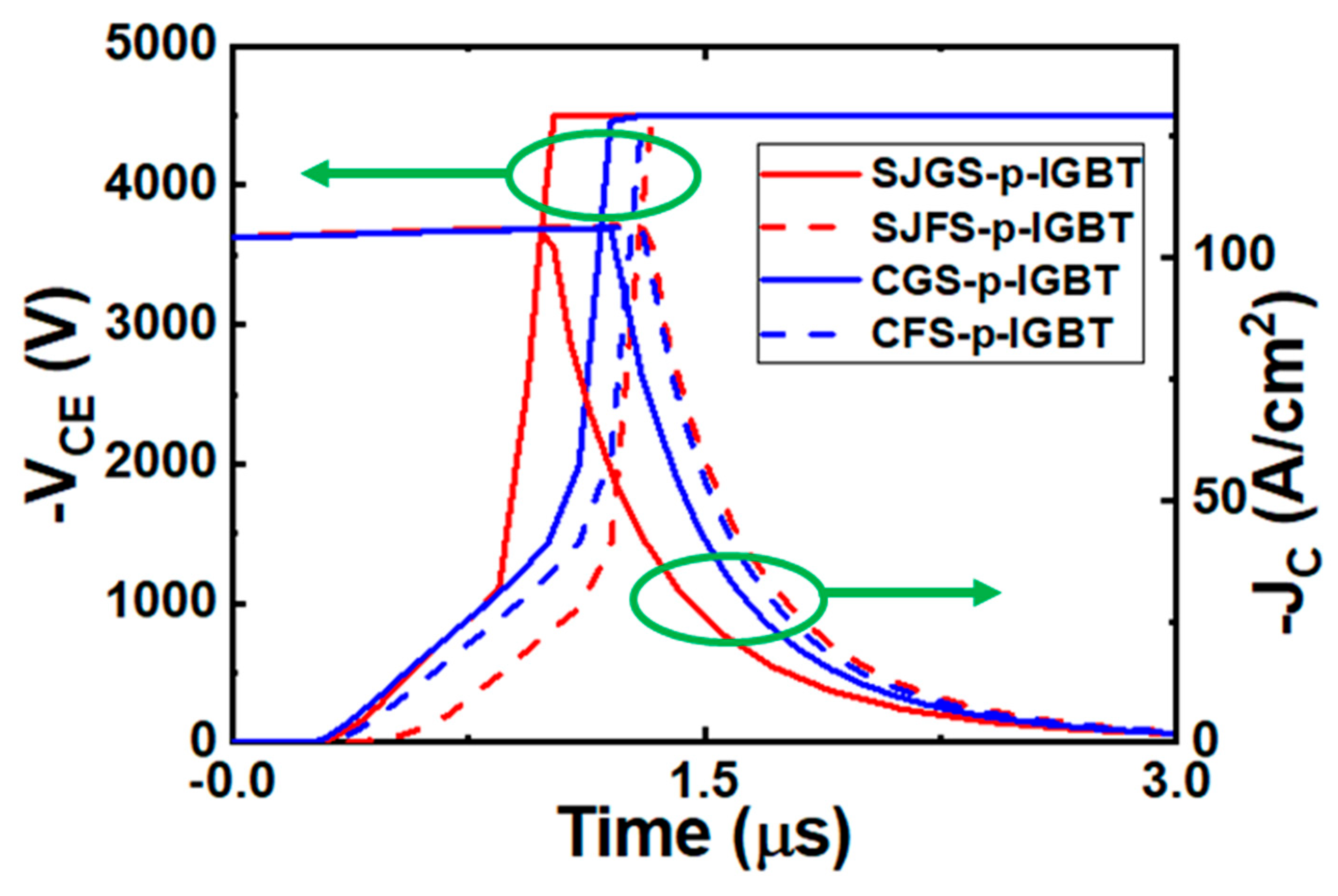
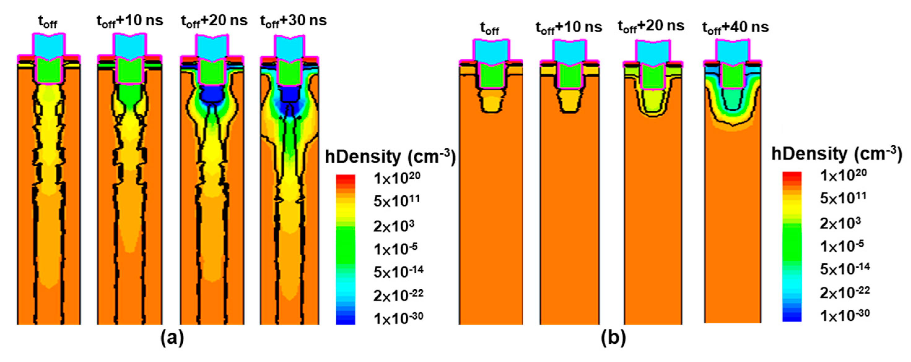
4. Dynamic Characteristics
5. Key Performance Parameters
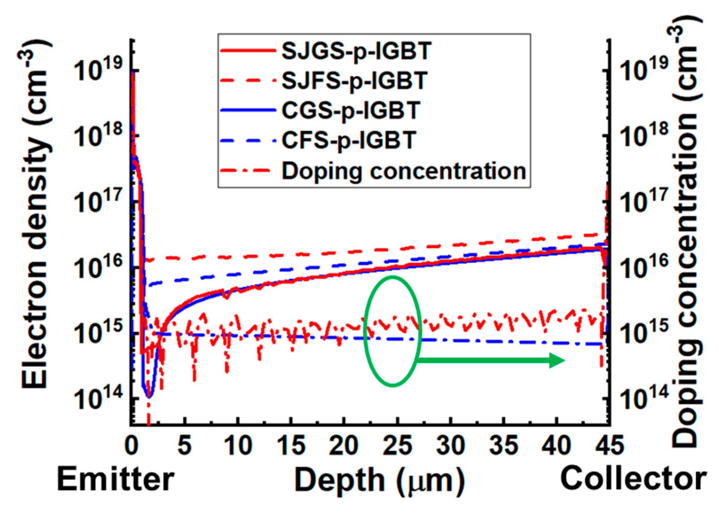
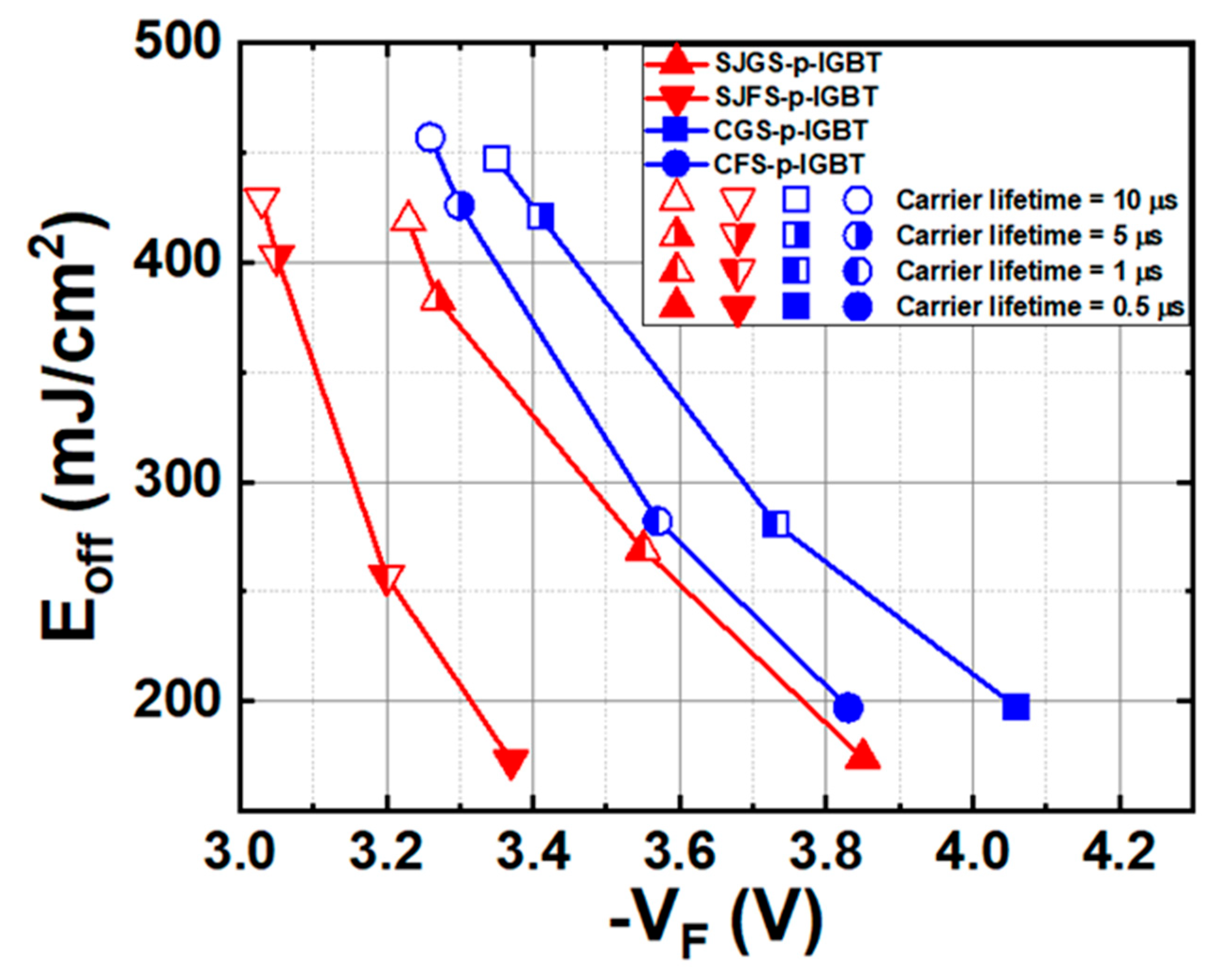
5.1. Carrier Lifetime
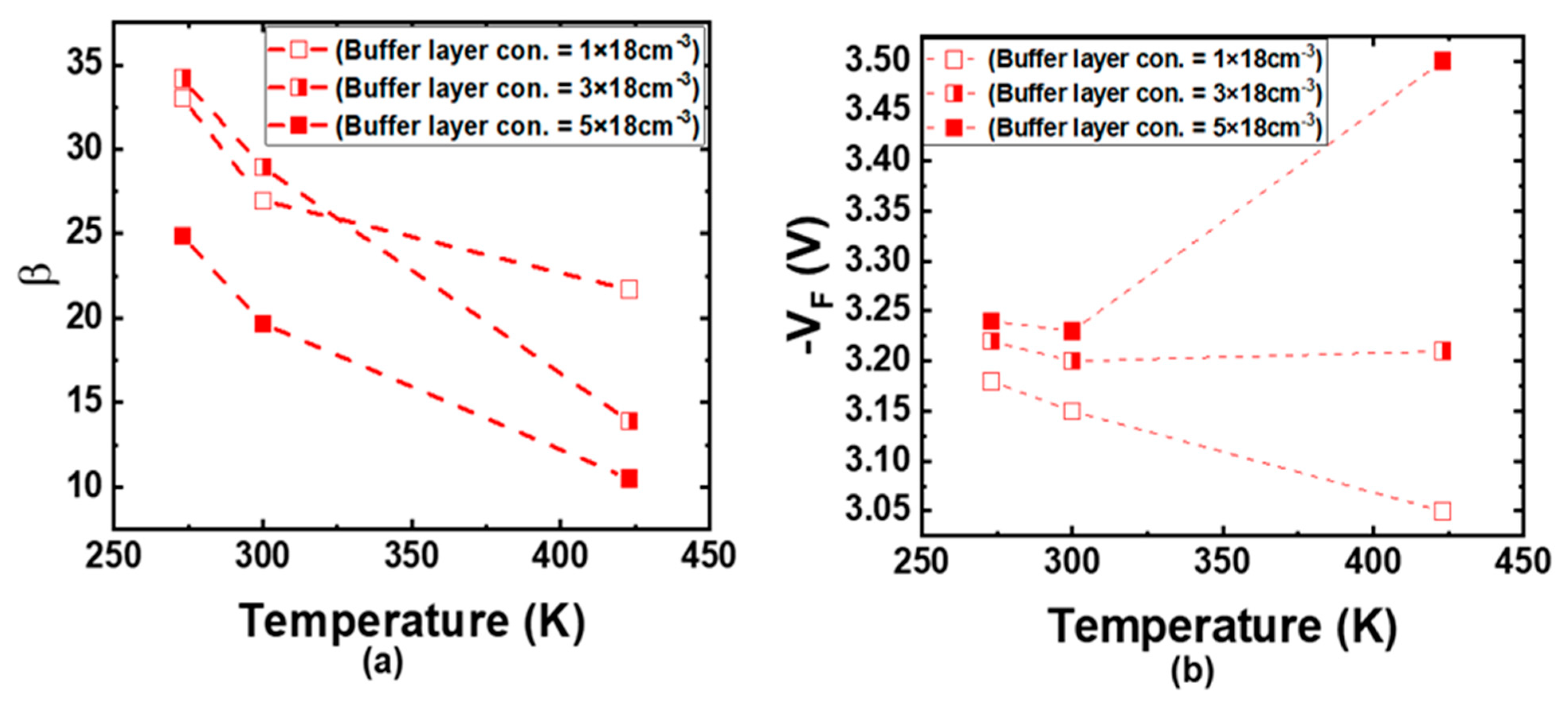
5.2. Buffer Layer Doping Concentration
5.3. Temperature Effect
6. Conclusions
Author Contributions
Funding
Data Availability Statement
Conflicts of Interest
References
- Jun, S.; In, J.; Kang, N.E.-G.; Young, M. Use of the p-floating shielding layer for improving electric field concentration of the recessed gate. In Proceedings of the 2008 IEEE International Conference on Integrated Circuit Design and Technology and Tutorial, Austin, TX, USA, 2–4 June 2008; pp. 13–16. [Google Scholar]
- Han, L.; Liang, L.; Kang, Y.; Qiu, Y. A Review of SiC IGBT: Models, Fabrications, Characteristics, and Applications. IEEE Trans. Power Electron. 2021, 36, 2080–2093. [Google Scholar] [CrossRef]
- Zhang, L.; Zheng, Z.; Lou, X. A review of WBG and Si devices hybrid applications. Chin. J. Electr. Eng. 2021, 7, 1–20. [Google Scholar] [CrossRef]
- Wang, F.; Zhang, Z. Overview of Silicon Carbide Technology: Device, Converter, System, and Application. CPSS Trans. Power Electron. Appl. 2016, 1, 13–32. [Google Scholar] [CrossRef]
- Nawaz, M.; Ilves, K. Replacing Si to SiC: Opportunities and challenges. In Proceedings of the 2016 46th European Solid-State Device Research Conference (ESSDERC), Lausanne, Switzerland, 12–15 September 2016; pp. 472–475. [Google Scholar]
- Iwamuro, N.; Laska, T. IGBT history, State-of-the-Art, and Future Prospects. IEEE Trans. Electron Devices 2017, 64, 741–752. [Google Scholar] [CrossRef]
- Sui, Y.; Wang, X.; Cooper, J.A. High-Voltage Self-Aligned p-Channel DMOS-IGBTs in 4H-SiC. IEEE Electron Device Lett. 2007, 28, 728–730. [Google Scholar] [CrossRef]
- Casady, J.B.; Pala, V.; Lichtenwalner, D.J.; Van Brunt, E.; Hull, B.; Wang, G.Y.; Richmond, J.; Allen, S.T.; Grider, D.; Palmour, J.W. New generation 10kV SiC power MOSFET and diodes for industrial applications. In Proceedings of the PCIM Europe 2015; International Exhibition and Conference for Power Electronics, Intelligent Motion, Renewable Energy and Energy Management, Nuremberg, Germany, 19–20 May 2015; pp. 96–103. [Google Scholar]
- Huang, A.Q.; Zhu, Q.; Wang, L.; Zhang, L. 15 kV SiC MOSFET: An enabling technology for medium voltage solid state transformers. CPSS Trans. Power Electron. Appl. 2017, 2, 118–130. [Google Scholar] [CrossRef]
- Zhang, Q.; Das, M.; Sumakeris, J.; Callanan, R.; Agarwal, A. 12-kV p-Channel IGBTs With Low On-Resistance in 4H-SiC. IEEE Electron Device Lett. 2008, 29, 1027–1029. [Google Scholar] [CrossRef]
- Chowdhury, S.; Chow, T.P. Performance tradeoffs for ultra-high voltage (15 kV to 25 kV) 4H-SiC n-channel and p-channel IGBTs. In Proceedings of the 2016 28th International Symposium on Power Semiconductor Devices and ICs (ISPSD), Prague, Czech Republic, 12–16 June 2016; pp. 75–78. [Google Scholar]
- Antoniou, M.; Udrea, F.; Bauer, F.E. The Superjunction Insulated Gate Bipolar Transistor Optimization and Modeling. IEEE Trans. Electron Devices 2010, 57, 594–600. [Google Scholar] [CrossRef]
- Fujihira, T. Theory of Semiconductor Superjunction Devices. Jpn. J. Appl. Phys. 1997, 36, 6254. [Google Scholar] [CrossRef]
- Li, L.; Li, Z.; Wu, Y.; Chen, P.; Rao, Q.; Yang, Y.; Yuan, Q.; Zhou, R.; Ren, M. Investigation on the carrier-storage super-junction IGBT: Characteristics, mechanism, and advantages. Microelectron. J. 2023, 142, 105993. [Google Scholar] [CrossRef]
- Antoniou, M.; Udrea, F.; Bauer, F. Optimisation of superjunction bipolar transistor for ultra-fast switching applications. In Proceedings of the 19th International Symposium on Power Semiconductor Devices and IC’s (ISPSD), Jeju, South Korea, 27–31 May 2007; pp. 101–104. [Google Scholar]
- Wu, Y.; Li, Z.; Pan, J.; Chen, C.; Yu, J.; Ren, M.; Zhang, B. 650 V Super-Junction Insulated Gate Bipolar Transistor Based on 45 μm Ultrathin Wafer Technology. IEEE Electron Device Lett. 2022, 43, 592–595. [Google Scholar] [CrossRef]
- Zhang, Q.; Jonas, C.; Ryu, S.-H.; Agarwal, A.; Palmour, J. Design and fabrications of high voltage IGBTs on 4H-SiC. In Proceedings of the 2006 IEEE International Symposium on Power Semiconductor Devices and IC’s (ISPSD), Naples, Italy, 4–8 June 2006; pp. 285–288. [Google Scholar]
- Lu, X.F.; Tian, X.; Deng, X.; Bai, Y.; Zhang, J.; Li, X.; Lu, J.; Zhu, H.; Zhong, W. Design and Optimization of Ultrahigh Voltage CSL p-channel 4H-SiC IGBT. In Proceedings of the 2019 IEEE International Conference on Electron Devices and Solid-State Circuits (EDSSC), Xi’an, China, 12–14 June 2019; pp. 1–3. [Google Scholar]
- Singh, R.; Ryu, S.-H.; Capell, D.C.; Palmour, J.W. High temperature SiC trench gate p-IGBTs. IEEE Trans. Electron Devices 2003, 50, 774–784. [Google Scholar] [CrossRef]
- Wen, Z.; Zhang, F.; Shen, Z.; Tian, L.; Yan, G.; Liu, X.; Wang, L.; Zhao, W.; Sun, G.; Zeng, Y. A Novel Silicon Carbide Accumulation Channel Injection Enhanced Gate Transistor With Buried Barrier Under Shielding Region. IEEE Electron Device Lett. 2017, 38, 941–944. [Google Scholar] [CrossRef]
- Spejo, L.B.; Knoll, L.; Minamisawa, R.A. 6.5 kV SiC PiN and JBS Diodes’ Comparison in Hybrid and Full SiC Switch Topologies. Electronics 2024, 13, 4548. [Google Scholar] [CrossRef]
- Filsecker, F.; Alvarez, R.; Bernet, S. The Investigation of a 6.5-kV, 1-kA SiC Diode Module for Medium Voltage Converters. IEEE Trans. Power Electron. 2014, 29, 2272–2280. [Google Scholar] [CrossRef]
- Mirzaee, H.; De, A.; Tripathi, A.; Bhattacharya, S. Design comparison of high power medium-voltage converters based on 6.5kV Si-IGBT/Si-PiN diode, 6.5kV Si-IGBT/SiC-JBS diode, and 10kV SiC MOSFET/SiC-JBS diode. IEEE Trans. Ind. Appl. 2014, 50, 2728–2740. [Google Scholar] [CrossRef]
- Jiang, J.-Y.; Wu, T.-L.; Zhao, F.; Huang, C.-F. Numerical Study of 4H-SiC UMOSFETs with Split-Gate and P+ Shielding. Energies 2020, 13, 1122. [Google Scholar] [CrossRef]
- Sundaramoorthy, V.; Mihaila, A.; Spejo, L.; Minamisawa, R.A.; Knoll, L. Performance Comparison of 6.5 kV SiC PiN Diode with 6.5 kV SiC JBS and Si Diodes. Mater. Sci. Forum 2022, 1062, 588–592. [Google Scholar] [CrossRef]
- Baba, M.; Tawara, T.; Morimoto, T.; Harada, S.; Kimura, H. Ultra-Low Specific on-Resistance Achieved in 3.3 kV-Class SiC Superjunction MOSFET. In Proceedings of the 2021 33rd International Symposium on Power Semiconductor Devices and ICs (ISPSD), Nagoya, Japan, 30 May 2021–3 June 2021; pp. 83–86. [Google Scholar]
- Kang, H.; Udrea, F. High Pillar Doping Concentration for SiC Superjunction IGBTs. In Proceedings of the 2018 International Semiconductor Conference (CAS), Sinaia, Romania, 10–12 October 2018; pp. 151–154. [Google Scholar]
- Kosugi, R.; Sakuma, Y.; Kojima, K.; Itoh, S.; Nagata, A.; Yatsuo, T.; Tanaka, Y.; Okumura, H. First experimental demonstration of SiC super-junction (SJ) structure by multi-epitaxial growth method. In Proceedings of the 2014 IEEE 26th International Symposium on Power Semiconductor Devices & IC’s (ISPSD), Waikoloa, HI, USA, 15–19 June 2014; pp. 346–349. [Google Scholar]
- Caughey, D.; Thomas, R. Carrier mobilities in silicon empirically related to doping and field. Proc. IEEE 1967, 55, 2192–2193. [Google Scholar] [CrossRef]
- Roschke, M.; Schwierz, F. Electron mobility models for 4H, 6H, and 3C SiC MESFETs. IEEE Trans. Electron Devices 2001, 48, 1442–1447. [Google Scholar] [CrossRef]
- Deguchi, T.; Mizushima, T.; Fujisawa, H.; Takenaka, K.; Yonezawa, Y.; Fukuda, K.; Okumura, H.; Arai, M.; Tanaka, A.; Ogata, S.; et al. Static and dynamic performance evaluation of >13 kV SiC p-channel IGBTs at high temperatures. In Proceedings of the 2014 IEEE 26th International Symposium on Power Semiconductor Devices & IC’s (ISPSD), Waikoloa, HI, USA, 15–19 June 2014; pp. 261–264. [Google Scholar]
- Tan, J.; Cooper, J.A.; Melloch, M.R. High-voltage accumulation-layer UMOSFET’s in 4H-SiC. IEEE Electron Device Lett. 1998, 19, 487–489. [Google Scholar] [CrossRef]
- Wei, J.; Zhang, M.; Jiang, H.; Li, B.; Chen, K.J. Gate structure design of SiC trench IGBTs for injection-enhancement effect. IEEE Trans. Electron Devices 2019, 66, 3034–3039. [Google Scholar] [CrossRef]
- Wei, J.; Zhang, M.; Jiang, H.; Li, B.; Zheng, Z.; Chen, K.J. Investigations of p-Shielded SiC Trench IGBT with Considerations on IE Effect, Oxide Protection and Dynamic Degradation. In Proceedings of the 2019 31st International Symposium on Power Semiconductor Devices and ICs (ISPSD), Shanghai, China, 19–23 May 2019; pp. 199–202. [Google Scholar]
- Miyake, M.; Ueno, M.; Feldmann, U.; Mattausch, H.J. Modeling of SiC IGBT turn-off behavior valid for over 5-kV circuit simulation. IEEE Trans. Electron. Devices 2013, 60, 622–629. [Google Scholar] [CrossRef]
- Hayashi, T.; Asano, K.; Suda, J.; Kimoto, T. Enhancement and control of carrier lifetimes in p-type 4H-SiC epilayers. J. Appl. Phys. 2012, 112, 64503. [Google Scholar] [CrossRef]
- Yang, X.; Li, S.; Liu, H.; Liu, A.; Zhao, Z.; Li, Y. Low Ron,sp.diff and ultra-high voltage 4H-SiC n-channel IGBTs with carrier lifetime enhancement process. In Proceedings of the 2020 17th China International Forum on Solid State Lighting & 2020 International Forum on Wide Bandgap Semiconductors China (SSLChina: IFWS), Shenzhen, China, 23–25 November 2020; pp. 42–44. [Google Scholar]
- Chu, K.-W.; Lee, W.-S.; Cheng, C.-Y.; Huang, C.-F.; Zhao, F.; Lee, L.-S.; Chen, Y.-S.; Lee, C.-Y.; Tsai, M.-J. Demonstration of lateral IGBTs in 4H-SiC. IEEE Electron Device Lett. 2013, 34, 286–288. [Google Scholar] [CrossRef]
- Kimoto, T.; Cooper, J.A. Fundamentals Silicon Carbide Technology: Growth, Characterization, Devices, Applications; Wiley: Singapore, 2014. [Google Scholar]
- Tamaki, T.; Walden, G.G.; Sui, Y.; Cooper, J.A. Numerical study of the turnoff behavior of high-voltage 4H-SiC IGBTs. IEEE Trans. Electron Devices 2008, 55, 1928–1933. [Google Scholar] [CrossRef]
- Li, X.; Luo, Y.; Fursin, L.; Zhao, J.H.; Pan, M.; Alexandrov, P.; Weiner, M. On the temperature coefficient of 4H-SiC BJT current gain. Solid-State Electron. 2003, 47, 233–239. [Google Scholar] [CrossRef]
- Luo, Y.; Fursin, L.; Zhao, J.H. Demonstration of 4H-SiC power bipolar junction transistors. Electron. Lett. 2000, 36, 1496. [Google Scholar] [CrossRef]
- Ryu, S.-H.; Agarwal, A.K.; Singh, R.; Palmour, J.W. 1800 V NPN bipolar junction transistors in 4H-SiC. IEEE Electron Device Lett. 2001, 22, 124–126. [Google Scholar]
- Tang, Y.; Fedsion, J.B.; Chow, T.P. An implanted-emitter 4H-SiC bipolar transistor with high current gain. In Proceedings of the 58th DRC. Device Research Conference, Denver, CO, USA, 19–21 June 2000; pp. 131–132. [Google Scholar]
- Adachi, K.; Johnson, C.M.; Ortolland, S.; Wright, N.G.; O’Neill, A.G. TCAD Evaluation of Double Implanted 4H-SiC Power Bipolar Transistors. Mater. Sci. Forum 2000, 338, 1419–1422. [Google Scholar] [CrossRef]


| Parameters | Conventional Planar Gate p-IGBT | Improved Planar Gate p-IGBT | Conventional Trench Gate n-IGBT | Conventional Trench Gate p-IGBT | Superjunction Trench Gate p-IGBT |
|---|---|---|---|---|---|
| Buffer layer depth (μm) | 2.5 | 2.5 | 2.5 | 2.5 | 2.5 |
| Buffer layer doping (cm−3) | 1 × 10¹⁸ | 1 × 10¹⁸ | 1 × 10¹⁸ | 1 × 10¹⁸ | 1 × 10¹⁸ |
| Drift region depth (μm) | 45 | 45 | 45 | 45 | 45 |
| Drift region doping (cm−3) | 1 × 10¹⁵ | 1 × 10¹⁵ | 1 × 10¹⁵ | 1 × 10¹⁵ | 1 × 10¹⁵ |
| CSL doping (cm−3) | 1 × 10¹⁶ | 1 × 10¹⁶ | 1 × 10¹⁶ | 1 × 10¹⁶ | 1 × 10¹⁶ |
| Channel length (μm) | 1.5 | 0.5 | 0.5 | 0.5 | 0.5 |
| JFET width (μm) | 3 | 2.2 | -- | -- | -- |
| Cell pith (μm) | 15 | 4.4 | 2.2 | 2.2 | 2.2 |
Disclaimer/Publisher’s Note: The statements, opinions and data contained in all publications are solely those of the individual author(s) and contributor(s) and not of MDPI and/or the editor(s). MDPI and/or the editor(s) disclaim responsibility for any injury to people or property resulting from any ideas, methods, instructions or products referred to in the content. |
© 2025 by the authors. Licensee MDPI, Basel, Switzerland. This article is an open access article distributed under the terms and conditions of the Creative Commons Attribution (CC BY) license (https://creativecommons.org/licenses/by/4.0/).
Share and Cite
Kang, K.-M.; Hu, J.-W.; Huang, C.-F. Simulation Study on 6.5 kV SiC Trench Gate p-Channel Superjunction Insulated Gate Bipolar Transistor. Micromachines 2025, 16, 758. https://doi.org/10.3390/mi16070758
Kang K-M, Hu J-W, Huang C-F. Simulation Study on 6.5 kV SiC Trench Gate p-Channel Superjunction Insulated Gate Bipolar Transistor. Micromachines. 2025; 16(7):758. https://doi.org/10.3390/mi16070758
Chicago/Turabian StyleKang, Kuan-Min, Jia-Wei Hu, and Chih-Fang Huang. 2025. "Simulation Study on 6.5 kV SiC Trench Gate p-Channel Superjunction Insulated Gate Bipolar Transistor" Micromachines 16, no. 7: 758. https://doi.org/10.3390/mi16070758
APA StyleKang, K.-M., Hu, J.-W., & Huang, C.-F. (2025). Simulation Study on 6.5 kV SiC Trench Gate p-Channel Superjunction Insulated Gate Bipolar Transistor. Micromachines, 16(7), 758. https://doi.org/10.3390/mi16070758